

Page 1
\
CDB5461AU
CDB5461AU Evaluation Board & Software
Features
z Voltage and Current Interface
z USB communication with PC
z On-board C8051F320 microcontroller
z On-board Voltage Reference
z Lab Windows
– Register Setup & Chip Control
– FFT Analysis
– Time Domain Analysis
– Noise Histogram Analysis
z "Auto-boot" Demo with serial EEPROM
– Collected by On-board Microcontroller
– Available on External Header
®
/ CVI™ Evaluation Software
General Description
The CDB5461AU is an inexpensive tool designed to
evaluate the functionality and performance of the
CS5461A. The evaluation board includes an LT1019
voltage reference, a C8051F320 microcontroller with
a USB interface, and firmware. The microcontroller
controls the serial communication between the evaluation board and the PC via the firmware, enabling
quick and easy access to all of the CS5461A's registers and functions.
The CDB5461A includes software for Data Capture,
Time Domain Analysis, Histogram Analysis, and Frequency Domain Analysis.
ORDERING INFORMATION
CDB5461AU Evaluation Board
REF
VIN+
VIN-
IIN+
IIN-
+2.5V
reference
+5V GND
IN OUT
VREF
CS5461A
4.096MHz
Crysta l
VD+_EXT
CS
SDI
SDO
SCLK
INT
RESET
E1
E2
E3
MODE
Vu+_EXT
SERIAL
EERPOM
C8051F320
Reset
Circuirty
RESET
BUTTON
USB
http://www.cirrus.com
Copyright © Cirrus Logic, Inc. 2006
(All Rights Reserved)
DEC ‘06
DS661DB1
Page 2

CDB5461AU
TABLE OF CONTENTS
– TABLE OF CONTENTS ............................................................... ... ... ... ... .... .............................. 2
– LIST OF FIGURES ..................................................................................................................... 3
– LIST OF TABLES ...................................................................................................................... 3
1. HARDWARE .............................................................................................................................4
1.1 Introduction ............................ .... ... .......................................... ... ... ..................................... 4
1.2 Evaluation Board Overview ..................................................................... ... ... .... ... ... ...........4
1.2.1 Analog Section ....................................... .... ... ... ... .......................................... ... .... . 5
1.2.2 Digital Section ........ .......................................... .......................................... ...........6
1.2.3 Power Supply Section ......................................... .... ... ... ... ... .... ... ... ........................7
1.3 Auto-boot Mode .. ... ... .... ... ... ... .......................................... .... ... ... ... ... .................................. 8
2. SOFTWARE .............................................................................................................................. 9
2.1 Installation Procedure ............................ .... ... ... ... .... ... ... .......................................... ... ... ..... 9
2.2 Using the Software ................................. .... ... .......................................... ... ........................ 9
2.3 Start-Up Window .... ... .......................................... .... ... ... ... .... .............................................. 9
2.3.1 Setup ............................. ... ... .......................................... ...................................... 10
2.3.2 Quit ...................... .......................................... .......................................... ............11
2.3.3 Menu ................ ... .......................................... .......................................... ............12
2.4 Setup Window .. ... ... .......................................... ... .... ... .......................................... ... ... ...... 12
2.4.1 Refresh Screen Button ........................................................................................ 13
2.4.2 Reset DUT Button ...................................... .......................................... ...............13
2.4.3 CS5461A Crystal Frequency ............................................................................... 13
2.4.4 Configuration Register Panel .............................................................................. 14
2.4.5 Mask Register/Status Register Panel .................................................................14
2.4.6 Cycle Count / PulseRateE / PulseWidth / VSAGlevel / VSAGduration Registers 14
2.4.7 Control Register ............... ... ... ... .... .......................................... ... ... ... .... ... ............14
2.5 Calibration Window ............. .......................................... ... .... ... ... ... ... ................................ 15
2.5.1 Offset & Gain Registers ................................................................ ... .... ... ... ... ......15
2.5.2 Performing Calibrations ................. ... ... ... .... ... ... ... .... ......................................... ... 15
2.6 Conversion Window ......... ... ... .... ... ... ... ... .......................................................................... 17
2.6.1 Single Conversion Button .................................................................................... 17
2.6.2 Continuous Conversion Button ............................................................... ... ... ... ... 17
2.6.3 Standby & Sleep Mode Buttons ............. .... ... ... ... .... ... ... ... ................................... 17
2.6.4 Power Up Button .................................................................................................18
2.6.5 Temperature Settings Window ......................... ... .... ... ... ... ... .... ... .........................18
2.6.6 Write Data to File Window ................ ... ... .... ... ... .......................................... ... ... ... 18
2.7 Pulse Rate Window ................................ .... .......................................... ... ... ......................18
2.7.1 Integration Seconds Field ................................................................................... 18
2.7.2 Periods to Average Field .................................. ... .... ... ... ... ... .... ... ... ... .... ...............18
2.7.3 Start Button ............ ... .......................................... .......................................... ......19
2.8 Data Collection Window ................................................................................................... 19
2.8.1 Time Domain / FFT / Histogram Pull-down ......................................................... 19
2.8.2 Config Button ......................... ... .... ... ... ... .... ... .......................................... ... .........19
2.8.3 Collect Button ................................ ... ... ... .... ... ... .......................................... ... ... ... 20
2.8.4 Output Button ... ... ... .......................................... ... .... ... ... ... ................................... 20
2.8.5 Zoom Button .................. .......................................... ......................................... ... 20
2.8.6 Channel Select Button ........................................................................................ 20
2.8.7 Config Window .................................... ... .... .......................................... ...............20
2.8.8 Collecting Data Sets ............................................................................................21
2.8.9 Retrieving Saved Data from a File ...................................................................... 21
2.8.10 Analyzing Data ..................................................................................................21
2.8.11 Histogram Information ....................................................................................... 22
2.8.12 Frequency Domain Information ................... ............................................. .........24
2 DS661DB1
Page 3

CDB5461AU
2.8.13 Time Domain Information ......................... ...... ....... ...... ...... ....... ...... ....... ...... ...... 25
2.9 EEPROM Window ..................................................................................... ...................... 26
2.9.1 Read EEPROM ................................................................................................... 26
2.9.2 Write EEPROM ................................................................................................... 26
2.9.3 Debug Window .......................... .... ... .......................................... ... ... ................... 26
3. SCHEMATICS ....................................................................................................................... 28
4. LAYOUT ............................................................................................................................... 32
LIST OF FIGURES
Figure 1. CDB5461AU Assembly Drawing...................................................................................... 4
Figure 2. CDB5461AU Start-up Window......................................................................................... 9
Figure 3. Establishing a USB Connection..... ... ... .......................................................................... 10
Figure 4. USB Error Message....................................................................................................... 10
Figure 5. Selecting a Data File for Further Analysis.......................... ... ... ... ... .... ... ... ... ................... 11
Figure 6. Quit Window................................................................................................................... 11
Figure 7. Menu Pull-down Options................................................................................................ 12
Figure 8. Setup Window................................................................................................................ 13
Figure 9. Calibration Window........................................................................................................ 15
Figure 10. Conversion Window..................... ... .......................................... ... .... ............................ 17
Figure 11. Pulse Rate Output Window.......................................................................................... 18
Figure 12. Data Collection Window...............................................................................................19
Figure 13. Histogram Analysis...................................................................................................... 22
Figure 14. FFT Analysis................................................................................................................ 24
Figure 15. Time Domain Analysis................................................................................................25
Figure 16. EEPROM Window........................................................................................................ 26
Figure 17. Debug Window............................................................................................................. 27
Figure 18. Analog Inputs............................................................................................................... 28
Figure 19. CS546x and Socket..................................................................................................... 29
Figure 20. Microcontroller and USB Interface............................................................................... 30
Figure 21. Power Supplies............................................................................................................ 31
Figure 22. Top Silk Screen............................................................................................................ 32
Figure 23. Topside Layer.............................................................................................................. 33
Figure 24. Bottomside Layer......................................................................................................... 34
Figure 25. Bottom Silk Screen ...................................................................................................... 35
LIST OF TABLES
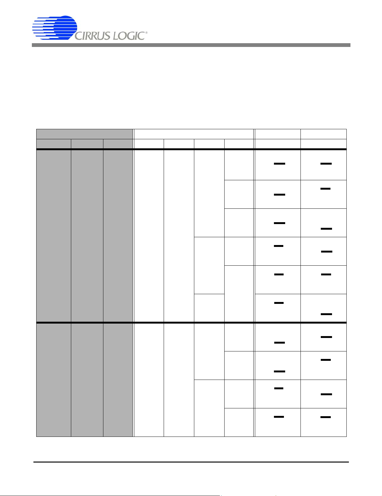
Table 1. Internal Voltage Reference Selection for VREF................................................................ 5
Table 2. External Voltage Reference Selection for VREF............................................................... 5
Table 3. Voltage and Current Channel Input Signal Selection........................................................ 6
Table 4. Power Supply Connections...............................................................................................7
DS661DB1 3
Page 4
CDB5461AU
1. HARDWARE
1.1 Introduction
The CDB5461AU evaluation board provides a quick means of evaluating the CS5461A Power Meter IC. The
CDB5461AU evaluation board operates from a single +5 V power supply. The evaluation board interfaces the
CS5461A to a PC via an USB interface. To accomplish this, the board comes equipped with a C8051F320 microcontroller and a USB interface. Additionally, CDB5461AU GUI software provides easy access to the internal
registers of the CS5461A, and provides a means to display the performance in the time domain or frequency domain.
1.2 Evaluation Board Overview
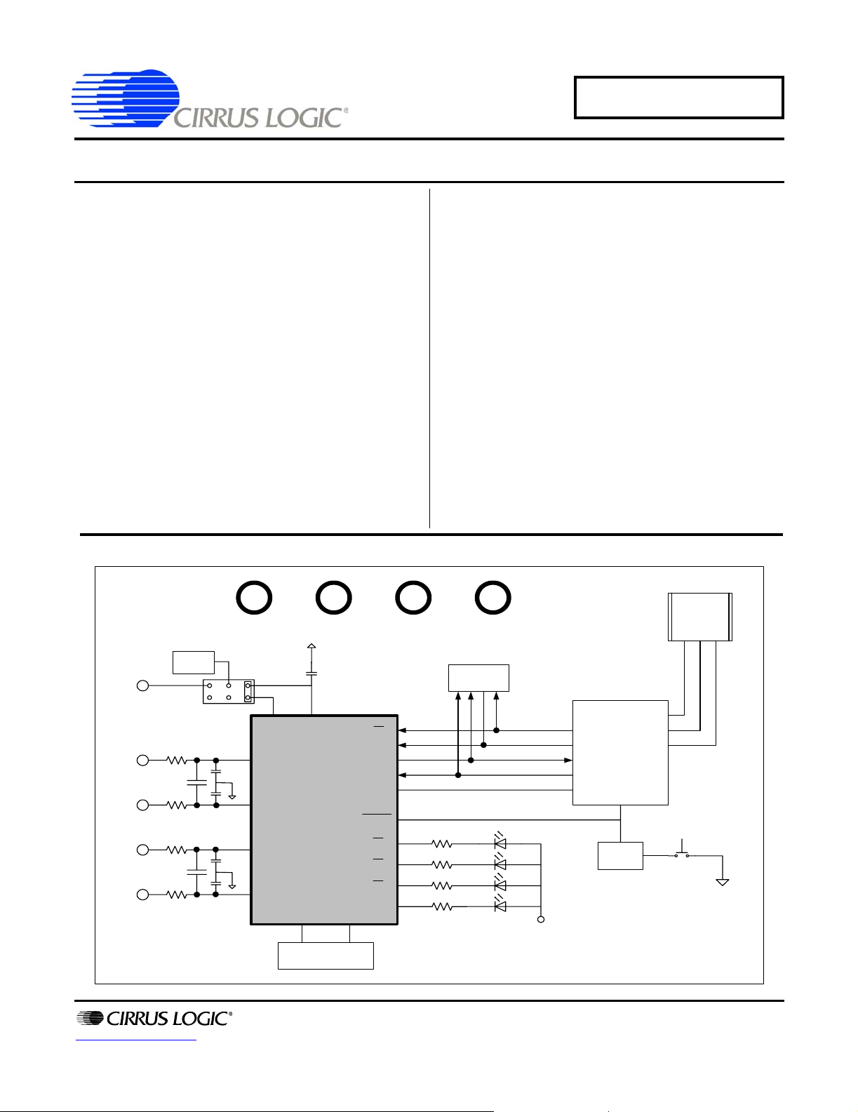
The board is partitioned into two main sections: analog and digital. The analo g section consists of the CS5461A and
a precision voltage reference. The digital section consists of the C8051F320 microcontroller, EEPROM, the hardware test switches, the reset circuitry, and the USB interface. The board also has a user friendly power supply connection.
REF+
GND
GND
VIN+
VIN-
GND
GND
IIN+
IIN-
GND
J14
J23
J27
JP3
GND
TP23
TP22
TP21
TP25
TP20
JTAG
TP24
S1
RESET
U3
TP26
U9
U11
J10
J13
J15
J16
JP5
GND
J1
U1
8051
LED_EN
1
LED_EN
1
LED_EN
1
LED_EN
1
USB
TP27
J18
AUTO-BOOT
J2
1
ENABLE
U10
U8
D1
EVENT
ERROR
TP1
E1
E2
E3
MODE
U5
JP4
GND
RESET
U2
INT
MODE
EECS
SCLK
MISO
MOSI
J40
1
E1
E2
E3
CS
21 22
2
Vu+_EXTVD+_EXTGND+5V
8051_REGIN
+5V
VD+
J9
TP30
PFMON
J6
JP2
GND
J5J4J3
JP1
GND
GND
VD+
U4
TP2
LT1019
JP6
GND
REF+
GND
VREF
VIN+
VIN-
VREF
GND
GND
VREF
IIN+
IIN-
VREF
GND
J12
J17
J26
J22
J24
VIN+
VIN-
IIN+
IIN-
TP9
TP11
TP12
TP13
CDB5460A_61A_63
CDB5461AU REV X
XU6
CPUCLK
TP10
VREF
VA+
GND VD+GND
VD+
VD+_EXT
+5V
+3.3V
J8
XOUT XIN
TP7 TP8
4.096MHz
U6
5461A
J25
VREFIN
VREFOUT
Vu+_EXT
Y1
Figure 1. CDB5461AU Assembly Drawing
4 DS661DB1
Page 5
CDB5461AU
1.2.1 Analog Section
The CDB5461AU evaluation board provides screw-type terminals (J23, J27 ) to connect in put signals to the voltage
and current channels. The screw terminals are labels as VIN+, VIN1, IIN+, and IIN-. A simple R-C network at each
channel input provides a simple anti-alias filter.
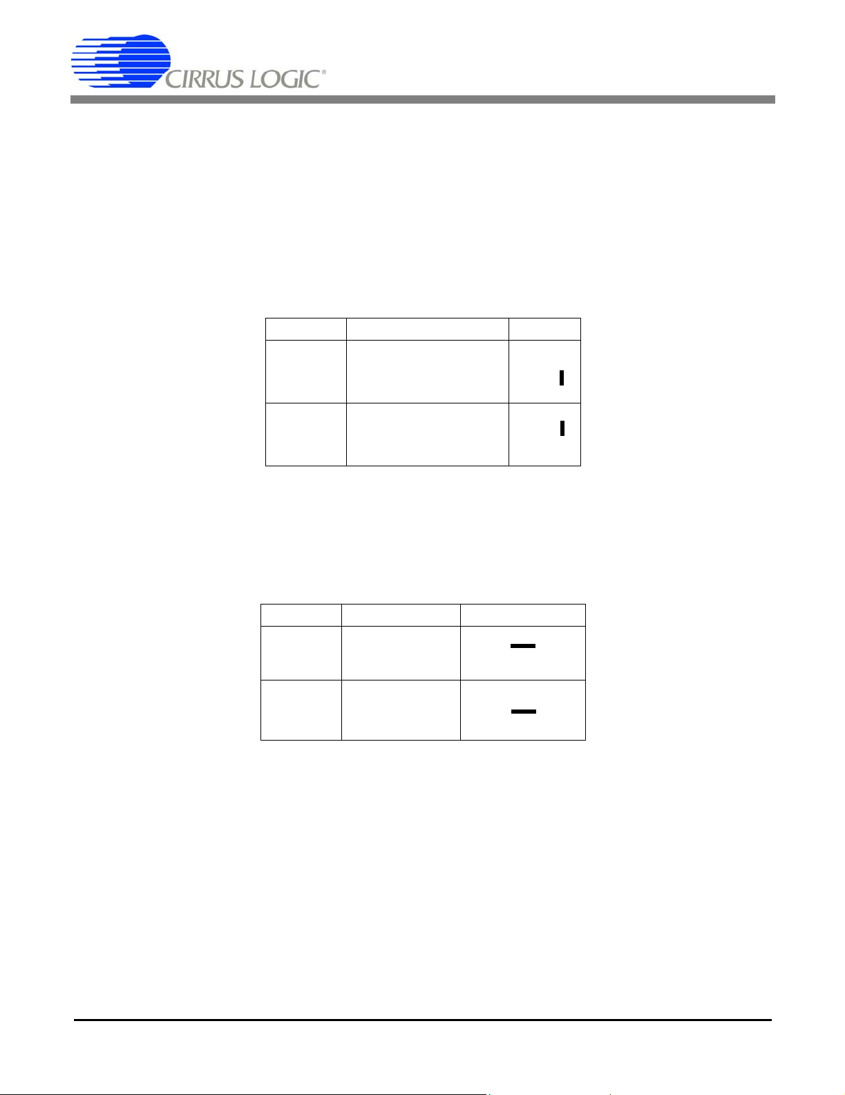
The evaluation board provides three voltage reference options for VREFIN to the CS5461A. The three voltage reference options include: VREFOUT from CS5461A, the on-board +2.5V reference, and external REF+ (screw terminal J14). Table 1 and Table 2 illustrate the options available for VREFIN. With a jumper on J25 in the position labeled
VREFOUT, the reference is supplied by the on-chip voltage reference. With a jumper on J25 in th e posi tion labele d
VREF, the reference is supplied by an off-chip voltage reference.
Reference Description J25
VREF
VREFOUT
VREF
Selects on-Chip
Reference (25ppm/
Selects External or
LT1019 Reference(J12)
°C)
VREFIN
VREFOUT
(Default)
VREFIN
VREFOUT
Table 1. Internal Voltage Reference Selection for VREF
VREF
O
O
O
O
Table 2 illustrates the options available for VREF. With a jumper on J12 in position LT1019, the LT1019 provides a
+2.5V reference (the LT1019 was chosen for its low drift - typically 5 ppm/°C). By setting the jumper on J12 to position
REF+, an external voltage reference is supplied via screw terminal J14's REF+ input.
Reference Description J12
LT1019
REF+
Selects on-Board
LT1019 Reference
(5ppm/
°C)
Selects External
Reference Source
(J6)
LT1019
REF+
LT1019
REF+
O VREF
O O VREF
O VREF
O O VREF
(Default)
Table 2. External Voltage Reference Selection for VREF
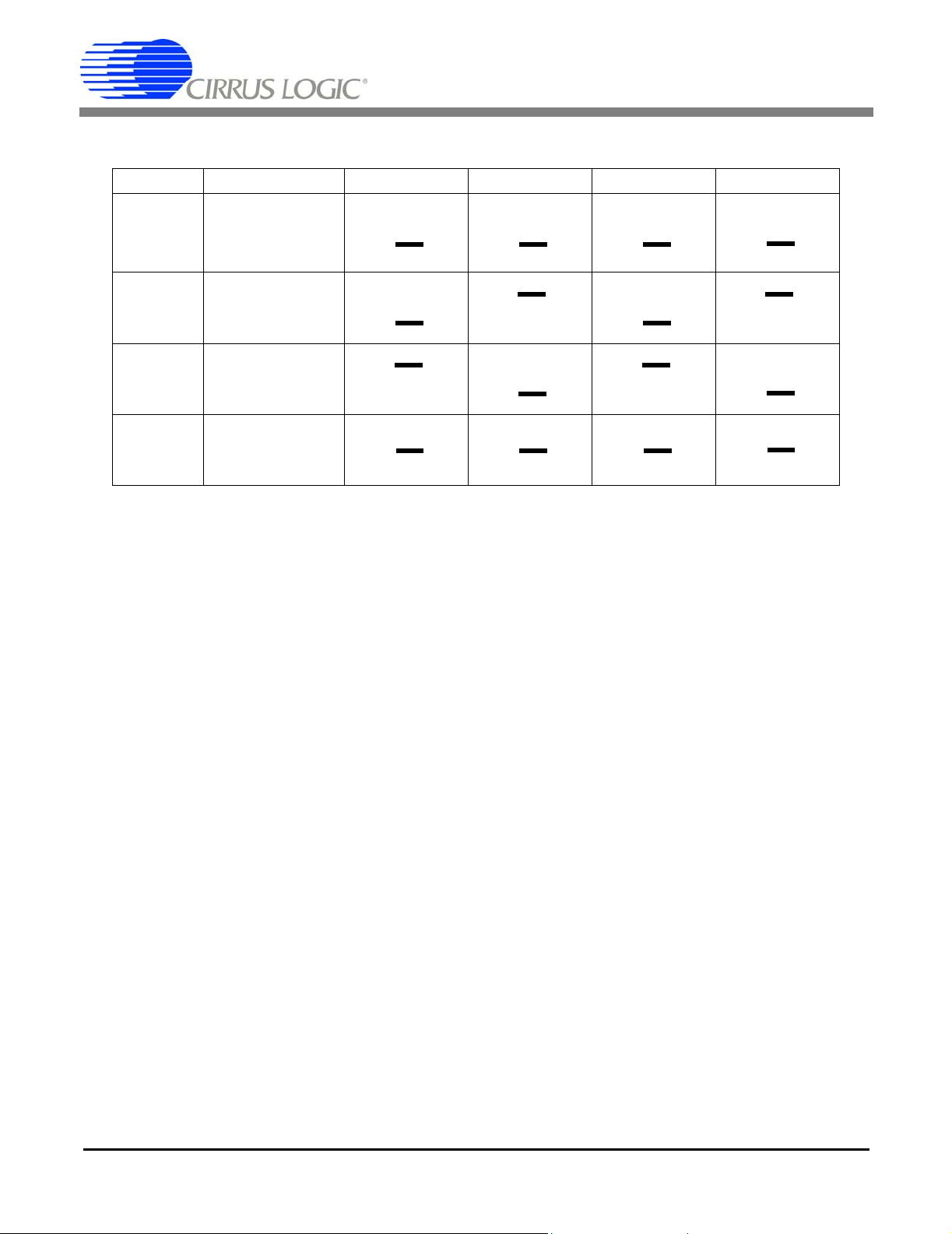
The three input signal options for the voltage (VIN±) and current (IIN±) channel input include: an external signal
(screw terminals J23 and J27), GND or VREF. Table 3 illustrates the options available. By installing jumpers on J17
to position VIN+, J22 to position VIN-, J24 to position IIN+ and J26 to position IIN-, the input voltage signal is supplied
from the screw terminals J23 and J27. With a jumper on J17, J22, J24 and J26 in the GND position, the inputs are
connected to analog ground (AGND). With a jumper on J17, J22, J24 and J26 in position
VREF, the inputs are con-
nected to the reference voltage selected on J12.
DS661DB1 5
Page 6
CDB5461AU
INPUT Description J17 J22 J24 J26
VIN± or IIN±
VIN± or IIN±
GND
VREFIN
Selects External
Signal
Selects External
Signal
Selects Grounding
the Input
Selects Reference
Source
GND
VREF
VIN+
GND
VREF
VIN+
GND
VREF
VIN+
GND
VREF
VIN+
O VIN+
O O VIN+
O O VIN+
(Default)
O VIN+
O O VIN+
O O VIN+
O VIN+
O O VIN+
O O VIN+
O VIN+
O O VIN+
O O VIN+
VIN-
VREF
GND
VIN-
VREF
GND
VIN-
VREF
GND
VIN-
VREF
GND
O VIN-
O O VIN-
O O VIN-
(Default)
O VIN-
O O VIN-
O O VIN-
O VIN-
O O VIN-
O O VIN-
O VIN-
O O VIN-
O O VIN-
GND
VREF
IIN+
GND
VREF
IIN+
GND
VREF
IIN+
GND
VREF
IIN+
O IIN+
O O IIN+
O O IIN+
(Default)
O IIN+
O O IIN+
O O IIN+
O IIN+
O O IIN+
O O IIN+
O IIN+
O O IIN+
O O IIN+
IIN-
VREF
GND
IIN-
VREF
GND
IIN-
VREF
GND
IIN-
VREF
GND
O IIN-
O O IIN-
O O IIN-
(Default)
O IIN-
O O IIN-
O O IIN-
O IIN-
O O IIN-
O O IIN-
O IIN-
O O IIN-
O O IIN-
Table 3. Voltage and Current Channel Input Signal Selection
1.2.2 Digital Section
The digital section contains the microcontroller, USB interface, JTAG header, reset circuitry, and an external interface header (J40). The microcontroller interfaces the SPI of CS5461A with the USB connection to the PC, enabling
GUI software to access all the CS5461A registers and functions. Interface header, J40, is provided to allow the
CDB5461AU to be connected to an external energy registration device or an external microcontroller. To connect
the CS5461A to an external microcontroller, R59, R60, R61, and R62 must be removed from the board. The ene rgy
output pins E1, E2, and E3 are routed to LEDs which provide a simple visual check of the energy output pulses. The
Mode pin is also routed to an LED to indicate whether the CS5461A is in auto-boot mode. Jumpers J10, J13, J15,
and J16 are equipped at the factory with jumpers to enable the LEDs.
6 DS661DB1
Page 7
CDB5461AU
1.2.3 Power Supply Section
Table 4 illustrates the power supply connections to the evaluation board. The +5 binding post (J3) supplies the positive analog (VA+) for the CS5461A and the +2.5V reference. The VD+_EXT binding post (J5) supplies the digital
section of the CS5461A (VD+) and level shifters. Jumper J8 allows the VD+ supply to be sourced from the VD+_EXT
binding post (J5), the +5V binding post (J3), or the regulated 3.3V supply derived from the microcontroller. The
Vu+_EXT (J6) binding post supplies the positive supp ly for the 8051 microcontroller (8051_REGIN). Jumper J9 allows the 8051_REGIN supply to be so urced from either the Vu+_EXT binding post (J6), +5V binding post (J3) or
VD+_EXT binding post (J5).
Power Supplies Power Post Connections VD+ 8051-REGIN
Analog (VA+) Digital (VD +) 8051 (Vu+)
+5V GND VD+EXT VU+EXT J8 J9
+5 +5 +5 +5 0
+5 +3.3 +5 +5 0
Table 4. Power Supply Connections
NC
+5
NC
NC
+3.3
NC
+5
NC
NC
+5
NC
+5
NC
+5
VD+_EXT
+5
+3.3
VD+_EXT
+5
+3.3
VD+_EXT
+5
+3.3
VD+_EXT
+5
+3.3
VD+_EXT
+5
+3.3
VD+_EXT
+5
+3.3
VD+_EXT
+5
+3.3
VD+_EXT
+5
+3.3
VD+_EXT
+5
+3.3
VD+_EXT
+5
+3.3
O VD+
O O VD+
O O VD+
(Default)
O VD+
O O VD+
O O VD+
O VD+
O O VD+
O O VD+
O VD+
O O VD+
O O VD+
O VD+
O O VD+
O O VD+
O VD+
O O VD+
O O VD+
O VD+
O O VD+
O O VD+
O VD+
O O VD+
O O VD+
O VD+
O O VD+
O O VD+
O VD+
O O VD+
O O VD+
Vu+_EXT
+5
VD+
Vu+_EXT
+5
VD+
Vu+_EXT
+5
VD+
Vu+_EXT
+5
VD+
Vu+_EXT
+5
VD+
Vu+_EXT
+5
VD+
Vu+_EXT
+5
VD+
Vu+_EXT
+5
VD+
Vu+_EXT
+5
VD+
Vu+_EXT
+5
VD+
O 8051
O O 8051
O O 8051
(Default)
O 8051
O O 8051
O O 8051
O 8051
O O 8051
O O 8051
O 8051
O O 8051
O O 8051
O 8051
O O 8051
O O 8051
O 8051
O O 8051
O O 8051
O 8051
O O 8051
O O 8051
O 8051
O O 8051
O O 8051
O 8051
O O 8051
O O 8051
O 8051
O O 8051
O O 8051
DS661DB1 7
Page 8

CDB5461AU
1.3 Auto-boot Mode
With a jumper connection on J18 (AUTO-BOOT ENABLE), the CS5461A operates in auto-boot mode and the
CDB5461AU board operates in a stand-alone manner without connecting to a PC. When in auto-boot mode, a hardware reset (pressing on S1) will cause the CS5461A to boot up using the serial data from the serial EEPROM on
the board (U10). When the CS5461A is in auto-boot mode, the SPI connections between the microcontroller and
the CS5461A are removed and GUI software can not access the CS5461A registers and functions.
The EEPROM must be programmed prior to the auto-boot sequence. When the CDB5461AU Evaluation Board is
sent from the factory, the EEPROM is programmed with the following CS5461A command/data sequence:
– 40 00 00 61
– Set configuration Register, turn high-pass filters on, set K = 1;
– 4C 00 7D 00
– Set PulseRateE1,2 Register to 1000 Hz;
– 74 00 00 04
– Unmask bit #2 (LSD) in the Mask Register
–E8
– Start continuous conversion
– 78 00 01 00
– Write to the STOP bit in the Control Register, to terminate auto-boot sequence.
This sequence programs the CS5461A for continuous conversion mode. If voltage and current signals are applied
to the inputs, the CS5461A will issue pulses on the /E1, /E2 and /E3 pins. See the CS5460A data sheet for more
details on auto-boot.
8 DS661DB1
Page 9
CDB5461AU
2. SOFTWARE
The evaluation board comes with software and an USB cable to link the evaluation board to the PC. The eva luation
software was developed with Lab Windows
The evaluation software is available for download on the Cirrus Logic web site at http://www.cirrus.com/industrial-
software and was designed to run under Windows 2000™ or Windows XP®.
2.1 Installation Procedure
To install the software, go to the Cirrus Logic web si te at http://www.cirrus.com/industrialsoftware and refer to application note AN278.
2.2 Using the Software
Before launching the software, check all jumper settings on the CDB54 61AU evaluation bo ard as descr ibe d in se ction 1, and connect the board to an open USB port on the PC using the provided cable. Once the board is powe red
on, the software program can be launched.
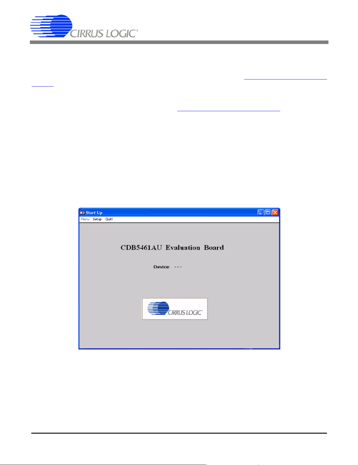
2.3 Start-Up Window
When the software is launched, the Start-Up window will appear. This window contains information concerning the
software’s title, revision number, copyright date, etc. See Figure 2.
®
/CVI™, a software development package from national Instruments.
Figure 2. CDB5461AU Start-up Window
At the top of the screen is a menu bar which displays user options. The menu bar has three items: Menu, Setup, and
Quit. Initially Menu is disabled. After establishing a link to a data source the Menu item will become available.
DS661DB1 9
Page 10
CDB5461AU
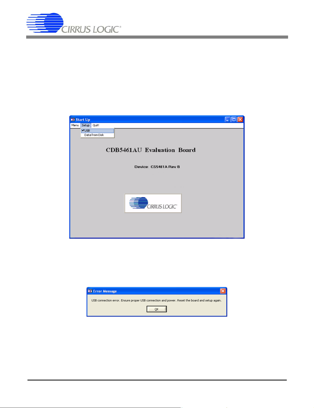
2.3.1 Setup
Setup allows user to establish a USB communication connection with CDB5461AU board or select a pre-saved data
file for further analysis.
If the USB is selected, the evaluation software will poll the CDB5461AU, verifying the serial communication link is
ready. At this point USB is checked indicating that the PC has successfully communicated with CDB5461AU evaluation board, and device and micro-code version informat ion are re ad from the boa rd and displa yed on the screen.
See Figure 3.
Figure 3. Establishing a USB Connection
If the evaluation software is unable to establish a communication link with CDB5461AU an error message will appear, indicating that the initial communication has failed. See Figure 6.
Figure 4. USB Error Message
Check to verify that the USB cable is connected properly and the powe r supply is o n a nd conn ecte d p rope rly to the
CDB5461U. Reset the board (press the RESET button on the board) and try to setup USB again.
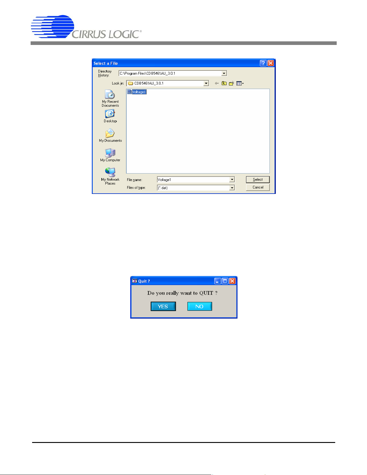
If Data from Disk is selected, a file selection window will appear as shown in Figure 5. The user can select a presaved data file for further analysis using time domain, FFT, and histogram plots in the Data Collection window of the
software.
10 DS661DB1
Page 11
CDB5461AU
Figure 5. Selecting a Data File for Further Analysis
2.3.2 Quit
Quit allows the user to exit the evaluation software. Upon selecting Quit, a message windows appears that verifies
whether exiting the evaluation software is desired. See Figure 6.
Figure 6. Quit Window
DS661DB1 11
Page 12

CDB5461AU
2.3.3 Menu
Except for the Start-up window, Menu allows 7 selection options, Setup window, Calibration window, Conversion
window, Pulse Rate window, Data Collection window, EEPROM window and Debug window. Each window provides
a means to evaluate the different functionalities and performances of the CS5461A. See Figure 7.
Figure 7. Menu Pull-down Options
2.4 Setup Window
The evaluation software provides access to the CS5461A's internal registers in the Setup window (Figure 8). The
user can enter the Setup window by pulling down Menu and selecting the Setup Window menu item, or by pressing
<F2> on the keyboard.
In the Setup window, all of the CS5461A's registers are displayed in hexadecimal notation, an d also decoded to provide easier readability. Refer to the CS5461A data sheet for information on register functionality and descriptions.
12 DS661DB1
Page 13

CDB5461AU
Figure 8. Setup Window
2.4.1 Refresh Screen Button
The Refresh Screen button will update the contents of the screen by reading all the register values from the
CS5461A device. It is a good idea to press th e Refresh Screen button when entering the Setup window, or after
modifying any registers to reflect the current status of the device.
2.4.2 Reset DUT Button
The R eset DUT button will hardware reset the CS5461A. The CS5461A will perform a reset as discussed in the
CS5461A data sheet. After the hardware reset to CS5461A, the screen contents will be automatically refreshed with
the updated status of the CS5461A device.
2.4.3 CS5461A Crystal Frequency
The CS5461A accepts a wide range of crystal input frequencies, and can therefore run at many different sample
rates. The crystal frequency being used on the CS5461A shoul d be entered in this field to provide accurate fre quency calculation in the FFT window. This will also help the software decide which functions can be performed reliably
with the evaluation system.
DS661DB1 13
Page 14

CDB5461AU
2.4.4 Configuration Register Panel
In the Configuration Register panel, the contents of the Configuration register can be modified by typing a hexadecimal value in the HEX: field, or by changing any of the values below the HEX: field to the desired settings. Although
the CDB5461AU software allows the user to modify any of the bits in the Configuration register, changing certain
bits may cause the software and board to behave erratically. For the evaluation system to function properly, the In-
terrupt Output field should be set to the default, Active Low setting, and E1, E2 Function field should be set to the
default Normal. This applies only to the CDB5461AU evaluation system, and not to the CS5461A chip itself.
2.4.5 Mask Register/Status Register Panel
The Mask and Status registers are displayed in hexadecimal and decoded in this box to indicate each bit's function.
The Mask register can be modified by typing a value in the HEX: field, or by checking the appropriate check boxes
for the bits that are to be masked. The Status register cannot be directly modified. It can only be reset b y pressing
the Clear Status Register button. The HEX: field for this register, and the associated “lamps” are for display only. A
lamp that is on means that the corresponding bit in the Status Register is set (except the Invalid Command bit, which
is inverted). The value present in the Mask register may be changed by the software during certain operations to
provide correct functionality of the CDB5461AU board.
2.4.6 Cycle Count / PulseRateE / PulseWidth / VSAGlevel / VSAGduration Registers
These fields display the values of the corresponding register in both hexad ecimal and decimal format. Each register
can be modified by typing a value in the corresponding Value: or HEX: field.
2.4.7 Control Register
The Control register contains various bits used to activate or terminate various features of the CS5461A. Refer to
the CS5461A data sheet for descriptions of these b its. The user is able to set or clear each bit in dividually. The value
of the Control register is displayed in the HEX: field. Most of the Control register bits are reserved or unused. Only
the usable bits are displayed in the Setup window.
14 DS661DB1
Page 15
CDB5461AU
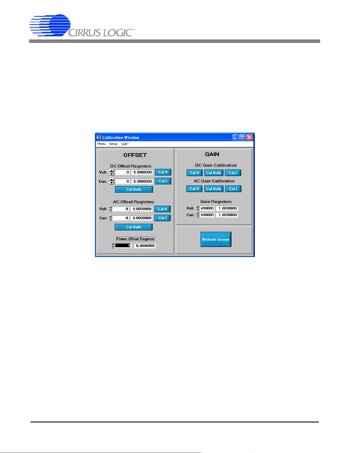
2.5 Calibration Window
The Calibration window is used to display and write to the CS5461A Offset and Gain calibration registers. The user
is also able to initiate the CS5461A's calibration sequences th at are used to set the calibra tion values. Both AC and
DC calibrations can be run for offset and gain, for either the voltage channel or the current channel, or both simultaneously. The user should refer to the CS5461A data sheet for more details on calibration.
The Refresh Screen button will update the contents of the window by reading all the register values from the
CS5461A device. It is a good idea to press the Refresh Screen button when entering the Calibration window, or after
modifying any registers to reflect the current status of the device.
Figure 9. Calibration Window
2.5.1 Offset & Gain Registers
In the Offset and Gain register panels, the offset and gain registers for bo th ch annels ar e d i splayed in he xa de cima l
and decimal. These registers can all be modified directly by typing the desired value in the hexadecimal display
fields. There are two types of offset registers: DC Offset and AC Offset. The AC Offset register only affects the RMS
register values. The DC and AC offset register values are two's complement numbers whose values ranges from
-1 to +1.
2.5.2 Performing Calibrations
Offset and gain calibrations can be performed on both the voltage and current channels of the CS5461A. It is generally a good idea to software reset the CS5461A before running calibrations because the values in the calibration
registers will affect the results of the calibration. A software reset will reset these registers back to the default values
of zero offset and unity gain. Offset calibration should be performed before gain calibration to ensure accurate results.
DS661DB1 15
Page 16

CDB5461AU
2.5.2.1 Offset Calibrations
1. Ground the channel(s) you want to calibrate directly at the chann el header(s). J17 and J22 for th e
voltage channel, and J24 and J26 for the current channel. The channel(s) could also be grounded
directly at the screw terminals.
2. Press the corresponding AC or DC offset calibrate button(s) (Cal V, Cal I, or Cal Both) in the Offset
panel.
3. The calibration value(s) will automatically update when the calibration is completed.
2.5.2.2 Gain Calibrations
1. Attach an AC or DC calibra tion signal to the screw terminals, and make sure the corresponding ch annel headers (J17, J22, J24, and J26) are set to the Input position.
2. Press the corresponding AC or DC gain calibrate button(s) (Cal V, Cal I, or Cal Both) in the Gain
Panel.
3. The calibration value(s) will automatically update when the calibration is completed.
The Calibration window also contains the Power Offset register display and adjustment fields . The user can read
and write the value in the Power Offset register.
16 DS661DB1
Page 17

CDB5461AU
2.6 Conversion Window
The Conversion window shown in Figure 10 allows the user to se e the results of single and continuo us conversions,
perform data averaging, utilize the power-saving modes of the CS5461A, and reset the CS5461A's serial port. The
Conversion window can be accessed by pulling down the Menu option, and selecting Conversion Window, or by
pressing <F4>.
Figure 10. Conversion Window
2.6.1 Single Conversion Button
By pressing this button, single conversions will be performed. After a single conversion is complete, the Result data
column will be updated with the values present in each data register.
2.6.2 Continuous Conversion Button
By pressing this button, continuous conversions will be performed until the user presses the Stop button. After each
conversion is complete, the Result data column will be updated with the values present in each data register. The
Mean and Standard Deviation columns will be updated every N cycles, where N is the number in the Samples to
Average: box. It may take many collection cycles after pressing the Stop button before the data actually stops being
collected.
2.6.3 Standby & Sleep Mode Buttons
When these buttons are pressed, the CS5461A device will enter either Standby or Sleep power-saving mode. To
return to normal mode, press the Power Up button.
DS661DB1 17
Page 18
CDB5461AU
2.6.4 Power Up Button
This button is used to send the Power-up/Halt command to the CS5461A. The device will return to normal operating
mode and halt any conversions that are bein g pe rf ormed at the time.
2.6.5 Temperature Settings Window
The Temperature Settings win dow is us ed to adju st the C S5461A’s Temp erature Offset r egister (T
perature Gain register (T
(°F) and to improve temperature measurement ac curacy. Refer to the CS5 461A data sheet fo r the details of the Onchip Temperature Sensor.
) to convert the Temperature Register (T) from a Celsius scale (°C) to a Fahrenheit scale
gain
offset)
and Tem-
2.6.6 Write Data to File Window
This window provides a means to write the conversion result data to a .txt file for later analysis or print out. The file
path and name will be shown in Filename field. The Open File button is used to open a new or existing .txt file for
writing data. Each time the Write Data button is pressed, the result data is written to the file and the Number of Lines
Written field will be incremented by 1.
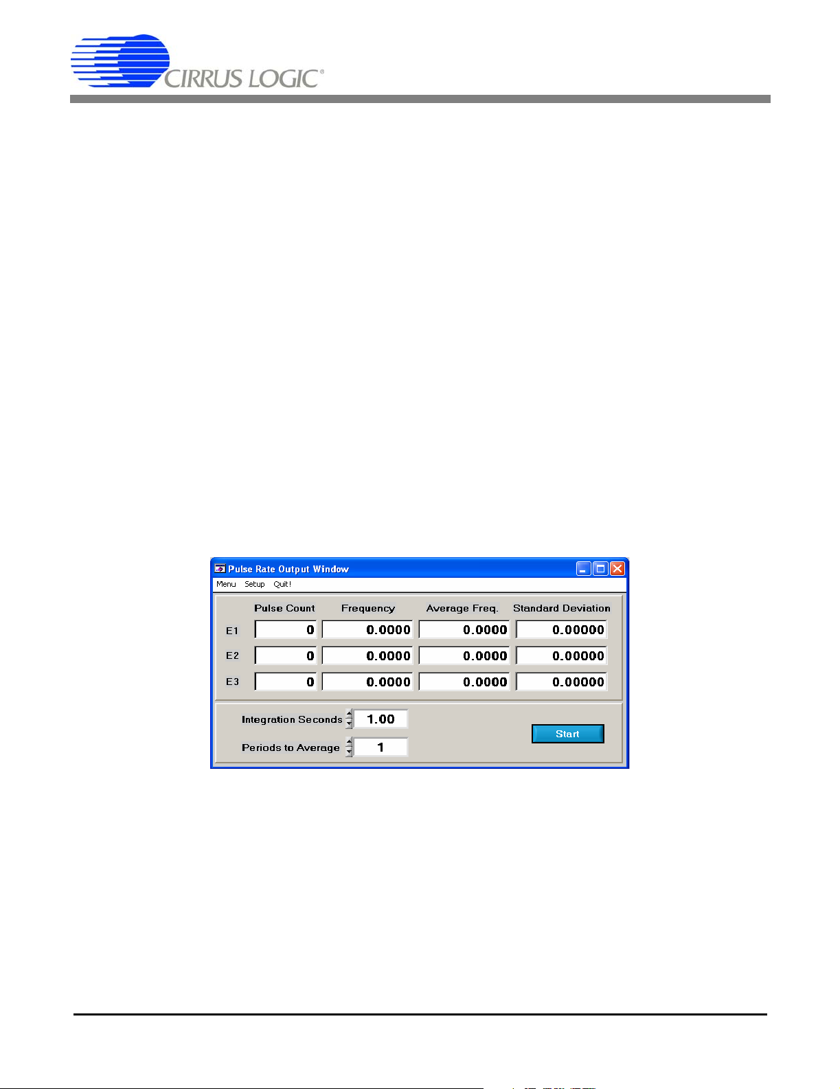
2.7 Pulse Rate Window
The CS5461A features a pulse-rate energy output. The CDB5461AU has the capability to demonstrate the functionality of this output in the Pulse Rate Output window shown in Figure 11. The Pulse Rate Output window can be accessed by pressing <F5>, or by pulling down Menu, and selecting Pulse Rate Window.
Figure 11. Pulse Rate Output Window
2.7.1 Integration Seconds Field
This box allows the user to select the length of time over which pulses will be collected.
2.7.2 Periods to Average Field
This box allows the user to average a number of integration periods.
18 DS661DB1
Page 19

CDB5461AU
2.7.3 Start Button
When the Start button is pressed, the CDB5461AU will capture pulse rate data according to the values in the Integration Seconds and Periods to Average fields. After each integration period, the Pulse Count and Frequency col-
umns will be updated. The Average Freq. and Standard Deviation columns will only be updated after all the
integrations have been collected. The software stops collecting da ta when the user presses the Stop button, or when
the data collection is complete. Due to speed limitations of the on-board microcontroller, some higher pulse rates
cannot be accurately collected.
2.8 Data Collection Window
The Data Collection window (Figure 12, Fig ure 13, and Figure 14) allows the user to collect sample sets of data from
the CS5461A and analyze them using time domain, FFT, and histogram plots. The Data Collection window is accessible through the Menu pull-down, or by pressing <F6>.
Figure 12. Data Collection Window
2.8.1 Time Domain / FFT / Histogram Pull-down
This pull-down selects the type of data processing to perfor m on the collected data and display in the plot area. Refer
to the section on Analyzing Data for more information.
2.8.2 Config Button
This button will bring up the Configuration window, in which the user can modify the data collection specifications.
See the discussion of the Config window in this document.
DS661DB1 19
Page 20

CDB5461AU
2.8.3 Collect Button
This button will collect data from the CS5461A device to be analyzed in the plot area. See the section on Collecting
Data Sets for more information.
2.8.4 Output Button
This button will bring up a window in which the user can output the data to a file for later use, print out a plot, or print
out the entire screen. When saving data, only the data channel being displayed on the plot will be saved to a file.
2.8.5 Zoom Button
This button allows the user to zoom in on the plot b y selecting two points in the plot area. Press the Restore button
to return to the normal data plot, or press the Zoom button again to zoom in even further.
2.8.6 Channel Select Button
After data collection, Current and Voltage channel select buttons will appear below the graph, allowing the user to
choose the appropriate channel for display. In the Time Domain mode, an additional Overlay button will be present,
to allow the user to display all the channels on the same plot.
2.8.7 Config Window
The Config window allows the user to set up the data collection and analysis parameters.
2.8.7.1 Number of Samples
This field allows the user to select the number of samples to co llect – between 16 and 32768.
2.8.7.2 Average
When doing FFT processing, this field will determine the number of FFTs to average. FFTs will be collected and
averaged when the Collect button is pressed.
2.8.7.3 FFT Window
This field allows the user to select the type of windowing algorithm for FFT processing. Windowing algorithms include the Blackman, Blackman-Harris, Hanning, 5-term Hodie, and 7-term Hodie. The 5-term Hodie and 7-term Hod-
ie are windowing algorithms developed at Crystal Semiconductor.
2.8.7.4 Histogram Bin Width
This field allows for a variable bin width when plotting histograms of the collected data. Each vertical bar in the histogram plot will contain the number of output codes contained in this field. Increasing this number allows the user to
view histograms with larger input ranges.
2.8.7.5 Data to Collect
These 3 check boxes allow the user to select the data types that will be collected and returned to the PC for processing.
20 DS661DB1
Page 21

CDB5461AU
2.8.7.6 Cycle Count
The value in Cycle Count field will be written to the CS5461A’s Cycle Count register. Cycle Count determines the
length of one computation cycle. Cycle Count should be selected app ropria tel y acco rding to th e Data to Collect selection. For example, if the Data to Collect is instantaneous Current, Vo ltage, or Power, it is better to set Cycle Count
to 1. If the data to collect is RMS Current, RMS Voltage, or Average Power, Cycle Count should be set to a value
that makes one computation cycle to be a even multiple of the line frequency.
2.8.7.7 Accept Button
When this button is pressed, the current settings will be saved, and the user will return to the Data Collection window.
2.8.8 Collecting Data Sets
To collect a sample data set:
1. In the Data Collection Window, press the Config button to bring up the Configuration Window and
view the current settings.
2. Select the appropriate settings from the available options (see the section on the Configuration Window) and press the Accept button.
3. The Data Collection Window should still be visible. Press the Collect button to begin collecting data.
4. Once the data has been collected, it can be analyzed, printed, or saved to disk.
2.8.9 Retrieving Saved Data from a File
The CDB5461AU software allows the user to save data to a file, and retrieve it later when needed. To load a previously saved file:
1. Pull down the Setup option and select Disk. A file menu will appear.
2. Find the data file in the list and select it. Press the select button to return.
3. Go to the Data Collection Window, and press the Collect button.
4. The data from the file should appear on the screen. To select a different file, repeat the procedure.
2.8.10 Analyzing Data
The evaluation software provides three types of analysis tests: Time Domain, Frequency Domain, and Histogram.
The Time Domain analysis process acquires conversions to produce a plot of magnitude versus conversion sample
number. The Frequency Domain analysis process acquires conversions to produce a plot of magnitude versus frequency using the Fast-Fourier Transform (results up to Fs/2 are calculated and plotted). Also statistical noise calculations are calculated and displayed. The Histogram analysis test process acquires conversions to produce a
histogram plot. Statistical noise calculations are also calculated and displayed.
DS661DB1 21
Page 22
CDB5461AU
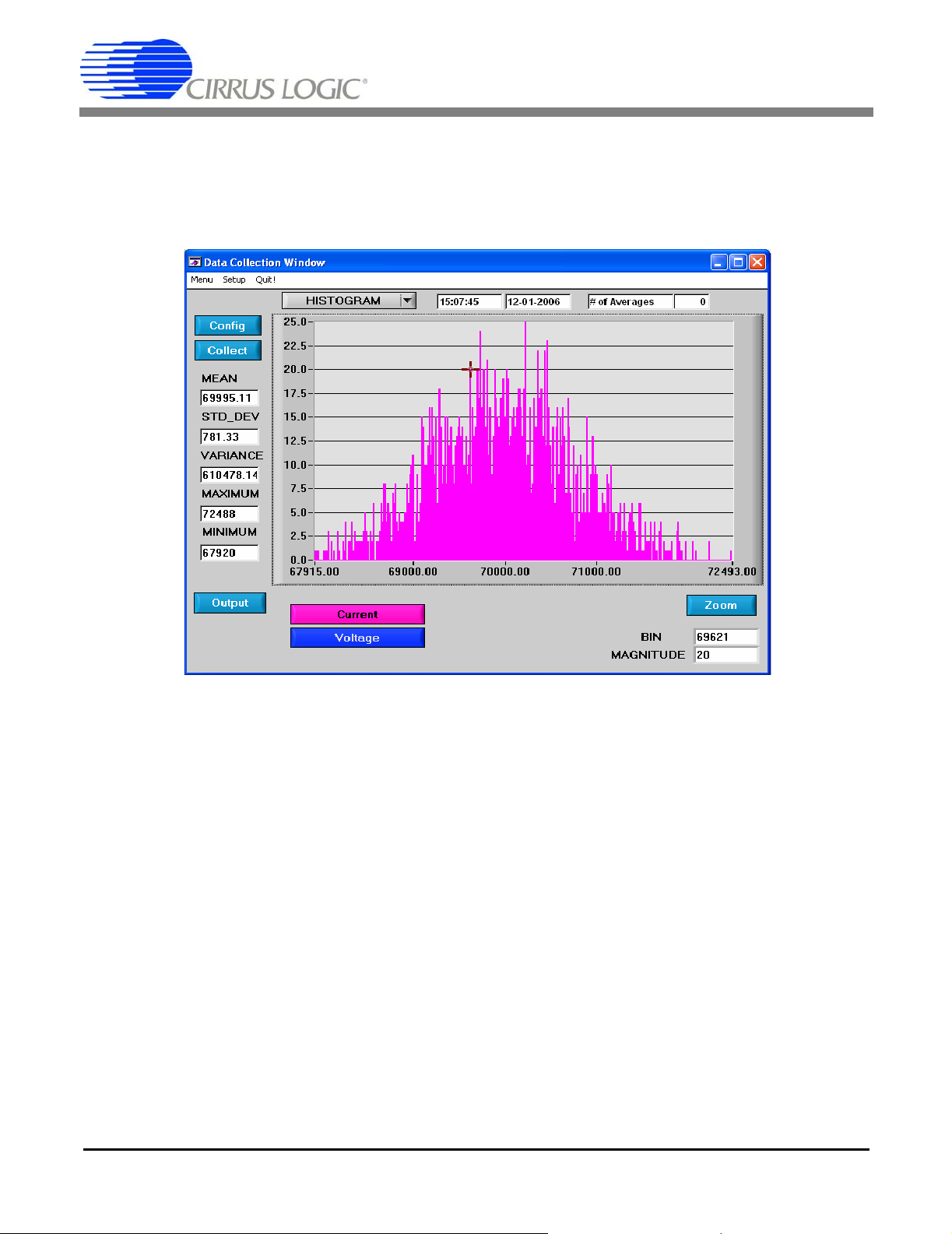
2.8.11 Histogram Information
The following is a description of the indicators associated with Histogram analysis. Histograms can be plotted in the
Data Collection window by setting the Time Domain / FFT / Histogram selector to Histogram (Figure 13).
Figure 13. Histogram Analysis
2.8.11.1 Bin
Displays the x-axis value of the cursor on the Histogram.
2.8.11.2 Magnitude
Displays the y-axis value of the cursor on the Histogram.
2.8.11.3 Mean
Indicator for the mean of the data sample set. The mean is calculated using the following formula:
n 1–
Xi
∑
i 0=
Mean
=
----------------
n
22 DS661DB1
Page 23

CDB5461AU
2.8.11.4 STD_DEV
Indicator for the standard deviation of the collected da ta set. The standard deviation is calculated using the following
formula:
StdDev
-------------------------------------------- -=
n 1–
∑
i 0=
Xi Mean–()
2
n
2.8.11.5 Variance
Indicator for the variance of the current data set. The variance is calculated using the following formula:
Var
n 1–
Xi Mean–()
∑
i 0=
-------------------------------------------- -
=
2
n
2.8.11.6 Maximum
Indicator for the maximum value of the collected data set.
2.8.11.7 Minimum
Indicator for the minimum value of the collected data set.
DS661DB1 23
Page 24

CDB5461AU
2.8.12 Frequency Domain Information
The following describe the indicators associated with FFT (Fast Fourier Transform) analysis. FFT data can be plotted in the Data Collection window by setting the Time Domain / FFT / Histogram selector to FFT (Figure 14).
Figure 14. FFT Analysis
2.8.12.1 Frequency
Displays the x-axis value of the cursor on the FFT display.
2.8.12.2 Magnitude
Displays the y-axis value of the cursor on the FFT display.
2.8.12.3 S/PN
Indicator for the signal-to-peak noise ratio (decibels).
2.8.12.4 SINAD
Indicator for the signal-plus-noise-plus- dis tor tio n to nois e- plu s- dis tor tio n ra tio (de cib els ).
2.8.12.5 S/D
Indicator for the signal-to-distortion ratio, 4 harmonics are used in the calculations (decibels).
24 DS661DB1
Page 25

CDB5461AU
2.8.12.6 SNR
Indicator for the signal-to-noise ratio, first 4 harmonics are not included (decibels).
2.8.12.7 Fs-Pdb
Indicator for the full-scale to signal ratio (decibels).
2.8.13 Time Domain Information
The following controls and indicators are associated with Time Domain analysis. Time Domain data can be plotted
in the Data Collection window by setting the Time Domain / FFT / Histogram selector to Time Domain (Figure 15).
Figure 15. Time Domain Analysis
2.8.13.1 Count
Displays current x-position of the cursor on the time domain display.
2.8.13.2 Magnitude
Displays current y-position of the cursor on the time domain display.
2.8.13.3 Maximum
Indicator for the maximum value of the collected data set.
DS661DB1 25
Page 26

CDB5461AU
2.8.13.4 Minimum
Indicator for the minimum value of the collected data set.
2.9 EEPROM Window
CDB5461AU has an “Auto-boot” Demo feature for the serial EEPROM, which means CDB5461AU can operate independently without connecting to a PC. The CDB5461AU GUI software also provides an EEPROM window for
reading/writing the serial EEPROM (Figure 16).
Figure 16. EEPROM Window
The Bytes to Read/Write field allows the user to define the number of bytes to be read or written.
2.9.1 Read EEPROM
After pressing the Read button, the number of bytes indicated in the Bytes to Read/Write field, starting from address
0x00 will be read from EEPROM and displayed in the EEPROM table in Hexadecimal format.
2.9.2 Write EEPROM
Starting from address 0x00, enter into the EEPROM table the bytes to be written. Pressing the Write button, the
bytes in the EEPROM table will be written to the EEPROM.
2.9.3 Debug Window
The Debug window provides the user a way to access the CS5461A registers and send commands to the device
directly (Figure 17). Refer to the CS5461A data she et for m or e de ta ils.
26 DS661DB1
Page 27

Figure 17. Debug Window
CDB5461AU
DS661DB1 27
Page 28
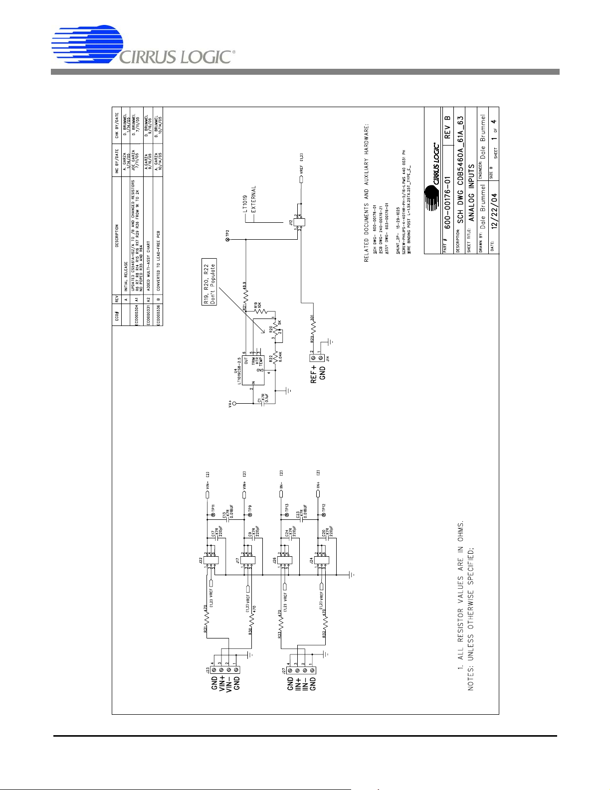
3. SCHEMATICS
CDB5461AU
Figure 18. Analog Inputs
28 DS661DB1
Page 29

CDB5461AU
Figure 19. CS546x and Socket
DS661DB1 29
Page 30

CDB5461AU
Figure 20. Microcontroller and USB Interface
30 DS661DB1
Page 31
CDB5461AU
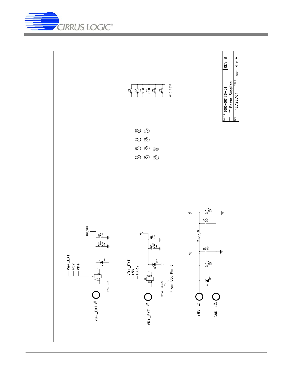
Figure 21. Power Supplies
DS661DB1 31
Page 32

4. LAYOUT
CDB5461AU
Figure 22. Top Silk Screen
32 DS661DB1
Page 33

CDB5461AU
Figure 23. Topside Layer
DS661DB1 33
Page 34

CDB5461AU
Figure 24. Bottomside Layer
34 DS661DB1
Page 35

CDB5461AU
Figure 25. Bottom Silk Screen
DS661DB1 35
Page 36

CDB5461AU
Contacting Cirrus Logic Support
For all product questions and inquiries contact a Cirrus Logic Sales Representative.
To find one nearest you go to www.cirrus.com
IMPORTANT NOTICE
Cirrus Logic, Inc. and it s su bsi di ar i es ( " Ci r ru s" ) beli ev e that th e i nfo r mat i on co nta i ne d in thi s docu ment is acc ura t e and r el iable. However, the inf o rmat io n i s subj ec t
to change without not ice and i s provi ded "AS I S" without warrant y of any kind (ex press or implie d). Cust omers are a dvised t o obtain the latest version of relevant
information to verify, before placing orders, that information being relied on is current and complete. All products are sold subject to the terms and conditions of sale
supplied at the time of order acknowledgment, including those pertaining to warranty, indemnification, and limitation of liability. No responsibility is assumed by Cirrus
for the use of this information, includ ing u se of this i nforma tion a s the basis for m anu facture or sa le of a ny items, or for in fringement of patents or other rights of third
parties. This document is the property of Ci rru s and by furnishing this information, Cirrus gran ts no license, express or implied under any patents, mask work rights,
copyrights, trademarks, trade secrets or other intellectual property rights. Cirrus owns the copyrights associated with the information contained herein and gives consent for copies to be made of the information only for use within yo ur organization with respect to Cirrus integrated circuits or other products of Cirrus. This consent
does not extend to other copying such as copying for ge ne ral distribution, advertising or promotional purp ose s, or for crea ting any work for resale.
CERTAIN APPLICATIONS USING SEMIC ONDUCTOR P RODUCTS MAY I NVOL VE POTE NT I AL RI SKS OF DE ATH, PERSONAL INJURY, OR SEVERE P ROPERTY OR ENVIRONMENTAL DAMAGE ("CRITICAL APPLICATIONS"). CIRRUS PRODUCTS ARE NOT DESIGNED, AUTHORIZED OR WARRANTED FOR USE
IN AIRCRAFT SYSTEMS, MILITARY APPLICATIONS, PRODUCTS SURGICALLY IMPLANTED INTO THE BODY, AUTOMOTIVE SAFETY OR SECURITY DEVICES, LIFE SUPPORT PRODUCTS OR OTHER CRITICAL APPLICATIONS. INCLUSION OF CIRRUS PRODUCTS IN SUCH APPLICATIONS IS UNDERSTOOD
TO BE FULLY AT THE CUSTOMER'S RISK AND CIRRUS DISCLAIMS AND MAKES NO WARRANTY, EXPRESS, STATUTORY OR IMPLIED, INCLUDING THE
IMPLIED WARRANTIES OF MERCHANTABILITY AND FITNESS FOR PARTICULAR PURPOSE, WITH REGARD TO ANY CIRRUS PRODUCT THAT IS USED
IN SUCH A MANNER. IF THE CUSTOMER OR CUSTOMER'S CUSTOMER USES OR PERMITS THE USE OF CIRRUS PRODUCTS IN CRITICAL APPLICATIONS, CUSTOMER AGREES, BY SUCH USE, TO FULLY INDEMNIFY CIRRUS, ITS OFFICERS, DIRECTORS, EMPLOYEES, DISTRIBUTORS AND OTHER
AGENTS FROM ANY AND ALL LIABILITY, INCLUDING ATT ORNEYS' FEES AND COSTS, THAT MAY RESULT FROM OR ARISE IN CONNECTION WITH
THESE USES.
Cirrus Logic, Cirrus, and the Cirrus Lo g ic lo go d esi gn s ar e trademarks of Cirrus Logic, Inc. All other brand an d product names in this document may be trademarks
or service marks of their respective owners.
Windows, Windows 2000, and Window s XP ar e re giste re d tra de m a rks of M icroso ft Corp or ation.
SPI is a trademark of Motorola, Inc.
CVI is a trademark of National Instruments Corporation.
36 DS661DB1
 Loading...