

Page 1
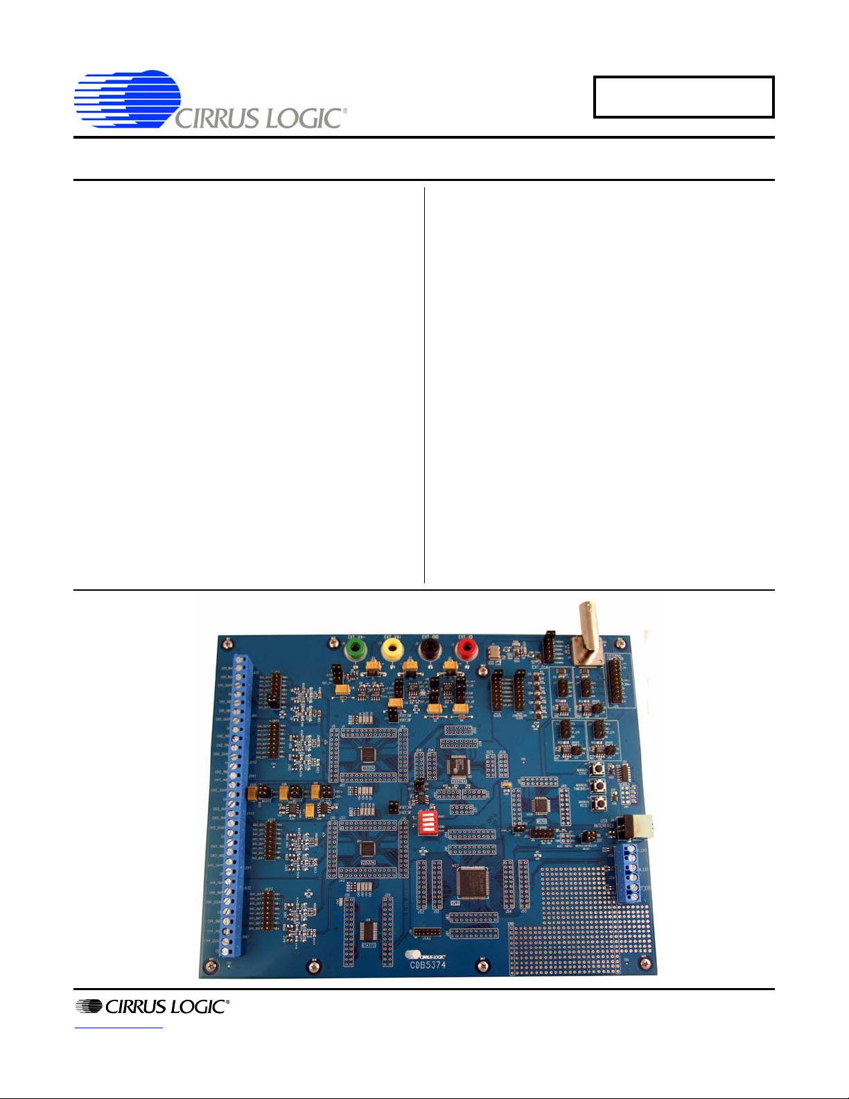
CDB5374
Multichannel Marine Seismic Evaluation System
Features
z Four-channel Seismic Acquisition Node
– CS5374 dual amplifier & ∆Σ modulator (2x)
– CS5376A quad digital filter (1x)
– CS4373A ∆Σ test DAC (1x)
– Precision voltage reference
– Clock recovery PLL
z On-board Microcontroller
– SPI™ interface to digital filter
– USB communication with PC
z PC Evaluation Software
– Register setup & control
– FFT frequency analysis
– Time domain analysis
– Noise histogram analysis
General Description
The CDB5374 board is used to evaluate the functionality
and performance of the Cirrus Logic multichannel marine seismic chip set. Data sheets for the CS5374,
CS5376A, and CS4373A devices should be consulted
when using the CDB5374 evaluation board.
Screw terminals connect external differential hydrophone sensors to the analog inputs of the measurement
channels. An on-board test DAC creates precision differential analog signals for in-circuit performance testing
without an external signal source.
The evaluation board includes an 8051-type microcontroller with hardware SPI
The microcontroller communic ates with the digital filter
via SPI and with the PC evaluation software via USB.
The PC software controls register and coefficient initialization and performs time domain, histogram, and FFT
frequency analysis on captured data.
ORDERING INFORMATION
CDB5374 Evaluation Board
™ and USB serial interfaces.
www.cirrus.com
Copyright © Cirrus Logic, Inc. 2009
(All Rights Reserved)
JAN ‘09
DS862DB1
Page 2

REVISION HISTORY
Revision Date Changes
DB1 JAN 2009 Initial release.
CDB5374
Contacting Cirrus Logic Support
For all product questions and inquiries contact a Cirrus Logic Sales Re presentative. To find the one near est to you
go to www.cirrus.com
IMPORTANT NOTICE
Cirrus Logic, Inc. and its subsidiaries ("Cirru s") believe that the information contained in this document is accurate and reli a b le. However, the information is subject
to change without notice and is provided "AS IS" without warranty of any kind (express or implied). Customers are advised to obtain the latest version of relevant
information to verify, before placing or ders, that in formatio n be ing relied on is current and comple te. All products a re sold s ubj ect to the term s and conditions of sa le
supplied at the time of order acknow ledgment, includin g those pertaining to warranty, indemni fication, and limitatio n of liability. No responsibility is assumed by Cirrus
for the use of this information, including use of this information as the basis for manufacture or sale of any items, or for infringement of patents or other rights of third
parties. This document is the prop erty o f C irrus a nd b y furn ishing this inform ation, Cirru s grants no lice nse, expres s or implied under any patents, mask work rights,
copyrights, trade marks, trad e secrets or other int ellectual property r ights. Cirr us owns the co pyrights a ssociated wit h the inf ormation contained herein and gives
consent for copies to be made of the inform ation only for us e withi n your o rgani zation w ith resp ect to Cir rus in tegrate d circui ts or other p rodu cts of C irrus. This co nsent does not extend to other copying such as copying for general distribution, advertising or promotional purposes, or for creating any work for resale.
CERTAIN APPLICATIONS USING SEMICONDUCTOR PRODUCTS MAY INVOLVE POTENTIAL RISKS OF DEATH, PERSONAL INJURY, OR SEVERE PROPERTY OR ENVIRONMENTAL DAMAGE ("CRITICAL APPLICATIONS"). CIRRUS PRODUCTS ARE NOT DESIGNED, AUTHORIZED OR WARRANTED FOR
USE IN PRODUCTS SURGICALLY IMPLANTED INTO THE BODY, AUTOMOTIVE SAFETY OR SECURITY DEVICES, LIFE SUPPORT PRODUCTS OR OTHER
CRITICAL APPLICATIONS. INCLUSION OF CIRRUS PRODUCTS IN SUCH APPLICATIONS IS UNDERSTOOD TO BE FULLY AT THE CUSTOMER'S RISK
AND CIRRUS DISCLAIMS AND MAKES NO WARRANTY, EXPRESS, STATUTORY OR IMPLIED, INCLUDING THE IMPLIED WARRANTIES OF MERCHANTABILITY AND FITNESS FOR PARTICULAR PURPOSE, WITH REGARD TO ANY CIRRUS PRODUCT THAT IS USED IN SUCH A MANNER. IF THE CUSTOMER
OR CUSTOMER'S CUSTOMER USES OR PERMITS THE USE OF CIRRUS PRODUCTS IN CRITICAL APPLICATIONS, CUSTOMER AGREES, BY SUCH USE,
TO FULLY INDEMNI FY CIRRUS , ITS O FFICERS, DIRECTOR S, EMPLOY EES, DIST RIBUTORS AND OTHER AGENTS FROM ANY AND ALL LIABILI TY, INCLUDING ATTORNEYS' FEES AND COSTS, THAT MAY RESULT FROM OR ARISE IN CONNECTION WITH THESE USES.
Cirrus Logic, Cirrus, and the Cirrus Logic logo designs are trademarks of Cirrus Logic, Inc. All other brand and product names in this document may be trademarks
or service marks of their respective owners.
Windows, Windows XP, Windows 2000, and Windows NT are trademarks or registered trademarks of Microsoft Corporation.
Intel and Pentium are registered trademarks of Intel Corporation.
SPI is a trademark of Motorola, Inc.
I2C (I2C) is a registered trademark of Philips Semiconductor Corporation.
USBXpress is a registered trademark of Silicon Laboratorie s, Inc .
2 DS862DB1
Page 3

CDB5374
TABLE OF CONTENTS
REVISION HISTORY .................................................................................................................... 2
1. INITIAL SETUP ......................................................................................................................... 5
1.1 Kit Contents ............................... ... ... ... ....................................... ... ... .... ... ... ........................ 5
1.2 Hardware Setup ............................... ....................... ...................... ....................... .............. 5
1.2.1 Default Jumper Settings ............................. ... ... ... .... ... ... ... ... .... .............................. 6
1.2.2 Default DIP Switch Settings ............................................ ..................................... 8
1.3 Software Setup ................................... ... .... ... ... ... .... ... ........................................................ 9
1.3.1 PC Requirements ............................. ... ... .... ... ... ....................................... ... ... ... .... . 9
1.3.2 Seismic Evaluation Software Installation ...................................... ... .... ... ... ... ........ 9
1.3.3 USBXpress Driver Installation ............................................................................... 9
1.3.4 Launching the Seismic Evaluation Software .............................. ......................... 10
1.4 Self-testing CDB5374 ...................... ... ... .... ... ... ... .... ... ....................................... ... ... ... ... ... 11
1.4.1 Noise test ..... .... ... ... ... ....................................... ... .... ... ...................................... ... 11
1.4.2 Distortion Test .. ... ....................................... ... ... ... .... ... ... ... ... .... ... ......................... 12
2. HARDWARE DESCRIPTION ................................................................................................. 13
2.1 Block Diagram ................................................................................................................ 13
2.2 Analog Hardware ....................... ... ... ... ... .... ... ... ... .... ...................................... .... ... ... ... ... ... 14
2.2.1 Analog Inputs ...... ... ... .... ... ... ....................................... ... ... ... .... ... ... ...................... 14
2.2.2 Differential Amplifiers .............................................. ... ... ...................................... 16
2.2.3 Delta-Sigma Modulators ..................................................................................... 17
2.2.4 Delta-Sigma Test DAC ............................... ... ... ... .... ... ... ... ... .... ............................ 18
2.2.5 Voltage Reference .............. ... ... .... ...................................... .... ... ... ... .... ... ............ 19
2.3 Digital Hardware .............................................................................................................. 20
2.3.1 Digital Filter ......................................... ... .... ...................................... .... ... ... ... ...... 20
2.3.2 Interface CPLD ................................... ... .... ... ... ... .... ... ... ...................................... 22
2.3.3 Digital Control Signals ......................... ... .... ...................................... .... ... ... ... ... ... 24
2.3.4 Microcontroller ....................... ... .... ... ... ... .... ... ....................................... ... ... ... ... ... 24
2.3.5 Phase Locked Loop .................. .... ... ... ... ............................................................. 26
2.3.6 RS-485 Telemetry .. ... .......................................................................................... 28
2.3.7 UART Connection .. ... .... ... ... ... ... .... ...................................................................... 29
2.3.8 External Connector ................... .... ... ... ... .... ... ...................................................... 30
2.4 Power Supplies ................ ... ... .... ...................................... .... ... ... ... ... .... ... ... ... ................... 30
2.4.1 Analog Voltage Regulators ........... ... ... ... .... ... ... ... .... ... ...................................... ... 30
2.4.2 Digital Voltage Regulators .................................................................................. 31
2.5 PCB Layout ..................... ... ... .... ...................................... .... ... ... ... ... ................................ 32
2.5.1 Layer Stack ...... ... ... ... .... ... ....................................... ... ... ... ... .... ... ......................... 32
2.5.2 Differential Pairs ............................ ... ... ... .... ... ... ... ....................................... ... ... ... 32
2.5.3 Bypass Capacitors . ....................................... ... ... .... ... ... ... ................................... 33
2.5.4 Dual Row Headers .............................................................................................. 34
3. SOFTWARE DESCRIPTION .................................................................................................. 35
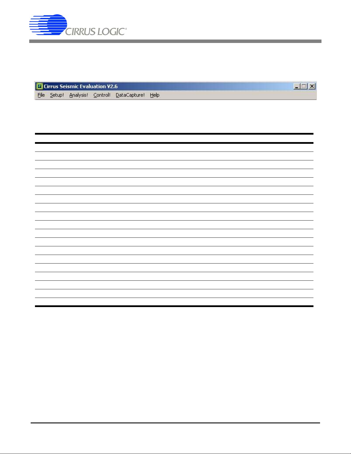
3.1 Menu Bar ................................... ... ... ... ... .... ...................................... .... ... ... ... .... ... ............ 35
3.2 About Panel ..................................................................................................................... 36
3.3 Setup Panel ..................................................................................................................... 37
3.3.1 USB Port ...... .... ... ... ....................................... ... ... .... ... ...................................... ... 38
3.3.2 Digital Filter ......................................... ... .... ... ....................................... ... ... ... ... ... 39
3.3.3 Analog Front End ...... .... ... ... ... ... .... ... ....................................... ... ... ... .... ... ... ... ... ... 40
3.3.4 Test Bit Stream ................... ... ... .... ... ....................................... ... ... ... .... ... ... ......... 40
3.3.5 Gain/Offset ............................. ... .... ... ... ....................................... ... ... .... ... ............ 41
3.3.6 Data Capture .......................... ....................................... ... ... .... ............................ 42
3.3.7 External Macros ..... ... .... ... ... ... ... ....................................... ... .... ... ... ... .... ............... 43
3.4 Analysis Panel ................................................................................................................. 44
3.4.1 Test Select ... .... ... ... ....................................... ... ... .... ... ... ...................................... 45
DS862DB1 3
Page 4

CDB5374
3.4.2 Statistics ........................ ... ... ....................................... ... ... ... .... ............................46
3.4.3 Plot Enable ............................. ... .... ... ... ... .... ... ....................................... ... ... ... ... ... 46
3.4.4 Cursor ....................... .... ... ....................................... ... ... ... ................................... 47
3.4.5 Zoom ...................................... ... .... ...................................... .... ... ... ... ...................47
3.4.6 Refresh ...................... .... ...................................... .... ... ... ... ... .... ............................ 47
3.4.7 Harmonics ..................................... ... ... ... .... ...................................... .... ... ... ... ... ... 47
3.4.8 Spot Noise ..................................................... ... ... .... ...................................... ... ... 47
3.4.9 Plot Error ....................................... ... ... ....................................... ... ... .... ... ............47
3.5 Control Panel ...................................................................................................................48
3.5.1 DF Registers ....... ... ... ....................................... ... .... ... ... ... ... ................................ 49
3.5.2 DF Commands .................................... ... .... ... ... ....................................... ... ... ... ... 49
3.5.3 SPI ......................... ... .... ...................................... .... ... ... ......................................49
3.5.4 Macros ...................... .... ...................................... .... ... ... ...................................... 50
3.5.5 GPIO ...... ... ... ....................................... ... .... ... ... ....................................... ... ... ... ... 50
3.5.6 Customize .... .... ...................................... .... ... ... ... ....................................... ... ... ... 51
3.5.7 External Macros ........ .... ... ... ... ....................................... ... ... .... ... ... ... ...................51
4. BILL OF MATERIALS ...........................................................................................................52
5. LAYER PLOTS ...................................................................................................................... 54
6. SCHEMATICS ........................................................................................................................ 62
LIST OF FIGURES
Figure 1. CDB5374 Block Diagram ...............................................................................................13
Figure 2. RC Filter External Components ..................................................................................... 16
Figure 3. CPLD Default Signal Assignments.................................................................................23
Figure 4. Differential Pair Routing.................................................................................................32
Figure 5. Quad Group Routing...................................................................................................... 33
Figure 6. Bypass Capacitor Placement.........................................................................................33
Figure 7. Dual-row Headers with Shorts ....................................................................................... 34
LIST OF TABLES
Table 1. Analog Inputs Default Jumper Settings........................................................ .... ... ... ... ... .... . 6
Table 2. VREF, SPI, SYNC, RESET Default Jumper Settings........................................................6
Table 3. Power Supplies Default Jumper Settings..........................................................................7
Table 4. Clock Inputs Default Jumper Settings ............................. .... ... ... ... ... .... ... ........................... 7
Table 5. RS-485 Default Jumper Settings.......................................................................................8
Table 6. DIP Switch Default Settings ..............................................................................................8
Table 7. Screw Terminal Input Connectors...................................................................................14
4 DS862DB1
Page 5

1. INITIAL SETUP
1.1 Kit Contents
The CDB5374 evaluation kit includes:
• CDB5374 Evaluation Board
• USB Cable (A to B)
• Software Download Information Card
The following are required to operate CDB5374, and are not included:
• Bipolar Power Supply with Banana Jack Outputs (+/-12 V @ 300 mA)
• Banana Jack Cables (4x)
• PC Running Windows 2000 or XP with an Available USB Port
• Internet Access to Download the Evaluation Software
CDB5374
1.2 Hardware Setup
To set up the CDB5374 evaluation board:
• Set all jumpers and DIP switches to their default settings (see next sections).
• With power off, connect the CDB5374 power inputs to the power supply outputs.
VA- = -12 V
VA+ = +12 V
GND = 0 V
VD = +12 V
• Connect the USB cable between the CDB5374 USB connector and the PC USB port.
• Proceed to the Software Setup section to install the evaluation software and USB driver.
DS862DB1 5
Page 6
1.2.1 Default Jumper Settings
DAC_OUT+ 1 **2INA+
DAC_OUT- 3 **4INA-
DAC_OUT- 5 ---------- 6INBDAC_OUT+ 7 ---------- 8INB+
DAC_BUF+ 9 ---------- 10 INA+
DAC_BUF- 11 ---------- 12 INA-
DAC_BUF- 13 **14 INB-
DAC_BUF+ 15 **16 INB+
BNC_IN+ 17 **18 INA+
BNC_IN- 19 **20 INA-
BNC_IN- 21 **22 INB-
BNC_IN+ 23 **24 INB+
CDB5374
J27, J227, J327, J427
CH1, CH2, CH3, CH4
Analog Input Selections
Table 1. Analog Inputs Default Jumper Settings
J519, J19, J20
Voltage Reference Jumpers
VREF+ 1 ---------- 2
VREF- 3 ---------- 4
J56
SYNC Source Selection
SYNC_IO 1 ---------- 2 SYNC
Table 2. VREF, SPI, SYNC, RESET Default Jumper Settings
EECS 3 **4 SSI
J43
SPI Chip Select Input
SSI 1 ---------- 2 SSI
J58
RESET Source Selection
RST_PB 1 ---------- 2
RST_EXT 3 ---------- 4
6 DS862DB1
Page 7
CDB5374
J10
VA- Voltage Selection
-2.5VA 1 ---------- 2
GND 3 **4
EXT_VA- 5 **6
J12
VD Input Voltage Source
EXT_VA+ 1 **2
EXT_VD 3 ---------- 4
J22
VD Voltage Selection
+3.3VD 1 ---------- 2
EXT_VD 3 **4
Table 3. Power Supplies Default Jumper Settings
J11
VA+ Voltage Selection
+2.5VA 1 ---------- 2
+5VA 3 **4
EXT_VA+ 5 **6
J13
VCORE Input Voltage Source
EXT_VA+ 1 **2
EXT_VD 3 ---------- 4
J21
VCORE Voltage Selection
+3.3VD 1 ---------- 2
+2.5VD 3 **4
EXT_VD 3 **4
J16
PLL Input Clock Selection
32.768 MHz 1 ---------- 2
16.384 MHz 3 **4
8.192 MHz 5 **6
4.096 MHz 7 **8
2.048 MHz 9 **10
1.024 MHz 11 **12
Table 4. Clock Inputs Default Jumper Settings
DS862DB1 7
CPLD, Microcontroller
Input Clock Selections
32.768 MHz 1 ---------- 2
16.384 MHz 3 **4
8.192 MHz 5 **6
4.096 MHz 7 **8
2.048 MHz 9 **10
1.024 MHz 11 **12
CLK_EXT 13 **14
J17, J18
15 **16
Page 8
CDB5374
J15
I2C Data
SDA+ 1 **2
SDA- 3 **4
SDA 5 **6
GND 7 **8
J24
Clock Source
CLK+ 1 **2
CLK- 3 **4
CLK_I/O 5 **6
GND 7 **8
J14
I2C Clock
SCL+ 1 **2
SCL- 3 **4
SCL 5 **6
GND 7 **8
J23
I2C Clock Driver Enable
GND 1 ---------- 2
VD 3 **4
J25
Sync Source
SYNC+ 1 **2
SYNC- 3 **4
SYNC_I/O 5 **6
GND 7 **8
J33
Clock Driver Enable
GND 1 ---------- 2
VD 3 **4
Table 5. RS-485 Default Jumper Settings
1.2.2 Default DIP Switch Settings
BOOT 1 *-2
LGND 5 *-6
OFST 7 -*8
Table 6. DIP Switch Default Settings
J34
Sync Driver Enable
GND 1 ---------- 2
VD 3 **4
S5
* = down, - = up
3 *-4
8 DS862DB1
Page 9

1.3 Software Setup
1.3.1 PC Requirements
The PC hardware requirements for the Cirrus Seismic Evaluation system are:
CDB5374
• Windows XP®, Windows 2000™, Windows NT
®
•Intel® Pentium® 600MHz or higher microprocessor
• VGA resolution or higher video card
• Minimum 64MB RAM
• Minimum 40MB free hard drive space
1.3.2 Seismic Evaluation Software Installation
Important: For reliable USB communication, the USBXpress® driver must be installed after the Seismic
Evaluation Software installation but before launching the application. The USBXpress driver files are in-
cluded in a sub-folder as part of the installation.
To install the Cirrus Logic Seismic Evaluation Software:
• Go to the Cirrus Logic Industrial Software web page (http://www.cirrus.com/industrialsoftware
the link for “Cirrus Seismic Evaluation GUI” to get to the download page and then click the link for “Cir-
rus Seismic Evaluation GUI Release Vxx” (xx indicates the version number).
• Read the software license terms and click “Accept” to download the “SeismicEvalGUI_vxx.zip” file to
any directory on the PC.
• Unzip the downloaded file to any directory and a “Distribution\Volume1” sub-folder containing the installation application will automatically be created.
• Open the “Volume1” sub-folder and run “setup.exe”. If the Seismic Evaluation Software has been previously installed, the uninstall wizard will automatically remove the previous version during install.
• Follow the instructions presented by the Cirrus Seismic Evaluation Installation Wizard. The default installation location is “C:\Program Files\Cirrus Seismic Evaluation”.
). Click
An application note, AN271 - Cirrus Seismic Evaluation GUI Installation Guide, is available from the Cirrus
Logic web site with step-by-step instructions on installing the Seismic Evaluation Software.
1.3.3 USBXpress Driver Installation
Important: For reliable USB communication, the USBXpress driver must be installed after the Seismic
Evaluation Software installation but before launching the application. The USBXpress driver files are in-
cluded in a sub-folder as part of the installation.
The Cirrus Logic Seismic Evaluation Software communicates with CDB5374 via USB using the USBXpress driver from Silicon Laboratories (http://www.silabs.com
files are included as part of the installation package.
To install the USBXpress driver (after installing the Seismic Evaluation Software):
• Connect CDB5374 to the PC through an available USB port and apply power. The PC will detect
DS862DB1 9
). For convenience, the USBXpress driver
Page 10

CDB5374
CDB5374 as an unknown USB device.
• If prompted for a USB driver, skip to the next step. If not, using Windows Hardware Device Manager
go to the properties of the unknown USB API device and select “Update Driver”.
• Select “Install from a list or specific location”, then select “Include this location in the search” and then
browse to “C:\Program Files\Cirrus Seismic Evaluation\Driver\”. The PC will recognize and install the
USBXpress device driver.
• After driver installation, cycle power to CDB5374. The PC will automatically detect it and add it as a
USBXpress device in the Windows Hardware Device Manager.
An application note, AN271 - Cirrus Seismic Evaluation GUI Installation Guide, is available from the Cirrus
Logic web site with step-by-step instructions on installing the USBXpress driver.
1.3.4 Launching the Seismic Evaluation Software
Important: For reliable USB communication, the USBXpress driver must be installed after the Seismic
Evaluation Software installation but before launching the application. The USBXpress driver files are in-
cluded in a sub-folder as part of the installation.
To launch the Cirrus Seismic Evaluation Software, go to:
• Start
or:
• C:\Program Files\Cirrus Seismic Evaluation\SeismicGUI.exe
For the most up-to-date information about the software, please refer to its help file:
• Within the software: Help
or:
• C:\Program Files\Cirrus Seismic Evaluation\SEISMICGUI.HLP
Ö
Programs Ö Cirrus Seismic Evaluation Ö Cirrus Seismic Evaluation
Ö
Contents
10 DS862DB1
Page 11
CDB5374
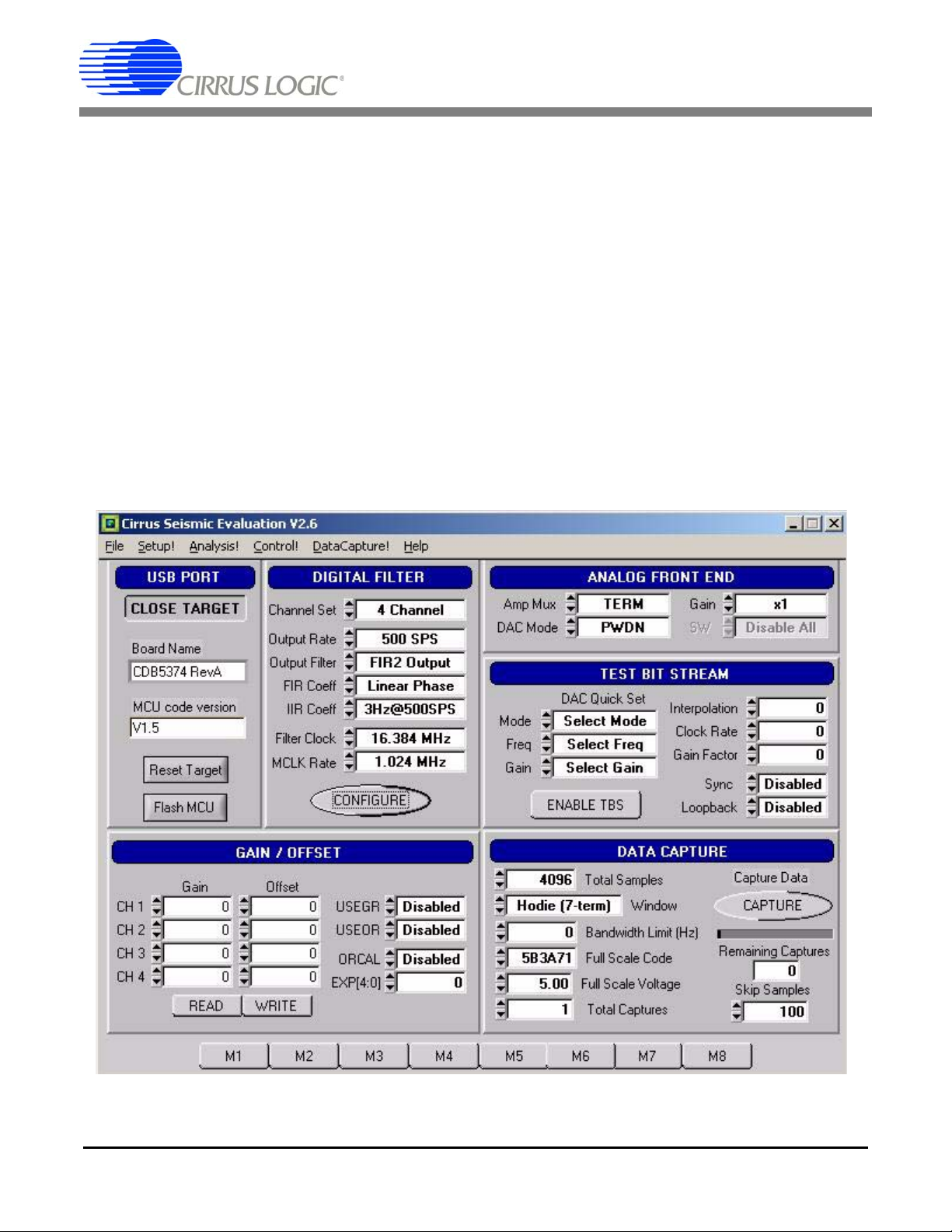
1.4 Self-testing CDB5374
Noise and distortion self-tests can be performed once hardware and software setup are complete.
First, initialize the CDB5374 evaluation system:
• Launch the evaluation software and apply power to CDB5374.
• Click ‘OK’ on the About panel to get to the Setup panel.
• On the Setup panel, select Open Target on the USB Port sub-panel.
• When connected, the Board Name and MCU code version will be displayed.
1.4.1 Noise test
Noise performance of the measurement channel can be tested as follows:
• Set the controls on the Setup panel to match the picture:
DS862DB1 11
Page 12
• Once the Setup panel is set, select Configure on the Digital Filter sub-panel.
• After digital filter configuration is complete, click Capture to collect a data record.
• Once the data record is collected, the Analysis panel is automatically displayed.
• Select Noise FFT from the Test Select control to display the calculated noise statistics.
• Verify the noise performance (S/N) is 121 dB or better.
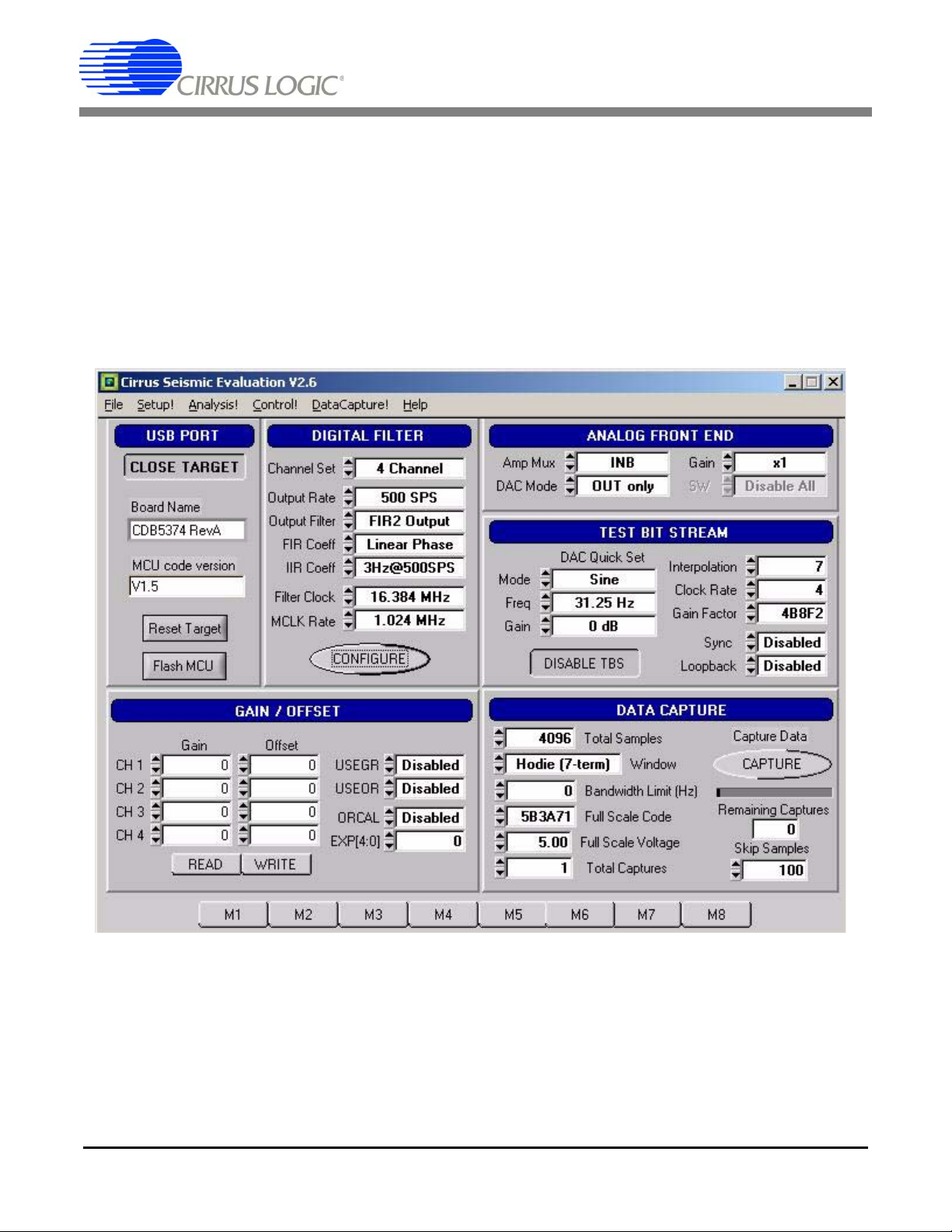
1.4.2 Distortion Test
• Set the controls on the Setup panel to match the picture:
CDB5374
• Once the Setup panel is set, select Configure on the Digital Filter sub-panel.
• After digital filter configuration is complete, click Capture to collect a data record.
• Once the data record is collected, the Analysis panel is automatically displayed.
• Select Signal FFT from the Test Select control to display the calculated signal statistics.
• Verify the distortion performance (S/D) is 108 dB or better.
12 DS862DB1
Page 13
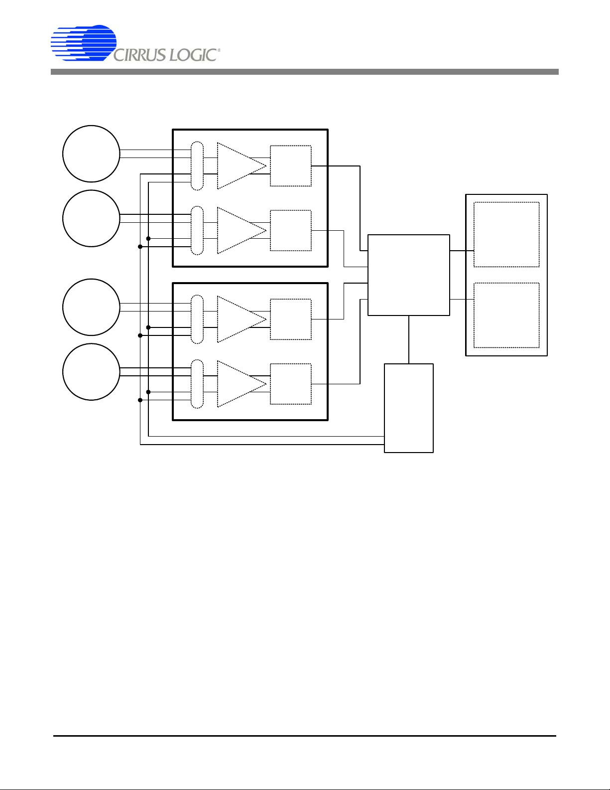
2. HARDWARE DESCRIPTION
2.1 Block Diagram
Hydrophone
Sensor
M
U
X
AMP
CDB5374
CS5374
DS
Modulator
Hydrophone
Sensor
Hydrophone
Sensor
Hydrophone
Sensor
M
U
X
M
U
X
M
U
X
AMP
AMP
AMP
DS
Modulator
CS5374
DS
Modulator
DS
Modulator
CS5376A
Digital Filter
CS4373A
Test
DAC
Microcontroller
or
Configuration
EEPROM
System
Telemetry
Figure 1. CDB5374 Block Diagram
Major blocks of the CDB5374 evaluation board include:
• CS5374 Dual Amplifier & ∆Σ Modulator (2x)
• CS5376A Quad Digital Filter
• CS4373A ∆Σ Test DAC
• Precision Voltage Reference
• Interface CPLD
• Microcontroller with USB
• Phase Locked Loop
• RS-485 Transceivers
• Voltage Regulators
DS862DB1 13
Page 14
CDB5374
2.2 Analog Hardware
2.2.1 Analog Inputs
2.2.1.1 External Inputs - INA, INB, BNC
External signals into CDB5374 are typically from piezoelectric hydrophones, which are high-impedance
sensors optimized to measure pressure in marine applications.
External signals connect to CDB5374 through screw terminals on the left side of the PCB. For each channel (CH1, CH2, CH3, CH4), these screw terminals make connections to two external differential inputs,
INA and INB. In addition, GND and GUARD connections are provided for connecting sensor cable shields,
if present.
Signal Input Screw Terminal
CH1 INA J32
CH1 INB J41
CH2 INA J232
CH2 INB J241
CH3 INA J332
CH3 INB J341
CH4 INA J432
CH4 INB J441
Table 7. Screw Terminal Input Connectors
2.2.1.2 GUARD Output, GND Connection
The CS5374 hydrophone amplifier provides a GUARD signal output designed to actively drive the cable
shield of a high impedance sensor with the common mode voltage of the sensor differential signal. This
GUARD output on the cable shield minimizes leakage by minimizing the voltage differential between the
sensor signal and the cable shield.
The GUARD signal is output to screw terminals on the left side of the PCB an d a separate GND connection screw terminal for each channel is also provided if a ground connection to the sensor cable shield is
preferred.
2.2.1.3 Internal Inputs - DAC_OUT, DAC_BUF
The CS4373A test DAC has two high-performance differential test outputs, a precision output
(DAC_OUT) and a buffered output (DAC_BUF). These test outputs can be connected to the INA or INB
inputs of any channel through the input selection jumpers.
By default, CDB5374 is populated with passive RC filter components on the INA inputs, and no filter components on the INB inputs (though the component footprints are present on the INB inputs). Because the
CS4373A precision output will not tolerate significant loading, on CDB5374 the DAC_OUT signal should
only jumper to the INB inputs. The CS4373A buffered outputs are less sensitive to the RC filter load and
DAC_BUF can be jumper-ed to either the INA or INB inputs.
14 DS862DB1
Page 15

CDB5374
2.2.1.4 Input Protection
Sensor inputs must have circuitry to protect the analog electronics from voltage spikes as hydrophones
can produce large voltage spikes if located near an air gun source.
Discrete switching diodes quickly clamp the analog inputs to the power supply rails when the input voltage
spikes. These diodes are reverse biased in normal operation and have low reverse bias leakage and capacitance characteristics to maintain high linearity on the analog inputs.
Specification Value
Dual Series Switching Diode - ON Semiconductor BAV99LT1
Surface Mount Package Type SOT-23
Non-Repetitive Peak Forward Current (1 µs, 1 ms, 1 s)
Reverse Bias Leakage (25 C to 85 C)
Reverse Bias Capacitance (0 V to 5 V) 1.5 pF - 0.54 pF
2.2.1.5 Input RC Filters
Following the diode clamps is an RC filter network that bandwidth limits the sensor inputs into the amplifiers to “chop the tops off” residual voltage spikes not clamped by the discrete diodes. In addition , all Cirrus
Logic component ICs have built in ESD protection diodes guaranteed to 2000 V HBM / 200 V MM (JEDEC
standard). The small physical size of these ESD diodes restricts their current capacity to 10 mA.
2.0 A, 1.0 A, 500 mA
0.004 µA - 0.4 µA
For marine applications that use the CS3302A amplifier, the inherent capa citance of the piezoelectric sensor is combined with large resistors to create an analog high-pass RC filter to eliminate the low-frequency
components of ocean noise.
Marine Differential Filter Specification Value
Hydrophone Group Capacitance 128 nF + 10%
Differential Resistance
412 kΩ + 2 kΩ = 400 Ω
-3 dB Corner @ 6 dB/octave 40 kHz + 10%
2.2.1.6 Common Mode Bias
Differential analog signals into the CS3301A/02A amplifiers are required to be biased to the center of the
power supply voltage range, which for bipolar supplies is near ground potential. This common mode bias
voltage is created by buffering the voltage reference, which is nominally +2.5 V relative to the VA- power
supply.
Resistors to create the common mode bias are selected based on the sensor impedance and may need
to be modified from the CDB5374 defaults depending on the sensor to be used. Refer to the recommended operating bias conditions for the selected sensor, which are available from the sensor manufacturer.
Specification Value
Hydrophone Se nsor Bi as Resistance
18 MΩ || 18 MΩ = 9 MΩ
DS862DB1 15
Page 16
CDB5374
2.2.2 Differential Amplifiers
The CS5374 amplifiers act as a low-noise gain stage for internal or external differential analog signals.
Ana lo g Si gnals De scri pti on
INA Sensor analog input
I NB Tes t DAC analog input
OUT Analog outputs
GUARD Amplifier guard output
Digital Signals Description
MU X[0..1 ] Input mux se lection (register bits)
GA IN[0..2] Gain range selection (register bits)
PW DN Pow er do wn mode enable (register bi t)
2.2.2.1 GUARD Output
The CDB5374 hydrophone amplifiers are not chopper stabilized (with 1/f noise typically buried below the
low-frequency ocean noise) to achieve very high input impedance. To minimize leakage from high-impedance sensors connected to the CS5374 amplifier, a GUARD signal output can actively drive a sensor cable shield with the common mode voltage of the sensor signal.
2.2.2.2 Analog Outputs - OUT
The analog outputs of the CS5374 differential amplifiers are externally split into rough-charge and finecharge signals for input to the ∆Σ modulators. Analog signal traces out of the CS5374 amplifiers and into
the modulators are 4-wire INR+ / INF+ / INF- / INR- quad groups, and are routed with INF+ and INF- as
a traditional differential pair and INR+ and INR- as guard traces outside the respective INF+ and INF- traces.
INR+
INR+
INF+
INFINR-
Figure 2. RC Filter External Components
INF+
INF-
INR-
2.2.2.3 Anti-alias RC Filters
The CS5374 ∆Σ modulator is 4th order and high-frequency input signals can cause instability. Simple single-pole anti-alias RC filters are required between the amplifier outputs and the modulator inputs to bandwidth limit analog signals into the modulator.
16 DS862DB1
Page 17

CDB5374
The amplifier outputs are connected to external 680 Ω series resistors and a differential anti-alias RC filter
is created by connecting 20 nF of high-linearity differential capacitance (2x 10 nF C0G) between each half
of the rough and fine signals.
2.2.3 Delta-Sigma Modulators
A CS5374 ∆Σ modulator performs the A/D function for a differential analog input signal from the amplifier.
The digital output is an oversampled ∆Σ bit streams.
Ana lo g Si gn al s De sc ri pt i on
INR 1, INF 1 Ch an nel 1 analo g rough / fi ne inp ut s
INR 2, INF 2 Ch an nel 2 analo g rough / fi ne inp ut s
VREF Voltage refe rence analog inputs
Digital Signals Description
MDATA[1..2] Modulator delta-sigma data outputs
MFLAG[1..2] Modulator over-range flag outputs
MCLK Modulator clock input
MSYNC Modulator syn chronization input
PWDN[1..2] Power down mode enable (register bits)
OFS T Internal offset enable (register bits)
2.2.3.1 Rough-Fine Inputs - INR, INF
The modulator analog inputs are separated into rough and fine signals, each of which has an anti-alias
RC filter to limit the signal bandwidth into the modulator inputs.
2.2.3.2 Offset Enable - OFST
The CS5374 ∆Σ modulator requires differential offset to be enabled to eliminate idle tones f or a terminated
input. OFST is enabled by default in the CS5374 registers.
DS862DB1 17
Page 18

CDB5374
2.2.4 Delta-Sigma Test DAC
The CS4373A DAC creates differential analog signals for system tests. Multiple test modes are available
and their use is described in the CS4373A data sheet.
Analog Signals Description
OUT Precision differential analog output
BUF Buffered differential analog output
CAP Capacitor connection for internal anti-alias filter
VREF Voltage reference analog inputs
Digital Signals Description
TDATA Delta-sigma test data input
MCLK Clock input
SYNC Synchronization input
MODE[0..2] Test mode selection
ATT[0..2] Attenuation range selection
2.2.4.1 Precision Output - DAC_OUT
The CS4373A test DAC has a precision output (DAC_OUT) that is routed to the input selection jumpers
for each channel. This output is sensitive to loading, and on CDB5374 should only be jumper-ed into the
INB inputs which do not have passive RC filter components installed. The input impedance of the INB amplifier inputs are high enough that the precision output can be directly connected to the INB inputs of all
channels simultaneously.
2.2.4.2 Buffered Output - DAC_BUF
The CS4373A test DAC has a buffered output (DAC_BUF) that is routed to the input selection jumpers
for each channel. This output is less sensitive to loading than the precision outputs, and can be jumpered into either the INA or INB inputs without affecting performance. The buffered output can also drive a
sensor attached to the input screw terminals, provided the sensor meets the impedance requirements
specified in the CS4373A data sheet.
18 DS862DB1
Page 19

CDB5374
2.2.5 Voltage Reference
A voltage reference on CDB5374 creates a precision voltage from the regulated analog supplies for the
modulator and test DAC VREF inputs. Because the voltage reference output is generated relative to the
negative analog power supply, VREF+ is near GND potential for bipolar power supplies.
Specification Value
Precision Reference - Linear Tech LT1019AIS8-2.5
Surface Mount Package Type SO-8
Output Voltage Tolerance +/- 0.05%
Temperature Drift 10 ppm / degC
Quiescent Current 0.65 mA
Output Voltage Noise, 10 Hz - 1 kHz 4 ppm
Ripple Rejection, 10 Hz - 200 Hz > 100 dB
2.2.5.1 VREF_MOD12, VREF_MOD34, VREF_DAC
The voltage reference output is provided to the CS5374 ∆Σ modulators and the CS4373A test DAC
through separate low-pass RC filters. By separately filtering the voltage reference for each device, signaldependent sampling of VREF by one device is isolated from other devices. Each vo ltage reference signal
is routed as a separate differential pair from the large RC filter capacitor to control the sensitive VREF
source-return currents and keep them out of the ground plane. In addition to the RC filter function, the
100 uF filter capacitor provides a large charge well to help settle voltage reference sampling transients.
RMS
2.2.5.2 Common Mode Bias
A buffered version of the voltage reference is created as a low-impedance common mode bias source for
the analog signal inputs. The bias resistors connected between the buffered voltage reference and each
analog signal input half depends on the sensor type and should be modified to match the sensor manufacturer recommendations.
DS862DB1 19
Page 20

CDB5374
2.3 Digital Hardware
2.3.1 Digital Filter
The CS5376A quad digital filter performs filtering and decimation of four delta-sigma bit streams from the
CS5374 modulators. It also creates a delta-sigma bit stream output to create analog test signals in the
CS4373A test DAC.
The CS5376A requires several control signal inputs from the external system.
Control Signals Description
RESETz Reset input, active low
BOOT Microcontroller / EEPROM boot mode select
TIMEB Time Break input, rising edge triggered
CLK Master clock input, 32.768 MHz
SYNC Master synchronization input, rising edge triggered
Configuration is completed through the SPI 1 port.
SPI1 Si gnal s De sc ri pt i on
SSIz Serial chi p select i nput, active low
SCK1 Serial clock input
MIS O M a st er in / sl av e out seri al d at a
MO SI Mas ter out / slave in serial data
SINTz Se rial acknowledge ou t put, acti ve l ow
SSOz Serial chip select output (unused on CDB5374)
Data is collected through the SD port.
SD Port Signals Description
SDTKI Token input t o initiate an SD port tr ansac tion
SDRDYz Data ready acknowledge, active low
SDCLK Serial clock input
SDDAT Serial data output
SDTKO Token output (unused on CDB5374)
20 DS862DB1
Page 21

Modulator ∆Σ data is input through the modulator interface.
Modulator Signals Description
MCLK Modulator clock output
MCLK/2 Modulator clock output, half-speed
MSYNC Modulator synchronization output
MDATA[1..4] Modulator delta-sigma data inputs
MFLAG[1..4] Modulator over-range flag inputs
Test DAC ∆Σ data is generated by the test bit stream generator.
Test Bit Stream Signals Description
TBSDATA Test DAC delta-sigma data output
TBSCLK Test DAC clock output (unused on CDB5374)
Amplifier, modulator, and test DAC digital pins are controlled by the GPIO port.
CDB5374
GPIO Signals Description
GPIO[0..1]:MUX[0..1] Amplifier input mux selection
GPIO[2..4]:GAIN[0..2] Amplifier gain / test DAC attenuation
GPIO[5..7]:MODE[0..2] Test DAC mode selection
GPIO[8]:PWDN Amplifier / modulator power down
GPIO[9..10] Available general purpose input/output
GPIO[11]:EECS Chip select for boot EEPROM
The secondary serial port (SPI 2) and boundary scan JTAG port are also on CDB5374.
SPI2 Signals Descriptio n
SCK2 Serial clock outp ut
SO Serial data output
SI[1..4] Serial data inputs
JTAG Signals Description
TRSTz J TAG rese t ( unu sed o n CDB5376)
TMS J TAG te s t mode select (unused on CDB5376)
TCK JTAG test clock input (unused on CDB5376)
TDI JTA G test data input (unuse d on CDB 5376)
TD O JTAG test data output (unused on CDB5376)
DS862DB1 21
Page 22

CDB5374
2.3.1.1 MCLK Conversion to ACLK
The CS5376A digital filter creates the analog sampling clock used by the CS5374 ∆Σ modulators and
CS4373A test DAC (MCLK). This clock has strict jitter requirements to guarantee the accu racy of analogto-digital and digital-to-analog conversion, and so is carefully routed between the digital filter and modulators/test DAC.
2.3.1.2 Configuration - SPI1 Port
Configuration of the CS5376A digital filter is through the SPI 1 port by the on-board 8051 microcontroller,
which receives commands from the PC evaluation software via the USB interface. Evaluation software
commands can write/read digital filter registers, specify digital filter coefficients and test bit stream data,
and start/stop digital filter operation. Alternately, the digital filter can automatically load configuration information from an on-board serial EEPROM.
Configuration of the digital filter is selected by the BOOT signal from dip switch #1 (S5, #1). By default the
BOOT signal is set low (S5, #1 - LO) to indicate configuration information is written by the microcontroller.
If BOOT is set high (S5, #1 - HI), the digital filter attempts to automatically read configuration information
from the serial EEPROM after reset.
2.3.2 Interface CPLD
A Xilinx CPLD is included on CDB5374 (XCR3128XL-10VQ100I) as an interface between the CS5376A
digital filter and the microcontroller. By default the CPLD only passes through the interface signals, but
can be reprogrammed to disconnect the on-board 8051 microcontroller and connect to another external
microcontroller through the spare dual-row headers. Control signals taken off the CDB5374 board to an
external microcontroller should pair with a ground return wire to maintain signal integrity.
Free software tools and an inexpensive hardware programmer for the Xilinx CPLD are available from the
internet (http://www.xilinx.com
port (J39) on CDB5374. Note that early versions of the Xilinx WebPack tools (7.1i SP1 and earlier) have
a bug in the JEDEC programming file for the CPLD included o n CDB5374, and WebPack version 7.1i SP2
or later is required.
Included below is the default Verilog HDL file used by CDB5374 inside the interface CPLD. Comparing
the input and output definitions of this file with the CPLD schematic pinout should demonstrate how signals are selected and passed through from the microcontroller to the CS5374A digit al filter. Several signal
connections to the CPLD are not defined in the default HDL file, but are routed to the CPLD on CDB5374
for convenience during custom reprogramming.
). The hardware programmer interfaces with the Xilinx JTAG programming
22 DS862DB1
Page 23

CDB5374
///////////////////////////////////////////////////////////////////////////
// MODULE: CDB5376 top module
//
// FILE NAME: Top module for connecting CS5376 to C8051F320
// VERSION: 1.0
// DATE: Jan. 8, 2007
// COPYRIGHT: Cirrus Logic, Inc.
//
// CODE TYPE: Register Transfer Level
//
// DESCRIPTION: This module includes assignments for signals between
// the serial port of Bismarck and the SLAB micro.
//
///////////////////////////////////////////////////////////////////////////
module cdb5376 (
mosi_mc,
ssi_mc,
miso,
drdy,
mosi,
ssi,
//////////////////
// input signals
//////////////////
input sck_mc, mosi_mc, ssi_mc;
input sdtki_mc, timeb_mc;
input miso,drdy,sddat;
input sync_mc, sync_pb, timeb_pb;
input reset_pb, reset_ext;
input timeb_ext, sync_ext;
sck_mc,
sdtki_mc,
timeb_mc,
sddat,
sync_mc,
sync_pb,
timeb_pb,
reset_pb,
reset_ext,
timeb_ext,
sync_ext,
miso_mc,
drdy_mc,
sck,
sdtki,
timeb,
sdclk,
sync,
reset );
cdb5376.v
//////////////////
//output signals
//////////////////
output miso_mc, drdy_mc;
output sck, mosi, ssi;
output sdtki,timeb,sdclk;
output sync, reset;
///////////////////////
// signal assignments
///////////////////////
assign sck = ssi_mc? 1'bz:sck_mc;
assign sdclk = drdy? 1'bz:sck_mc;
assign mosi = ssi_mc? 1'bz:mosi_mc;
assign ssi = ssi_mc? 1'bz:ssi_mc;
assign sdtki = sdtki_mc;
assign drdy_mc = drdy;
assign miso_mc = (drdy)? miso:sddat;
assign timeb = timeb_mc | timeb_pb | timeb_ext;
assign sync = sync_mc | sync_pb | sync_ext;
assign reset = reset_pb & reset_ext;
endmodule
Figure 3. CPLD Default Signal Assignments
DS862DB1 23
Page 24

CDB5374
2.3.3 Digital Control Signals
The reset, synchronization, and timebreak signals to the CS5376A digital filter can be generated by push
buttons, received from external inputs or generated by the on-board microcontroller. By default, the push
button RESET_PB, SYNC_PB, and TIMEB_PB signals are connected through the interface CPLD to the
CS5376A digital filter RESET, SYNC, and TIMEB inputs.
A four-position DIP switch on CDB5374 (S5) sets static digital control signals not normally changed during
operation. The BOOT signal (S5, #1) controls how the CS5374A digital filter receives configuration data,
either from a microcontroller or serial EEPROM.
2.3.4 Microcontroller
Included on CDB5374 is an 8051-type microcontroller with integrated hardware SPI and USB interf aces.
This C8051F320 microcontroller is a product of Silicon Laboratories (http://www.silabs.com
of the C8051F320 microcontroller are:
8051 compatibility – uses industry-standard 8051 software development tools
In-circuit debugger – software development on the target hardware
Internal memory – 16k flash ROM and 2k static RAM included on-chip
). Key features
Multiple serial connections – SPI, USB, I2C, and UART
High performance – 25 MIPS maximum
Low power – 0.6 mA @ 1 MHz w/o USB, 9 mA @ 12 MHz with USB
Small size – 32 pin LQFP package, 9mm x 9mm
Industrial temperature – full performance (including USB) from -40 C to +85 C
Internal temperature sensor – with range violation interrupt capability
Internal timers – four general purpose plus one extended capability
Power on reset – can supply a reset signal to external devices
Analog ADC – 10-bit, 200 kSps SAR with internal voltage reference
Analog comparators – arbitrary high/low voltage compare with interrupt capability
The exact use of these features is controlled by embedded firmware.
C8051F320 has dedicated pins for power and the USB connection, plus 25 general-purpose I/O pin s that
connect to the various internal resources through a programmable crossbar. Hardware connections on
CDB5374 limit how the blocks can operate, so the port mapping of microcontroller resources is detailed
below.
24 DS862DB1
Page 25

CDB5374
Pin # Pin Name Assignment Description
1 P0. 1 SDTKI_MC Token to start CS5376A data transaction
2 P0.0 SYNC_IO SYNC signal from RS-485
3 GND Ground
4 D+ USB differential data transceiver
5 D- USB differential data transceiver
6 VDD +3.3 V power supply input
7 REGIN + 5 V pow er s upply i nput (unused on CDB5374)
8 VBUS USB volta ge sens e inpu t
Pin # Pin Name Assignment Description
9 /RST
C2CK
10 P3.0
C2D
11 P2.7 AIN- ADC input
12 P2.6 AIN+ ADC input
13 P2.5 CPLD3_MC General Purpose I/O
14 P2.4 CPLD2_MC General Purpose I/O
15 P2.3 CPLD1_MC General Purpose I/O
16 P2.2 CPLD0_MC General Purpose I/O
RESETz Power on reset output, active low
Clock input for debug interface
GPIO General purpose I/O
Data in/out for debug interface
Pin # Pin Name Assignment Description
17 P2.1 TIMEB_MC Time Break signal to CS5376A
18 P2.0 SYNC_MC SYNC signal to CS5376A
19 P1.7 BYP_EN I2C bypass switch control
20 P1.6 SDA_DE I2C data driver enable
21 P1.5 SCL I2C clock in/out
22 P1.4 SDA I2C data in/out
23 P1.3 SSI_MCz SPI chip select output, active low
24 P1.2 MOSI_MC SPI master out / slave in
Pin # Pin Name Assignment Assignment
25 P1.1 MISO_MC SPI master in / slave out
26 P1.0 SCK1_MC SPI serial clock
27 P0.7 Internal VREF bypass capacitors
28 P0.6 SINT_MCz Serial acknowledge from CS5376A, active low
29 P0.5 RX UART receiver
30 P0.4 TX UART transmitter
31 P0.3 CLOCK_MC External clock input
32 P0.2 SDRDY_MCz Data ready acknowledge from CS5376A, active low
DS862DB1 25
Page 26

CDB5374
Many connections to the C8051F320 microcontroller are inactive by default, but are provided for convenience during custom reprogramming. Listed below are the default active connections to the microcontroller and how they are used.
2.3.4.1 SPI Interface
The microcontroller SPI interface communicates with the CS5376A digital filter to write/read configuration
information from the SPI 1 port and collect conversion data from the SD port. Detailed information about
interfacing to the digital filter SPI 1 and SD ports can be found in the CS5376A data sheet.
The hardware connection of the microcontroller MISO_MC pin is selected automatically within the interface CPLD depending on the state of the digital filter SDRDYz pin. By default, SDRDYz is high and the
CS5376A SPI 1 port MISO pin is connected to the microcontroller MISO_MC pin, but when conversion
data becomes available from the CS5376A SD port, SDRDYz goes low and the SDDAT pin is connected
instead.
2.3.4.2 USB Interface
The microcontroller USB interface communicates with the PC evaluation software to rece ive configuration
commands and return collected conversion data. The USB interface uses the Silicon Laboratories API
and Windows drivers, which are available free from the internet (http://www.silabs.com
).
2.3.4.3 Reset Source
By default, the C8051F320 microcontroller receives its reset signal from the RESET_PBz push button.
2.3.4.4 Clock Source
By default, the C8051F320 microcontroller uses an internally generated 12 MHz clock for compatibility
with USB standards.
2.3.4.5 Timebreak Signal
By default, the C8051F320 microcontroller sends the TIMEB_MC signal to th e digital filter for the first collected sample of a data record. Typically, some number of initial samples are skipped during data co llection to ensure the CS5374A digital filters are fully settled, and the timebreak signal is automatically set for
the first “real” collected sample.
2.3.4.6 C2 Debug Interface
Through the PC evaluation software, the microcontroller default firmware can be automatically flashed to
the latest version without connecting an external programmer. To flash custom firmware, software tools
and an inexpensive hardware programmer that connects to the C2 Debug Interface on CDB5374 is available for purchase from Silicon Laboratories (DEBUGADPTR1-USB).
2.3.5 Phase Locked Loop
To make synchronous analog measurements throughout a distributed system, a synchronous system
clock is required to be provided to each measurement node. For evaluation testing purposes, a BNC clock
26 DS862DB1
Page 27

CDB5374
input on CDB5374 can receive a lower-frequency system clock and create a synchronous higher-frequency clock using an on-board PLL.
Specification Value
Input Clock Frequency 1.024, 2.048, 4.096 MHz
8.192, 16.384, 32.768 MHz
Distributed Clock Synchronization ± 240 ns
Maximum Input Clock Jitter, RMS 1 ns
Specification Value
PLL Output Clock Frequency 32.768 MHz
Maximum Output Jitter, RMS 300 ps
Oscillator Type VCXO
Detector Architecture Phase / Frequency
The expected input clock frequency to the BNC clock input is set by the EXT_CLK jumper (J16). If no external clock is supplied to CDB5374, the PLL will free-run at the nominal output frequency.
The PLL on CDB5374 uses a voltage-controlled crystal oscillator (VCXO) to minimize jitter, and has a single-gate phase/frequency detector and clock divider to minimize size and power.
Specification Value
Oscillator - Citizen 32.768 MHz VCXO CSX750VBEL32.768MTR
Surface Mount Package Type Leadless 6-Pin, 5x7 mm
Supply Voltage, Current 3.3 V, 11 mA
Frequency Stability, Pullability ± 50 ppm, ± 90 ppm
Startup Time 4 ms
Specification Value
Phase Detector - TI LittleLogic XOR SN74LVC1G86DBVR
Surface Mount Package Type SOT23-5
Supply Voltage, Current
3.3 V, 10 µA
Specification Value
Loop Filter Integrator - Linear Tech Op-Amp LT1783IS5
Surface Mount Package Type SOT23-5
Supply Voltage, Current
3.3 V, 375 µA
Specification Value
Clock Divider - TI LittleLogic D-Flop SN74LVC2G74DCTR
Surface Mount Package Type SSOP8-199
Supply Voltage, Current
DS862DB1 27
3.3 V, 10 µA
Page 28

2.3.6 RS-485 Telemetry
CDB5374
By default, CDB5374 communicates with the PC evaluation software through the microcontroller USB
port. Additional hardware is designed onto CDB5374 to use the microcontroller I
local telemetry, but it is provided for custom programming convenience only and is not directly supported
by the CDB5374 PC evaluation software or microcontroller firmware.
Telemetry signals enter CDB5374 through RS-485 transceivers, which are differential current mode transceivers that can reliably drive long distance communication. Data passes through the RS-485 transceivers to the microcontroller I
2
C interface and the clock and synchronization inputs.
2C®
port as a low-level
Specification Value
RS-485 Transceiver - Linear Tech LTC1480IS8
Surface Mount Package Type SOIC-8, 5mm x 6mm
Supply Voltage, Quiescent Current
3.3V, 600 µA
Maximum Data Rate 2.5 Mbps
Transmitter Delay, Receiver Delay 25 - 80 ns, 30 - 200 ns
Transmitter Current, Full Termination (60 Ω)
Transmitter Current, Half Termination (120 Ω)
25 mA
13 mA
2.3.6.1 CLK, SYNC
Clock and synchronization telemetry signals into CDB5374 are received through RS-485 twisted pairs.
These signals are required to be distributed through the external system with minimal jitter and timing
skew, and so are normally driven through high-speed bus connections.
Specification Value
Synchronous Inputs, 2 wires each CLK±, SYNC±
Specification Value
Distributed SYNC Signal Synchronization ± 240 ns
Distributed Clock Synchronization ± 240 ns
Analog Sampling Synchronization Accuracy ± 480 ns
Synchronization of the measurement channel is critical to ensure simultaneous analog sampling across
a network. Several options are available for connecting a SYNC signal through the RS-485 telemetry to
the digital filter.
A direct connection is made when the SYNC_IO signal is received over the dedicat ed RS-485 twisted pair
and sent directly to the digital filter SYNC pin through jumper J56. The incoming SYNC_IO signal must be
synchronized to the network at the transmitter since no local timing adjustment is available.
A microcontroller hardware connection is made when the SYNC_IO signal is received over the dedicated
RS-485 twisted pair and detected by a microcontroller interrupt. The microcontroller can then use an internal counter to re-time the SYNC_MC signal output to the digital filter SYNC input as required.
28 DS862DB1
Page 29

CDB5374
A microcontroller software connection is made when the SYNC_MC signal output is created by the microcontroller on command from the system telemetry. The microcontroller can use an internal counter to retime the SYNC_MC signal output to the digital filter SYNC input as required.
2.3.6.2 I2C - SCL, SDA, Bypass
The I2C® telemetry connections to CDB5374 transmit and receive through RS-485 twisted pairs. Because
2
signals passing through the transceivers are actively buffered, full I
C bus arbitration and error detection
cannot be used (i.e. high-impedance NACK).
2
The I
C inputs and outputs can be externally wired to create either a daisy chain or a bus-type network,
depending how the telemetry system is to be implemented. Analog switches included on CDB5374 can
bypass the I
2
C signals to create a bus network from a daisy chain network following address assignment.
Specification Value
I2C Inputs, 2 wires each SCL±, SDA±
I2C Outputs, 2 wires each BYP_SCL±, BYP_SDA±
I2C Bypass Switch Control BYP_EN
When CDB5374 is used in a distributed measurement network, each node must have a unique address.
This address is used to transmit individual configuration commands and tag the source of returned conversion data. Address assignment can be either dynamic or static, depending how the telemetry system
is to be implemented.
2
Dynamic address assignment uses daisy-chained I
surement node. Once a node receives an address, it enables the I
so it can be assigned an address.
C connections to assign an address to each mea-
2
C bypass switches to the next node
Static address assignment has a serial number assigned to each node during manufacturing. When
placed in the network, the location is recorded and a master list of serial numbers vs. location is maintained. Alternately, a location-dependent serial number can be assigned during installation.
2.3.7 UART Connection
A UART connection on CDB5374 provides a low-speed standardized connection for telemetry solutions
not using I
rectly supported by the CDB5374 PC evaluation software or microcontroller firmware.
2
C. UART connections are provided for custom programming convenience only and are not di-
Specification Value
UART Connections, 2 wires each TX/GND, RX/GND
DS862DB1 29
Page 30
CDB5374
2.3.8 External Connector
Power supplies and telemetry signals route to a 20-pin double row connector with 0.1" spacing (J26). This
header provides a compact standardized connection to the CDB5374 external signals.
Pins Name Signal
1, 2 CLK+, CLK- Clock Input
3, 4 SYNC+, SYNC- Synchronization Input
5, 6 SCL+, SCL- I2C Clock
7, 8 SDA+, SDA- I2C Data
9, 10 BYP_SDA+, BYP_SDA- I2C Data Bypass
11, 12 BYP_SCL+, BYP_SCL- I2C Clock Bypass
13, 14 TX, GND UART transmit
15, 16 RX, GND UART receive
17, 18 EXT_VA-, GND Negative Power Supply
19, 20 EXT_VA+, GND Positive Power Supply
2.4 Power Supplies
Power is supplied to CDB5374 through banana jacks (J6, J7, J8, J9) or through the external connector
(J26). The banana jacks make separate connections to the EXT_VA-, EXT_VA+, GND, and EXT_VD
power supply nets, which connect to the analog and digital linear voltage regulator inputs. The external
connector makes separate connections only to the EXT_VA-, GND, and EXT_VA+ power supply inputs
and it is required to jumper EXT_VA+ to EXT_VD when powering CDB5374 from the external connector.
The EXT_VA-, EXT_VA+ and EXT_VD power supply inputs have zener protection diodes that limit the
maximum input voltages to +13 V or -13 V with respect to ground. Each input also has 100 uF bulk capacitance for bypassing and to help settle transients and another 0.01 uF capacitor to bypass high-frequency noise.
2.4.1 Analog Voltage Regulators
Linear voltage regulators create the positive and negative analog power supply voltages to the analog
components on CDB5374. These regulate the EXT_VA+ and EXT_VA- power supply inputs to create the
VA+ and VA- analog power supplies.
Specification Value
Positive Analog Power Supply +2.5 V, +5 V
Low Noise Micropower Regulator - Linear Tech LT1763CS8
Surface Mount Package Type SO-8
Load Regulation, -40 C to +85 C +/- 25 mV
Quiescent Current, Current @ 100 mA Load
Output Voltage Noise, 10 Hz - 100 kHz
40 µA, 2 mA
20 µV
RMS
Ripple Rejection, DC - 200 Hz > 50 dB
30 DS862DB1
Page 31

CDB5374
Specification Value
Negative Analog Supply, -2.5VA -2.5 V
Low Noise Micropower Regulator - Linear Tech LT1964ES5-BYP
Surface Mount Package Type SOT-23
Load Regulation, -40 C to +85 C +/- 30 mV
Quiescent Current, Current @ 100 mA Load
Output Voltage Noise, 10 Hz - 100 kHz
Ripple Rejection, DC - 200 Hz > 45 dB
The VA+ and VA- power supplies to the analog components on CDB5374 can be jumper -ed to use regulated bipolar power supplies (+2.5 V, -2.5 V) or unregulated direct connections (EXT_VA+, EXT_VA-).
When using direct connections to EXT_VA+ and EXT_VA-, extreme care must be taken not to exceed the
maximum specified power supply voltages of the analog components on CDB5374. It is recommended to
always use the regulated bipolar analog power supplies for optimal performance.
The VA+ and VA- power supply nets to the analog components on CDB5374 include reverse-biased
Schottky diodes to ground to protect against reverse voltages that could latch-up the CMOS analog components. Also included on VA+ and VA- are 100 uF bulk capacitors for bypassing and to help settle transients plus individual 0.1 uF bypass capacitors local to the analog power supply pins of each device.
30 µA, 1.3 mA
20 µV
RMS
2.4.2 Digital Voltage Regulators
Linear voltage regulators create the positive digital power supply voltages on CDB5374. Jumper options
select which external power supply input voltage, EXT_VD or EXT_VA+, is supplied to the digital voltage
regulators to create the VD and VCORE power supplies.
Specification Value
Positive Digital Power Supply +2.5 V, +3.3 V
Low Noise Micropower Regulator - Linear Tech LT1763CS8
Surface Mount Package Type SO-8
Load Regulation, -40 C to +85 C +/- 25 mV
Quiescent Current, Current @ 100 mA Load
Output Voltage Noise, 10 Hz - 100 kHz
40 µA, 2 mA
20 µV
RMS
Ripple Rejection, DC - 200 Hz > 50 dB
The VD and VCORE power supplies on CDB5374 can be jumper-ed to use regulated +3.3 V or +2.5 V
power supplies or an unregulated direct connection to EXT_VD. Extreme care must be taken when using
a direct connection to EXT_VD not to exceed the maximum specified power supply voltages of the digital
components on CDB5374.
Even though the Cirrus Logic components on CDB5374 will tolerate up to 5 V from the direct EXT_VD
power supply, other components are specified for +3.3 V operation only and so it is recommended to use
only the regulated +3.3 V jumper setting for VD.
DS862DB1 31
Page 32
CDB5374
The VD and VCORE power supplies on CDB5374 include reverse-biased Schottky diodes to ground to
protect against reverse voltages that could latch-up the CMOS components. Also included on VD and
VCORE are 100 uF bulk capacitors for bypassing and to help settle transients plus individual 0.1 uF bypass capacitors local to the digital power supply pins of each device.
2.5 PCB Layout
2.5.1 Layer Stack
CDB5374 layers 1 and 2 are dedicated as analog routing layers. All critical analog signal routes are on
these two layers. Some CPLD and microcontroller digital routes are also included on these layers away
from the analog signal routes.
CDB5374 layer 3 is dedicated for power supply routing. Each power supply net includes at least 100 µF
bulk capacitance as a charge well for settling transient current loads.
CDB5374 layer 4 is a solid ground plane without splits or routing. A solid ground plane provides the best
return path for bypassed noise to leave the system. No separate analog ground is required since analog
signals on CDB5374 are differentially routed.
CDB5374 layers 5 and 6 are dedicated as digital routing layers.
2.5.2 Differential Pairs
Analog signal routes on CDB5374 are differential with dedicated + and - traces. All source and return analog signal currents are constrained to the differential pair route and do not return through the ground
plane. Differential traces are routed together with a minimal gap between them so that noise events affect
them equally and are rejected as common mode noise.
IN+
IN-
Figure 4. Differential Pair Routing
Analog signal connections into the CS5374 amplifiers are 2-wire IN+ and IN- differential pairs, and are
routed as such. Analog signal connections out of the amplifiers and into the modulators are externally sep-
32 DS862DB1
Page 33

CDB5374
arated into 4-wire INR+, INF+, INF-, INR- quad groups, and are routed with INF+ and INF- as a traditiona l
differential pair and INR+ and INR- as guard traces outside the respective INF+ and INF- traces.
INR+
INR+
INF+
INFINR-
Figure 5. Quad Group Routing
2.5.3 Bypass Capacitors
Each device power supply pin includes 0.1 µF bypass capacitors placed as close as possible to the pin
on the back side of the PCB. Each power supply net includes at least 100 µF bulk capacitance as a charge
well for transient current loads.
TOP BOTTOM
INF+
INF-
INR-
Figure 6. Bypass Capacitor Placement
DS862DB1 33
Page 34
CDB5374
2.5.4 Dual Row Headers
To simplify signal tracing on CDB5374, all device pins connect to dual-row headers. These dual-row headers are not populated during board manufacture, but the empty PCB footprint exists on the boards and
can be used as test points.
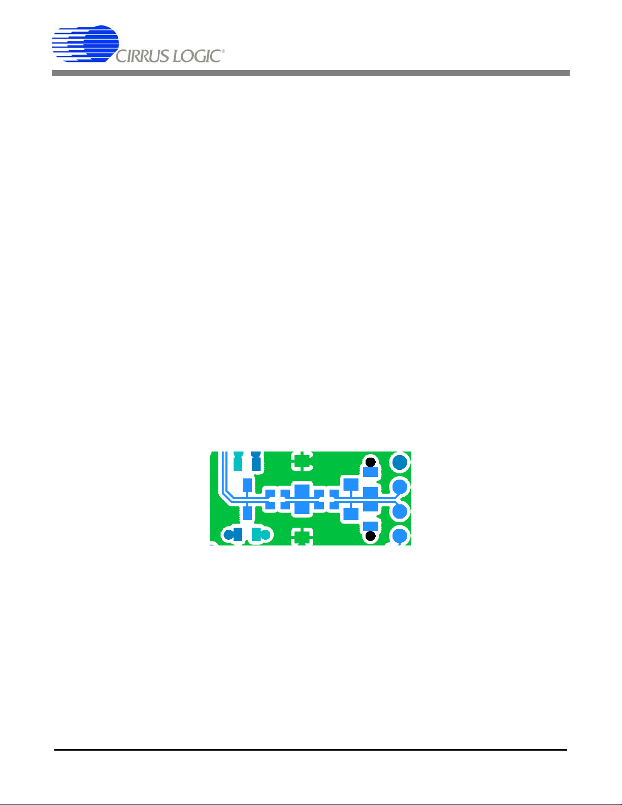
Figure 7. Dual-row Headers with Shorts
The dual-row header pins are shorted on the bottom side of the PCB to pass signals through to the rest
of the board. These shorted traces between the dual-row pins can be carefully
signals from the rest of the PCB to permit wiring changes to the existing route. To restore the previous
connection, install a jumper to short across the dual-row pins.
Signals taken off the PCB should not be wired directly from the dual-row header pins, as there is no clean
path for the signal return current. Instead, install a connector into the prototyping area and wire the signal
and a ground connection to it. Pairing the signal with a ground return before taking it off the PCB will improve signal integrity.
cut to isolate the device
34 DS862DB1
Page 35
CDB5374
3. SOFTWARE DESCRIPTION
3.1 Menu Bar
The menu bar is always present at the top of the software panels and provides typical File and Help pulldown menus. The menu bar also selects the currently displayed panel.
Control Description
File
Load Data Set Loads a data set from disk.
Save Data Set Saves the current data set to disk.
Copy Panel to Clipboard Copies a bitmap of the current panel to the clipboard.
Print Analysis Screen Prints the full Analysis panel, including statistics fields.
Print Analysis Graph Prints only the graph from the Analysis panel.
High Resolution Printing Prints using the higher resolution of the printer.
Low Resolution Printing Prints using the standard resolution of the screen.
Quit Exits the application software.
Setup! Displays the Setup Panel.
Analysis! Displays the Analysis Panel.
Control! Displays the Control Panel.
DataCapture! Displays the Setup Panel and starts Data Capture.
Help
Contents Find help by topic.
Search for help on Find help by keywords.
About Displays the About Panel.
DS862DB1 35
Page 36

3.2 About Panel
CDB5374
The About panel displays copyright information for the Cirrus Seismic Evaluation software.
Ö
Click OK to exit this panel. Select Help
36 DS862DB1
About from the menu bar to display this panel.
Page 37

3.3 Setup Panel
CDB5374
The Setup panel initializes the evaluation system to perform data acquisition. It consists of the following
sub-panels and controls.
• USB Port
• Digital Filter
• Analog Front End
• Test Bit Stream
• Gain/Offset
• Data Capture
• External Macros
DS862DB1 37
Page 38

CDB5374
3.3.1 USB Port
The USB Port sub-panel sets up the USB communication interface between the PC and the target board.
Control Description
Open Target Open USB communication to the target board and read the board name and micro-
controller firmware version. When communication is established, the name of this
control changes to ‘Close Target’ and Setup, Analysis and Control panel access
becomes available in the menu bar.
Close Target Disconnects the previously established USB connection. On disconnection, this con-
trol changes to ‘Open Target’ and the Setup, Analysis and Control panel access
becomes unavailable in the menu bar. The evaluation software constantly monitors
the USB connection status and automatically disconnect s if the target board is turned
off or the USB cable is unplugged.
Board Name Displays the type of target board currently connected.
MCU code version Displays the version number of the microcontroller code on the connected target
board.
Reset Target Sends a software reset command to the microcontroller.
Flash MCU Programs the microcontroller code on the target board using the .thx file found in the
“C:\Program Files\Cirrus Seismic Evaluation” directory. T his fe at ur e pe rm its reprogramming of the microcontroller (without using a hardware programmer ) when a new
version of the MCU code becomes available.
38 DS862DB1
Page 39

CDB5374
3.3.2 Digital Filter
The Digital Filter sub-panel sets up the digital filter configuration options.
By default the Digital Filter sub-panel configures the system to use on-chip coefficients and test bit
stream data. The on-chip data can be overwritten by loading custom coefficients and test bit stream da ta
from the Customize sub-panel on the Control panel.
Any changes made under this sub-panel will not be applied to the target board until the Configure button
is pushed. The Configure button writes the new configuration to the target board and then enables the
data Capture button.
Control Description
Channel Set Selects the number of channels that are enabl ed in the digit al filter. For the CS5376A
digital filter, from 1 to 4 channels can be enabled.
Output Rate Selects the output word rate of the digital filter. Output word rates from 4000 SPS to
1 SPS (0.25 mS to 1 S) are available.
Output Filter Selects the output filter stage from the digital filter. Sinc output, FIR1 output, FIR2
output, IIR 1st order output, IIR 2nd order output, or IIR 3rd order output can be
selected. FIR2 output provides full decimation of the modulator data.
FIR Coeff Selects the on-chip FIR coefficient set to use in the digital filter. Linear phase or mini-
mum phase FIR coefficients can be selected.
IIR Coeff Selects the on-chip IIR coefficient set to use in the digital filter. Coefficient sets pro-
ducing a 3 Hz high-pass corner at 2000 SPS, 1000 SPS, 500 SPS, 333 SPS, and
250 SPS can be selected.
Filter Clock Sets the digital filter internal clock rate. Lower internal clock rates can save power
when using slow output word rates.
MCLK Rate Sets the analog sample clock rate. The CS5374 modulators and CS4373A test DAC
typically run with MCLK set to 2.048 MHz.
Configure Writes all information from the Setup panel to the digital filter. The data Capture but-
ton becomes available once the configuration information is written to the target
board.
DS862DB1 39
Page 40

CDB5374
3.3.3 Analog Front End
The Analog Front End sub-panel configures the amplifier, modulator, and test DAC pin options. Pin options are controlled through the GPIO outputs of the digital filter.
Any changes made under this sub-panel will not be applied to the target board until the Configure button
is pushed. The Configure button writes the new configuration to the target board and then enables the
data Capture button.
Control Description
Amp Mux Selects the input source for the CS5374 amplifiers. An internal termination, external
INA inputs or external INB inputs can be selected.
DAC Mode Selects the operational mode of the CS4373A test DAC. The test DAC operational
modes are AC dual output (OUT&BUF), AC precision output (OUT only), AC buffered
output (BUF only), DC common mode output (DC Common), DC differential output
(DC Diff), or AC common mode output (AC Common). The test DAC can also be
powered down (PWDN) when not in use to save power.
Gain Sets the amplifier gain range and test DAC attenuation. Amplifier gain and DAC
attenuation settings of 1x, 2x, 4x, 8x, 16x, 32x, or 64x can be selected and are controlled together.
Sw Disabled for CDB5374.
3.3.4 Test Bit Stream
The Test Bit Stream sub-panel configures test bit stream (TBS) generator parameters. The digital filter
data sheet describes TBS operation and options.
The DAC Quick Set controls automatically set the Interpolation, Clock Rate, and Gain Factor controls
based on the selected Mode, Freq, and Gain. Additional configurations can be programmed by writing the
Interpolation, Clock Rate, and Gain Factor controls manually.
Any changes made under this sub-panel will not be applied to the target board until the Configure button
is pushed. The Configure button writes the new configuration to the target board and then enables the
data Capture button.
Control Description
DAC Quick Set Automatically set s test bit stream options. Mode select s sine or impulse output mo de,
Freq selects the test signal frequency for sine mode, an d Gain se lec t s the test sig nal
amplitude in dB.
Interpolation Manual control for the data interpolation factor of the test bit stream generator.
Clock Rate Manual control for the output clock and data rate of the test bit stream generator.
Gain Factor Manual control to set the test bit stream signal amplitude.
Sync Enables test bit stream synchronization by the MSYNC signal.
Loopback Enables digital loopback from the test bit stream generator output to the digital filter
input.
40 DS862DB1
Page 41

CDB5374
3.3.5 Gain/Offset
The Gain / Offset sub-panel controls the digital filter GAIN and OFFSET registers for each channel.
The OFFSET and GAIN registers can be manually written with any 24-bit 2’s complement value from
0x800000 to 0x7FFFFF. The USEGR, USEOR, ORCAL, and EXP[4:0] values enable gain correction, offset correction, and offset calibration in the digital filter.
The offset calibration routine built into the digital filter is enabled by writing the ORCAL and EXP[4:0] bits.
The EXP[4:0] value can range from 0x00 to 0x18 and represents an exponential shift of the calibration
feedback, as described in the digital filter data sheet. Offset calibration results are automatically written to
the OFFSET registers and remain there, even after offset calibration is disabled.
Control Description
Gain Displays the digital filter GAIN1 to GAIN4 registers.
Offset Displays the digital filter OFFSET1 to OFFSET4 registers.
Read Reads values from the GAIN and OFFSET registers.
Write Writes values to the GAIN and OFFSET registers.
USEGR Enables gain correction. When enabled, output samples are gained down by the
value in the GAIN register.(Output = GAIN / 0x7FFFFF).
USEOR Enables offset correction. When enabled, output samples are offset by the value in
the OFFSET register. (Output = Sample - OFFSET).
ORCAL Enables offset calibration using the exponent value from the EXP[4:0] control.
Results are automatically written to the OFFSET registers as they are calculated.
EXP[4:0] Sets the exponential value used by offset calibration.
DS862DB1 41
Page 42

CDB5374
3.3.6 Data Capture
The Data Capture sub-panel collects samples from the target board and sets analysis parameters.
When the Capture button is pressed, the requested number of samples are collected from the target board
through the USB port and are split among the enabled channels. A four-channel system, for example, will
collect (Total Samples / 4) samples per channel. The maximum number of samples that can be collected
is 1,048,576 (1M). The number of samples per channel should be a power of two for the analysis FFT
routines to work properly.
After data is collected, analysis is performed using the selected parameters and the re sults are disp layed
on the Analysis panel. The selected analysis window, bandwidt h limit, full scale code, and full scale volt-
age parameters can be modified for the data set currently in memory and the analysis re-run by pressing
the REFRESH button on the Analysis Panel.
Control Description
Total Samples Sets the total number of samples to be collected. Multichannel acquisitions split the
requested number of samples among the channels. A maximum of 1,048,576 (1M)
samples can be collected.
Window Selects the type of analysis windowing function to be applied to the collected data
set. Used to ensure proper analysis of discontinuous data sets.
Bandwidth Limit (Hz) Sets the frequency range over which to perform analysis, used to exclude higher-fre-
quency components. Default value of zero performs analysis for the full Nyquist frequency range.
Full Scale Code Defines the maximum positive full-scale 24-bit code from the digital filter. Used during
FFT noise analysis to set the 0 dB reference level.
Full Scale Voltage Defines the maximum peak-to-peak input voltage for the nV/√Hz
sis.
Total Captures Sets the number of data sets to be collected and averaged together in the FFT mag-
nitude domain. The maximum number of data sets that can be averaged is 100.
Capture Starts data collection from the target board through the USB port. After data collec-
tion, analysis is run using parameters from this sub-panel.
Remaining Captures Indicates how many more data captures are remaining to complete the requested
number of Total Captures. A zero value means that the current data capture is the
last one.
Skip Samples Sets the total number of samples to be skip pe d pr ior to data collection. A maximum
of 64K samples can be skipped
Spot Noise analy-
42 DS862DB1
Page 43

CDB5374
3.3.7 External Macros
Macros are generated within the Macros sub-panel on the Control panel. Once a macro has been built
it can either be saved with a unique macro name to be run within the Macros sub-panel, or saved as an
external macro and be associated with one of the External Macro buttons.
A macro is saved as an External Macro by saving it in the . /macros/ subdirectory using the name
‘m1.mac’, ‘m2.mac’, etc. Depending on the selected name the macro will be associated with the corresponding External Macro button M1, M2, etc.
• M1 = . /macros/m1.mac
• M2 = . /macros/m2.mac
•etc.
External Macro buttons can be re-named on the panel by right clicking on them. The button name will
change, but the macro associated with that button is always saved as ‘m1.mac’, ‘m2.mac’, etc., in the
./macros/ subdirectory. The External Macro button names are stored in the file ‘Mnames.txt’, also in the
./macros/ subdirectory.
External Macros allow up to eight macros to be accessed quickly without having to load them into the Mac-
ros sub-panel on the Control panel. These External Macros operate independently of the Macros subpanel and are not affected by operations within it, except when a macro is saved to the ./macros/ subdi-
rectory to replace a currently existing External Macro.
Control Description
M1 - M8 Runs the External Macro associated with that button.
DS862DB1 43
Page 44

3.4 Analysis Panel
CDB5374
The Analysis panel is used to display the analysis results on collected data. It consists of the following
controls.
• Test Select
• Statistics
• Plot Enable
• Cursor
• Zoom
• Refresh
• Harmonics
• Spot Noise
• Plot Error
44 DS862DB1
Page 45

CDB5374
3.4.1 Test Select
The Test Select control sets the type of analysis to be run on the collected data set.
Control Description
Time Domain Runs a min / max calculation on the collected data set and then plots sample data
value vs. sample number.
Histogram Runs a histogram calculation on the collected data set and then plots sample occur-
rence vs. sample value. Only valid for noise data since sine wave data varies over
too many codes to plot as a histogram.
Signal FFT Runs an FFT on the collected data set and then plots frequency magnitude vs. fre-
quency . Statistics are calculated using the largest frequency bin as a full-scale signal
reference.
Noise FFT Runs an FFT on the collected data set and then plots frequency magnitude vs. fre-
quency . Statistics are calculated using a simulated full-scale signal as a full-scale signal reference.
DS862DB1 45
Page 46

CDB5374
3.4.2 Statistics
The Statistics control displays calculated statistics for the selected analysis channel. For multichannel
data captures, only one channel of calculated statistics are displayed at a time and is selected using the
Statistics channel control.
Errors that affect statistical calculations will cause the Plot Error control to appear. Information about errors on specific channels can be accessed by enabling the plot of the channel using t he Plot Enable control and then accessing the Plot Error controls.
Control Description
Time Domain
Max Maximum code of collected data set.
Min Minimum code of collected data set.
Histogram
Max Maximum code of collected data set.
Min Minimum code of collected data set.
Mean Mean of collected data set.
Std D ev Standard Deviation of collected data set.
Variance Variance of collected data set.
Signal FFT
S/N Signal to Noise of calculated FFT.
S/PN Signal to Peak Noise of calculated FFT.
S/D Signal to Distortion of calculated FFT.
S/N+D Signal to Noise plus Distortion of calculated FFT.
# of bins Number of Bins covering the Nyquist frequency.
Noise FFT
S/N Signal to Noise of calculated FFT.
S/PN Signal to Peak Noise of calculated FFT.
Spot Noise dB Spot Noise in dB/Hz of calculated FFT.
Spot Noise nV Spot Noise in nV/√Hz
# of bins Number of Bins covering the Nyquist frequency.
of calculated FFT.
3.4.3 Plot Enable
The Plot Enable control selects which ch annels are plotted for the current analysis. Multichannel plots are
overlay plots with the highest number channel displayed as the top most plot. Only channels enabled by
the Plot Enable control will report analysis error codes. Information about error codes can be accessed
through the Plot Error controls.
46 DS862DB1
Page 47

CDB5374
3.4.4 Cursor
The Cursor control is used to identify a point on the graph using the mouse and then display its plot values.
When any point within the plot area of the graph is clicked, the Cursor will snap to the closest plotted point
and the plot values for that point display below the graph.
When using the Zoom function, the Cursor is used to select the corners of the area to zoom.
3.4.5 Zoom
The ZOOM function allows an area on the graph to be expanded. To use the zoom function, click the
ZOOM button and select the box corners of the area on the graph to expand. The graph will then e xpand
to show the details of this area, and the plot axes will be re-scaled. While zoomed, you can zoom in farther
by repeating the process.
To restore the graph to its original scale, click the RESTORE button that appears while zoomed. If multiple
zooms have been initiated, the RESTORE button will return to the previo usly viewed plot scale. Repeated
RESTORE will eventually return to the original plot scale. From within multiple zooms the original scale
can be directly restored by clicking the REFRESH button.
3.4.6 Refresh
The REFRESH button will clear and re-plot the current data set. Refresh can be used to apply new anal-
ysis parameters from the Data Capture sub-panel, or to restore a ZOOM graph to its default plot scale.
3.4.7 Harmonics
The HARMONICS control is only visible during a Signal FFT analysis and highligh ts the fundamental and
harmonic bins used to calculate the Signal FFT statistics. HARMONICS highlighting helps to understand
the source of any Signal FFT plot errors.
3.4.8 Spot Noise
The Spot Noise control (lab eled dB or nV) is only visible during a Noise FFT analysis a nd selects the units
used for plotting the graph, either dB/Hz or nV/√Hz
the Data Capture sub-panel on the Setup panel to determine the 0 dB point of the dB axis. The nV/√Hz
plot applies the Full Scale Voltage value from the Data Capture sub-panel on the Setup panel to determine the absolute scaling of the nV axis.
. The dB/Hz plot applies the Full Scale Code value from
3.4.9 Plot Error
The PLOT ERROR control provides information about errors that occurred during an analysis. Analysis
errors are only reported if the channel that has the error is currently plotted.
An analysis error stores an error code in the numerical display box of the PLOT ERROR control. If more
than one error occurs, all error codes are stored and the last error code is displayed. Any o f the accumulated error codes can be displayed by clicking on the numerical box and selecting it.
Once an error code is displayed in the numerical box, a description can be displayed by clicking the PLOT
ERROR button. This causes a dialog box to display showing the error number, the error channel, and a
text error message.
DS862DB1 47
Page 48
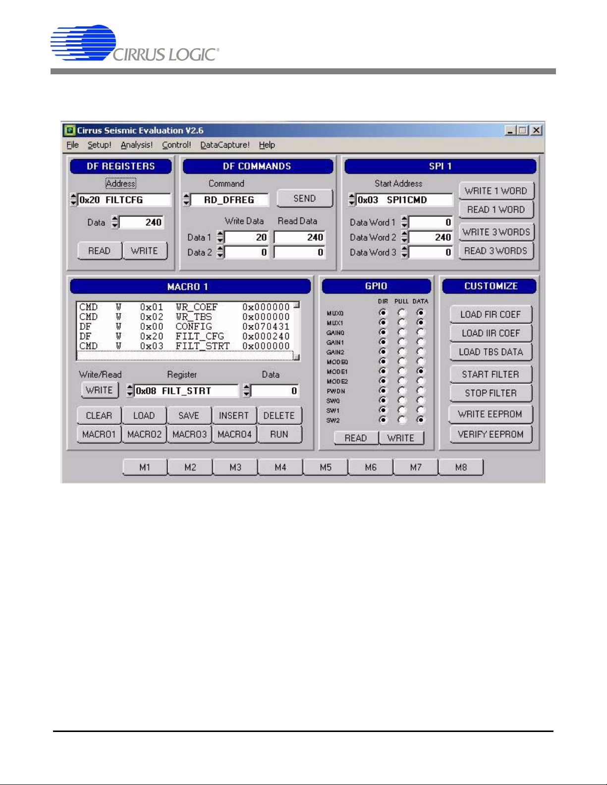
3.5 Control Panel
CDB5374
The Control panel is used to write and read register settings and to send commands to the digital filter.
It consists of the following sub-panels and controls.
• DF Registers
• DF Commands
• SPI1
• Macros
•GPIO
• Customize
• External Macros
48 DS862DB1
Page 49

CDB5374
3.5.1 DF Registers
The DF Registers sub-panel writes and reads registers within the digital filter. Digital filter registers control operation of the digital filter and the included hardware peripherals, as described in the digital filter
data sheet.
Control Description
Address Selects a digital filter register.
Data Contains the data written to or read from the register.
Read Initiates a register read.
Write Initiates a register write.
3.5.2 DF Commands
The DF Commands sub-panel sends commands to the digital filter. The digital filter commands and their
required parameters are described in the digital filter data sheet.
Not all commands require write data values, and not all commands will return read data values. Some
commands require formatted data files for uploading custom coefficients or test bit stream data example
formatted data files are included in the SPI sub-directory of the software installation.
Control Description
Command Selects the command to be written to the digital filter.
Write Data 1 Contains the SPI1DAT1 data to be written to the digital filter.
Write Data 2 Contains the SPI1DAT2 data to be written to the digital filter.
Read Data 1 Contains the SPI1DAT1 data read from the digital filter.
Read Data 2 Contains the SPI1DAT2 data read from the digital filter.
Send Initiates the digital filter command.
3.5.3 SPI
The SPI sub-panel writes and reads registers in the digital filter SPI register space. They can be used to
check the SPI serial port status bits or to manually write commands to the digital filter.
Control Description
Start Address Selects the address to begin the SPI transaction.
Data Word 1 Contains the first data word written to or read from the SPI registers.
Data Word 2 Contains the second data word written to or read from the SPI registers.
Data Word 3 Contains the third data word written to or read from the SPI registers.
Read 1 Word Initiates a 1 word SPI read transaction.
Read 3 Words Initiates a 3 word SPI read transaction.
Write 1 Word Initiates a 1 word SPI write transaction.
Write 3 Words Initiates a 3 word SPI write transaction.
DS862DB1 49
Page 50

CDB5374
3.5.4 Macros
The Macros sub-panel is designed to write a large number of registers with a single command. This allows the target evaluation system to be quickly set into a specific state for testing.
The Register control gives access to both digital filter registers and SPI1 registers. These registers can
be written with data from the Data control, or data can be read and output to a text window. The Register
control can also select special commands to be executed, with the Data control used to define a parameter value for the special command, if necessary.
Control Description
Write / Read Selects the type of operation to be performed by the inserted macro command.
Register Selects the target register for the inserted macro command. Also selects special
commands that can be performed.
Data Sets the register data value for the inserted macro command. Also sets the parame-
ter value for special commands.
Clear Clears the currently displayed macro.
Load Loads a previously saved macro.
Save Saves the currently displayed macro. Macros can be saved with unique names or
can be saved as External Macros.
Insert Inserts a macro command at the selected macro line. The macro command is built
from the Write/Read, Register, and Data controls.
Delete Deletes the macro command at the selected macro line.
Macro1 - Macro4 Selects which of the four working macros is displayed.
Run Runs the currently displayed working macro.
3.5.5 GPIO
The GPIO sub-panel controls the digital filter GPIO pin configurations. GPIO pins have dedicated functions on the target board, but can be used in any manner for custom designs.
Control Description
Direction Sets the selected GPIO pin as an output (*) or input ( ).
Pull Up Turns the pull up resistor for the selected GPIO pin on (*) or off ( ).
Data Sets the selected output GPIO pin to a high (*) or low ( ) level.
Write Initiates a write to GPIO registers.The Direction, Pull Up and Data controls are read
to determine the register values to be written.
Read Initiates a read from GPIO registers.The Direction, Pull Up and Data controls are
updated based on the register values that are read.
50 DS862DB1
Page 51

CDB5374
3.5.6 Customize
The Customize sub-panel sends commands to upload custom FIR and IIR filter coefficients, upload custom test bit stream data, start the digital filter, stop the digital filter, and write/read custom EEPROM configuration files to the on-board boot EEPROM. Example data files are included in a sub-directory of the
software installation.
Control Description
Load FIR Coef Write a set of FIR coefficients into the digital filter from a file.
Load IIR Coef Write a set of IIR coefficients into the digital filter from a file.
Load TBS Data Write a set of test bit stream data into the digital filter from a file.
Start Filter Enables the digital filter by sending the Start Filter command.
Stop Filter Disables the digital filter by sending the Stop Filter command.
Write EEPROM Writes an EEPROM boot configuration file to the EEPROM memory.
Verify EEPROM Verifies EEPROM memory against an EEPROM boot configuration file.
3.5.7 External Macros
Macros are generated within the Macros sub-panel on the Control panel. Once a macro has been built
it can either be saved with a unique macro name to be run within the Macros sub-panel, or saved as an
external macro and be associated with one of the External Macro buttons.
A macro is saved as an External Macro by saving it in the ./macros/ subdirectory using the name
‘m1.mac’, ‘m2.mac’, etc. Depending on the selected name the macro will be associated with the corresponding External Macro button M1, M2, etc.
• M1 = . /macros/m1.mac
• M2 = . /macros/m2.mac
•etc.
External Macro buttons can be re-named on the panel by right clicking on them. The button name will
change, but the macro associated with that button is always saved as ‘m1.mac’, ‘m2.mac’, etc., in the
./macros/ subdirectory. The External Macro button names are stored in the file ‘Mnames.txt’, also in the
./macros/ subdirectory.
External Macros allow up to eight macros to be accessed quickly without having to load them into the Mac-
ros sub-panel on the Control panel. These External Macros operate independently of the Macros subpanel and are not affected by operations within it, except when a macro is saved to the ./macros/ subdi-
rectory to replace a currently existing External Macro.
Control Description
M1 - M8 Runs the External Macro associated with that button.
DS862DB1 51
Page 52
4. BILL OF MATERIALS
KEMET C0805C104K5RAC
KEMET C1206C103J3GAC
NO POP NP-CAP-1206 DO NOT POPULATE
ON SEMICONDUCTOR BAV99LT1G
WIRE. L 1.500 X 0.250T X 0.250T
TYPE E 24/19 BLU SQUIRES ELEC.
WIRE. L 1.500 X 0.250T X 0.250T
WIRE. L 1.500 X 0.250T X 0.250T
108-0904-001 REQUIRES BINDING POST HOOK UP
COMPONENTS
TYPE E 24/19 BLU SQUIRES ELEC.
TYPE E 24/19 BLU SQUIRES ELEC.
INC.
108-0907-001 REQUIRES BINDING POST HOOK UP
COMPONENTS
INC.
INC.
108-0903-001 REQUIRES BINDING POST HOOK UP
108-0902-001 REQUIRES BINDING POST HOOK UP
COMPONENTS
WIRE. L 1.500 X 0.250T X 0.250T
TYPE E 24/19 BLU SQUIRES ELEC.
INC.
SAMTEC TSW-102-07-G-D
COMPONENTS
CDB5374
TP-101-10
ED 100/2DS
CORPORATION
TECHNOLOGY
DALE CRCW060310R0FKEA
BILL OF MATERIAL (Page 1 of 2)
C27 C30 C31 C32 C33 C34 C36 C37 C38 C39
C40 C41 C43 C44 C48 C49 C51 C52 C54 C55
C57 C60 C61 C62 C66 C67 C68 C69 C71 C72
C73 C74 C75 C76 C77 C78 C79 C80 C81 C82
C83 C88 C89 C90 C98 C99 C100 C101 C506
C509 C513 C516
Item Cirrus P/N Rev Description Qty Reference Designator MFG MFG P/N Notes
CIRRUS LOGIC
CDB5374-Z_Rev_A.bom
1 001-04345-Z1 A CAP 0.1uF ±10% 50V X7R NPb 0805 63 C1 C2 C11 C12 C13 C15 C16 C17 C24 C25 C26
2 001-04076-Z1 A CAP 0.01uF ±10% 50V NPb X7R 0805 8 C3 C4 C5 C9 C10 C14 C22 C23 KEMET C0805C103K5RAC
C91 C92 C93 C94 C95 C96 C97 C507 C510
C258 C346 C350 C353 C356 C358 C446 C450
C453 C456 C458
D307 D308 D405 D406 D407 D408
3 004-00102-Z1 A CAP 100uF ±10% 16V TANT NPb CASE D 11 C6 C7 C8 C18 C19 C20 C21 C28 C29 C35 C520 KEMET T491D107K016AT
4 001-06603-Z1 A CAP 0.01uF ±5% 25V C0G NPb 1206 19 C42 C45 C63 C64 C65 C70 C84 C85 C86 C87
5 000-00009-Z1 A NO POP CAP NPb 1206 0 C46 C50 C53 C56 C58 C246 C250 C253 C256
6 004-00068-Z1 A CAP 4.7uF ±10% 10V NPb TANT CASE A 1 C59 KEMET T491A475K010AT
7 070-00004-Z1 A DIODE SCHTTKY BARR 30V 0.2A NPb AXL 4 D1 D2 D3 D4 PHILIPS BAT85
8 070-00024-Z1 A DIODE SWT 70V 215mA NPb SOT-23 16 D5 D6 D7 D8 D205 D206 D207 D208 D305 D306
9 070-00055-Z1 A DIODE ARRAY 5V (TVS) ESD NPb SOT143 1 D9 LITTELFUSE SP0503BAHTG
10 165-00004-Z1 A LED SUP RED 1.7V 1mA 1.6MCD NPb SMD 1 D10 CHICAGO MINIATURE CMD28-21SRC/TR8/T1
11 115-00061-Z1 A HDR 12x2 ML .1" CTR 062 S GLD NPb 0 J1 J5 J30 J36 J37 J42 J64 J65 SAMTEC TSW-112-07-G-D DO NOT POPULATE
12 110-00028-Z1 A CON BNC-PCB RCPT NPb RA 1 J4 KINGS KC-79-237 M06
13 130-00007-Z1 A JACK BAN SOLDR TERM NYL INS GRN NPb 1 J6 JOHNSON
14 130-00009-Z1 A JACK BAN SOLDR TERM NYL INS YLW NPb 1 J7 JOHNSON
15 130-00014-Z1 A JACK BAN SOLDR TERM NYL INS BLK NPb 1 J8 JOHNSON
16 130-00006-Z1 A JACK BAN SOLDR TERM NYN INS RED NPb 1 J9 JOHNSON
J66 J519
28 115-00014-Z1 A HDR 2x1 ML .1" 062BD ST GLD NPb TH 1 J56 SAMTEC TSW-102-07-G-S
17 115-00016-Z1 A HDR 3x2 ML .1"CTR 062 S GLD NPb 3 J10 J11 J21 SAMTEC TSW-103-07-G-D
18 115-00013-Z1 A HDR 2x2 ML .1"CTR .062BD S GLD NPb 13 J12 J13 J19 J20 J22 J23 J28 J33 J34 J43 J58
19 115-00012-Z1 A HDR 4x2 ML .1"CTR S GLD NPb 4 J14 J15 J24 J25 SAMTEC TSW-104-07-G-D
20 115-00030-Z1 A HDR 6x2 ML .1"CTR 062 S GLD NPb 1 J16 SAMTEC TSW-106-07-G-D
21 115-00029-Z1 A HDR 8x2 ML .1" 062BD ST GLD NPB TH 6 J17 J18 J27 J227 J327 J427 SAMTEC TSW-108-07-G-D
22 115-00011-Z1 A HDR 10x2 ML .1" 062BD ST GLD NPb TH 1 J26 SAMTEC TSW-110-07-G-D
23 115-00023-Z1 A HDR 14x2 ML .1"CTR 062 S GLD NPb 0 J29 J35 SAMTEC TSW-114-07-G-D DO NOT POPULATE
24 110-00055-Z1 A CON TERM BLCK 4 POS 5mm NPb BLU TH 8 J32 J41 J232 J241 J332 J341 J432 J441 OST ED 100/4DS
25 115-00176-Z1 A HDR 7x2 ML 2MM 062BD S GLD TH NPb 1 J39 MOLEX 87758-1416
26 110-00041-Z1 A CON RA USB BLK NPb TH 1 J47 AMP 292304-1
27 110-00056-Z1 A CON TERM BLOCK 2POS 5mm NPb BLU TH 3 J50 J59 J63 ON-SHORE
29 115-00003-Z1 A HDR 5x2 ML .1"CTR S GLD NPb 1 J60 SAMTEC TSW-105-07-G-D
R514 R519
33 020-01244-Z1 A RES 100k OHM 1/10W ±1% NPb 0603 7 R2 R42 R46 R53 R57 R59 R60 DALE CRCW0603100KFKEA
31 304-00001-Z1 A SPCR STANDOFF 4-40 THR .875L AL NPb 8 MH1 MH2 MH3 MH4 MH5 MH6 MH7 MH8 KEYSTONE 1809 REQUIRES 4-40- PAN HEAD SCREW
32 020-00788-Z1 A RES 10 OHM 1/10W ±1% NPb 0603 FILM 13 R1 R5 R11 R13 R14 R15 R16 R24 R25 R26 R68
30 080-00004-Z1 A WIRE JUMPER 2P 0.1" BRASS NPb TH 8 JP1 JP2 JP3 JP4 JP5 JP6 JP7 JP8 COMPONENTS
52 DS862DB1
Page 53

C8051F320-GQ PROGRAM AT TEST
CDB5374
DALE CRCW060310K0FKEA
NO POP NP-RES-0805 DO NOT POPULATE
BILL OF MATERIAL (Page 2 of 2)
R74 R75 R501 R511 R515
R352 R443 R452
DALE CRCW06030000ZSEA
DALE CRCW0603680RFKEA
R244 R245 R248 R249 R334 R336 R344 R345
R348 R349 R434 R436 R444 R445 R448 R449
R81 R82 R83 R84 R85 R86
BUILDING FASTENERS PMSSS 440 0031 PH SCREWS FOR STANDOFFS
LABORATORIES INC
XMH8
64 061-00061-Z1 A IC LOG 2IN XOR NPb SOT23-5 1 U505 TEXAS INSTRUMENTS SN74LVC1G86DBVR
65 060-00175-Z1 A IC 1.25MHz R2R OPAMP NPb SOT23-5 1 U507 LINEAR TECH LT1783IS5#TRMPBF
66 080-00003-Z1 A WIRE BPOST 1.5X.25 24/19 GA BLU NPb 4 XJ6 XJ7 XJ8 XJ9 SQUIRES L-1.5X.25TX.25T_TYPE_E_ WIRES FOR BINDING POSTS
67 300-00025-Z1 A SCREW 4-40X5/16" PH MACH SS NPb 8 XMH1 XMH2 XMH3 XMH4 XMH5 XMH6 XMH7
68 102-00017-Z1 A OSC 32.768MHz 50ppm 3.3V VCL NPb SM 1 Y1 CITIZEN CSX750VKB32.768M-UT
69 070-00005-Z1 A DIODE TR 13V 600W NPb AXL 3 Z1 Z2 Z3 LITTLE FUSE P6KE13A
70 240-00355-Z1 A PCB CDB5374 1 CIRRUS LOGIC 240-00355-Z1
71 603-00355-Z1 A ASSY DWG CDB5374 REF CIRRUS LOGIC 603-00355-Z1
72 600-00355-Z1 A SCHEM CDB5374 REF CIRRUS LOGIC 600-00355-Z1
73 115-00003-Z1 A HDR 5x2 ML .1"CTR S GLD NPb 0 J31 J40 J503 J525 J526 SAMTEC TSW-105-07-G-D DO NOT POPULATE
74 115-00029-Z1 A HDR 8x2 ML .1" 062BD ST GLD NPB TH 0 J38 J48 J49 J51 SAMTEC TSW-108-07-G-D DO NOT POPULATE
75 115-00011-Z1 A HDR 10x2 ML .1" 062BD ST GLD NPb TH 0 J44 J46 J52 J53 J54 J55 J61 J62 SAMTEC TSW-110-07-G-D DO NOT POPULATE
76 115-00012-Z1 A HDR 4x2 ML .1"CTR S GLD NPb 0 J45 SAMTEC TSW-104-07-G-D DO NOT POPULATE
77 115-00013-Z1 A HDR 2x2 ML .1"CTR .062BD S GLD NPb 0 J57 SAMTEC TSW-102-07-G-D DO NOT POPULATE
Item Cirrus P/N Rev Description Qty Reference Designator MFG MFG P/N Notes
34 020-00934-Z1 A RES 200 OHM 1/10W ±1% NPb 0603 FILM 10 R3 R17 R39 R40 R41 R55 R63 R69 R70 R71 DALE CRCW0603200RFKEA
CIRRUS LOGIC
CDB5374-Z_Rev_A.bom
35 020-01130-Z1 A RES 10k OHM 1/10W ±1% NPb 0603 FILM 16 R4 R6 R7 R8 R18 R20 R47 R51 R54 R56 R73
43 020-01048-Z1 A RES 2k OHM 1/10W ±1% NPb 0603 FILM 8 R35 R37 R235 R237 R335 R337 R435 R437 DALE CRCW06032K00FKEA
41 021-01391-Z1 A RES 18M OHM 1/8W ±5% NPb 0805 8 R31 R38 R231 R238 R331 R338 R431 R438 PANASONIC ERJ6GEYK186V
36 020-01074-Z1 A RES 3.32k OHM 1/10W ±1% NPb 0603 2 R9 R58 DALE CRCW06033K32FKEA
40 020-06288-Z1 A RES 680 OHM 1/10W ±1% NPb 0603 FILM 16 R27 R28 R29 R30 R72 R76 R77 R78 R79 R80
37 020-01128-Z1 A RES 9.53k OHM 1/10W ±1% NPb 0603 3 R10 R12 R21 DALE CRCW06039K53FKEA
38 020-01104-Z1 A RES 5.9k OHM 1/10W ±1% NPb 0603 FLM 1 R19 DALE CRCW06035K90FKEA
39 000-00001-Z1 A NO POP RES NPb 0805 0 R22 R23 R32 R33 R43 R52 R243 R252 R343
44 020-06253-Z1 A RES 412k OHM 1/4W ±1% NPb 1206 4 R50 R87 R88 R89 DALE CRCW1206412KFKEA
42 020-00673-Z1 A RES 0 OHM 1/10W ±5% NPb 0603 FILM 25 R34 R36 R44 R45 R48 R49 R62 R234 R236
45 000-00002-Z1 A NO POP RES NPb 0603 0 R61 NO POP NP-RES-0603 DO NOT POPULATE
46 020-01016-Z1 A RES 1k OHM 1/10W ±1% NPb 0603 FILM 4 R64 R65 R66 R67 DALE CRCW06031K00FKEA
47 120-00002-Z1 A SWT SPST 130G 0/1 5mm TACT ESD NPb 3 S2 S3 S4 C&K PTS645TL50 INSTALL AFTER WASH PROCESS
48 120-00011-Z1 A SWT 4 POS DIP RAISED NPb SPST 1 S5 GRAYHILL 76SB04T INSTALL AFTER WASH PROCESS
49 060-00195-Z1 A IC LOW V DUL SPST ANA SW NPb MSP8 2 U1 U2 VISHAY DG2003DQ-T1-E3 ALTERNATE is DG2037DQ-T1-E3
50 060-00063-Z1 A IC LNR V REG 200mA ADJ NPb SOT23-5 1 U3 LINEAR TECH LT1964ES5-BYP#PBF
51 061-00062-Z1 A IC LOG SGL D-FF CLR PREST NPb SSOP8 5 U4 U9 U10 U15 U16 TEXAS INSTRUMENTS SN74LVC2G74DCTRE4
52 060-00062-Z1 A IC LN V REG LNOIS 500mA NPb SO8-150 4 U5 U6 U7 U8 LINEAR TECH LT1763CS8#PBF
53 065-00178-Z1 E IC CRUS LOW V AMP DC-1kHz NPb SOIC8 1 U11 CIRRUS LOGIC CS3011-ISZ/E
54 060-00162-Z1 A IC 3.3V U LW PWR RS485 XCVR NPSOIC8 4 U12 U13 U17 U18 LINEAR TECH LTC1480IS8#PBF
55 060-00236-Z1 A IC LNR PRC VRF 2.5V TC10 NPbSO8-150 1 U14 LINEAR TECH LT1019AIS8-2.5#PBF ALTERNATE is LT1019IS8-2.5#PBF
56 065-00287-Z1 A0 IC CRUS DL HIPER AMP MOD NPb QFN48 2 U19 U21 CIRRUS LOGIC CS5374-INZ/A0
57 065-00173-Z1 D IC CRUS TEST DAC SSOP28 NPb 1 U20 CIRRUS LOGIC CS4373A-ISZ/D
58 065-00056-Z1 A IC CRUS LPWR MCH FLTR NPb TQFP64 1 U22 CIRRUS LOGIC CS5376A-IQZ/A
59 060-00067-Z1 A IC LNR DL CMOS SW DBNCR NPb SOT23-6 2 U23 U26 MAXIM MAX6817EUT+T
60 061-00064-Z1 A IC LOG, HEX INVERTER NPb SO14-150 1 U24 TEXAS INSTRUMENTS SN74LVC04ADE4
61 062-00022-Z1 A IC PGM EEPROM 8kX8 SPISER NPb SOIC8 1 U25 ATMEL AT25640AN-10SU-2.7
62 062-00055-Z1 A IC PGM 128 MCROCLL CPLD NPb VQFP100 1 U27 XILINX XCR3128XL-10VQG100I
63 062-00079-Z1 A IC PGM USB 16kB FLAS MCU NPb LQFP32 1 U28 SILICON
78 115-00030-Z1 A HDR 6x2 ML .1"CTR 062 S GLD NPb 0 J502 J541 J545 SAMTEC TSW-106-07-G-D DO NOT POPULATE
DS862DB1 53
Page 54

5. LAYER PLOTS
CDB5374
54 DS862DB1
Page 55
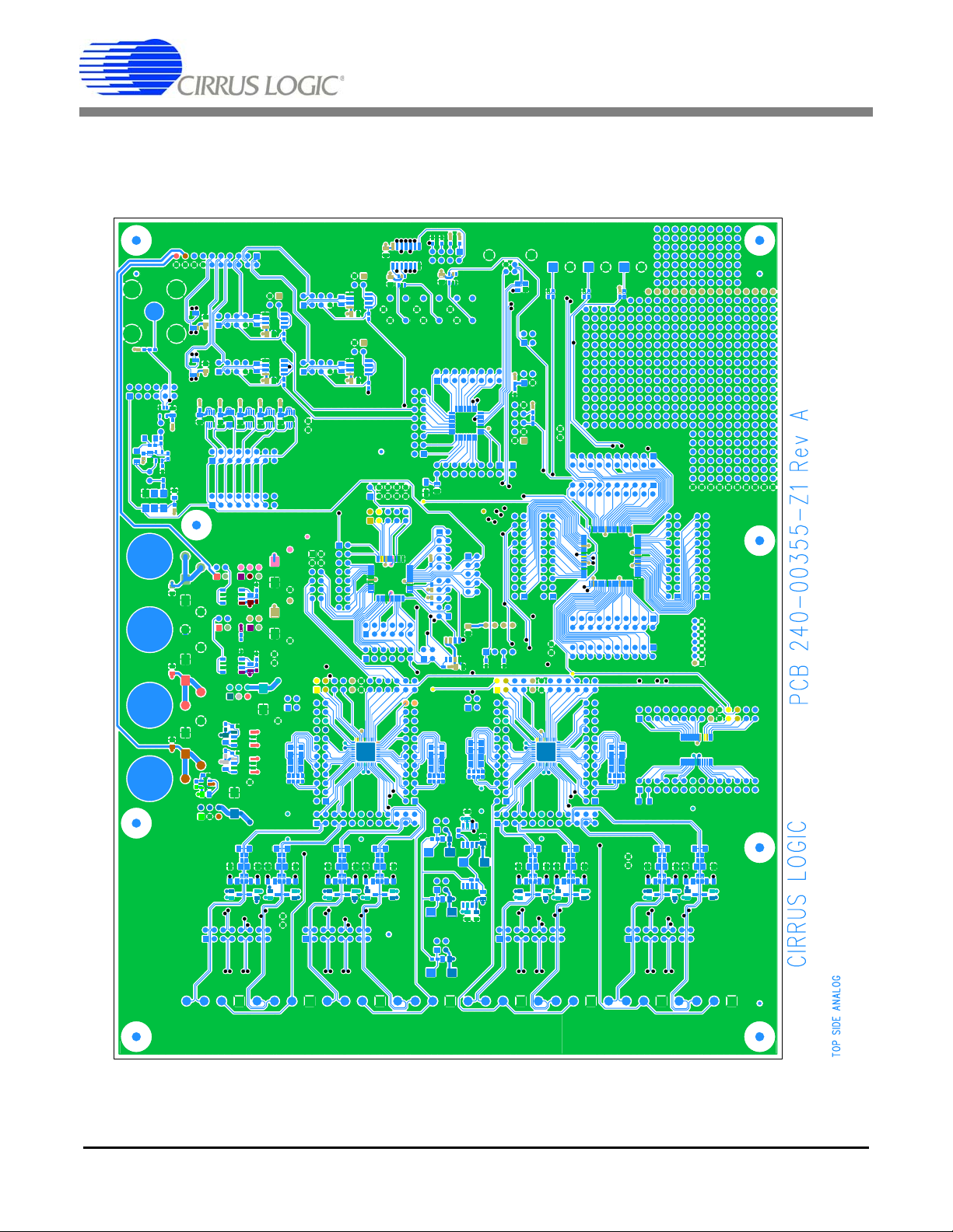
CDB5374
DS862DB1 55
Page 56

CDB5374
56 DS862DB1
Page 57

CDB5374
DS862DB1 57
Page 58
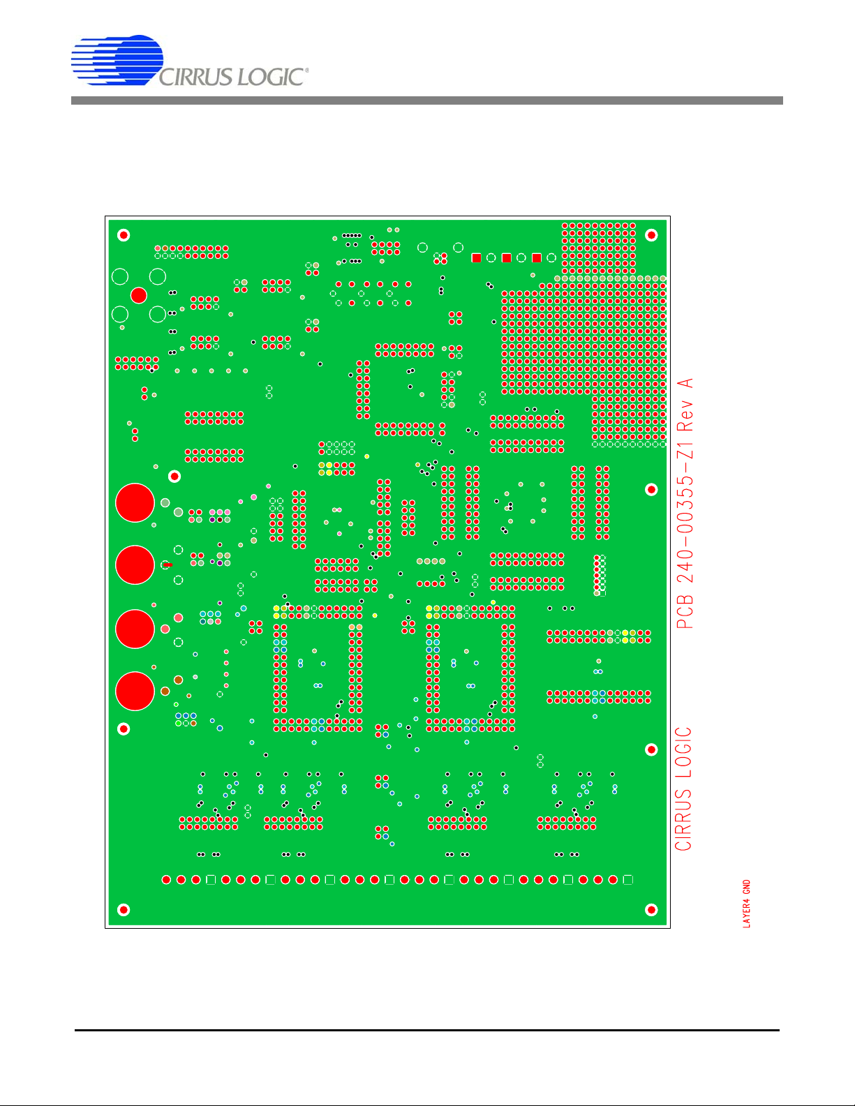
CDB5374
58 DS862DB1
Page 59
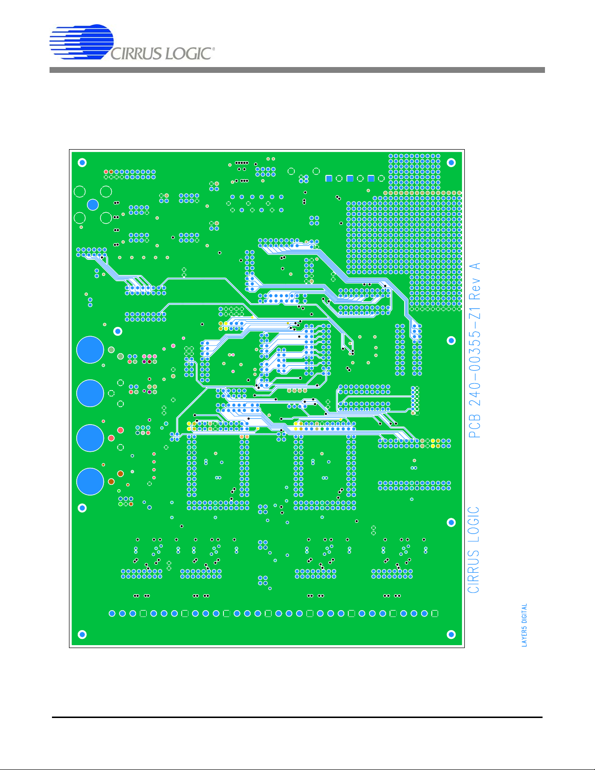
CDB5374
DS862DB1 59
Page 60

CDB5374
60 DS862DB1
Page 61

CDB5374
DS862DB1 61
Page 62
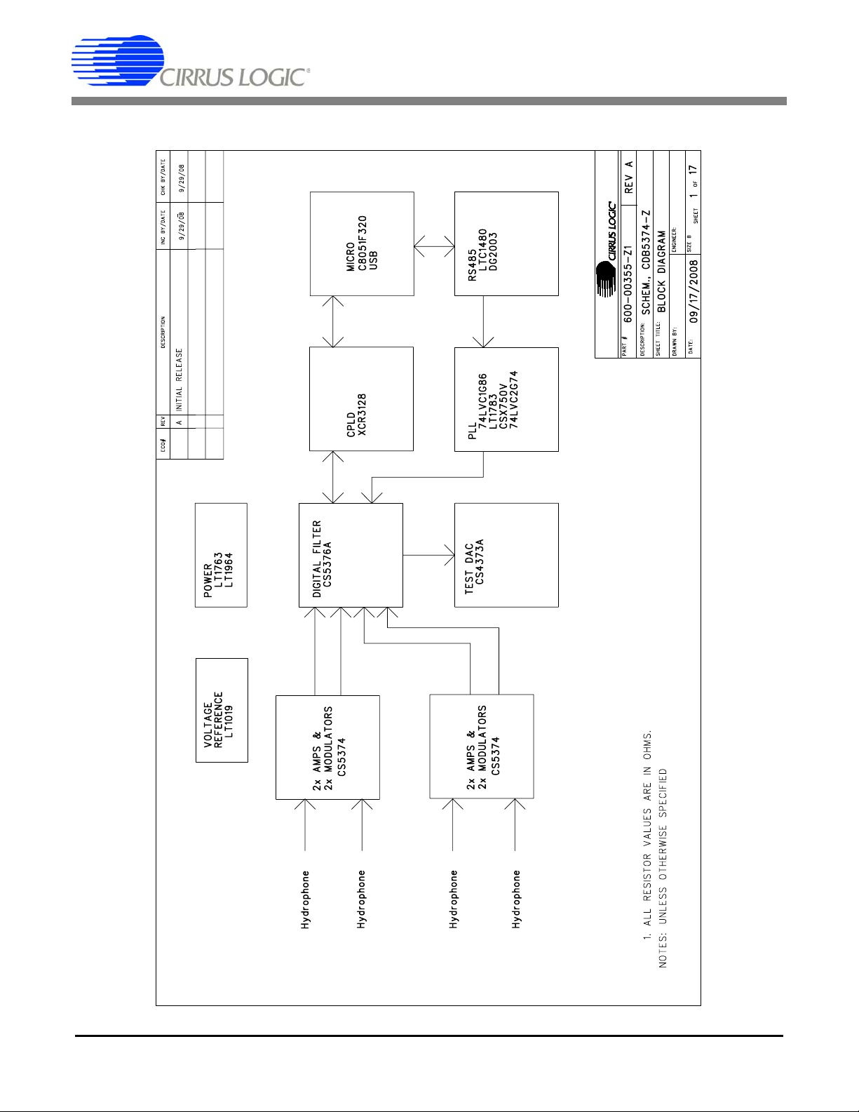
6. SCHEMATICS
CDB5374
62 DS862DB1
Page 63
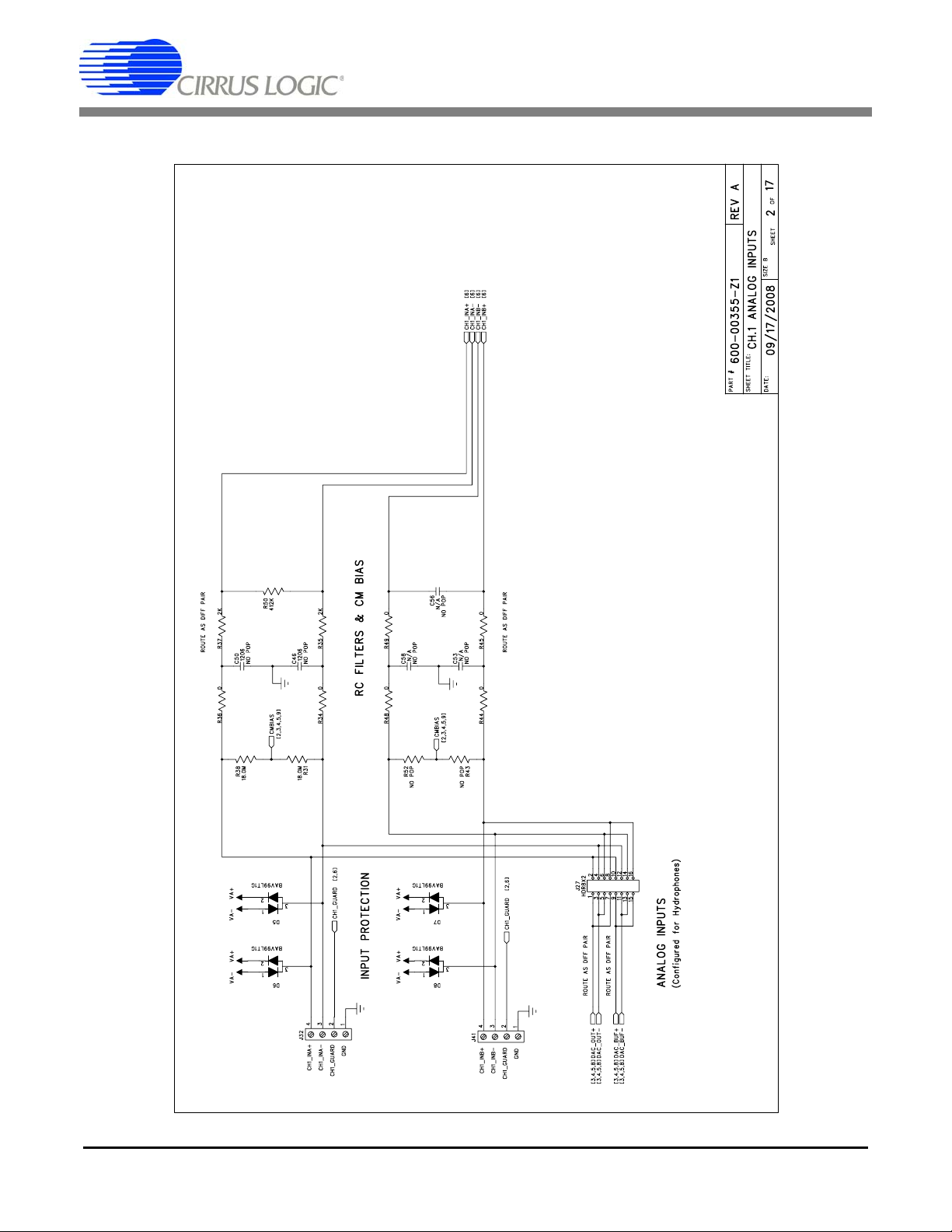
CDB5374
DS862DB1 63
Page 64

CDB5374
64 DS862DB1
Page 65

CDB5374
DS862DB1 65
Page 66
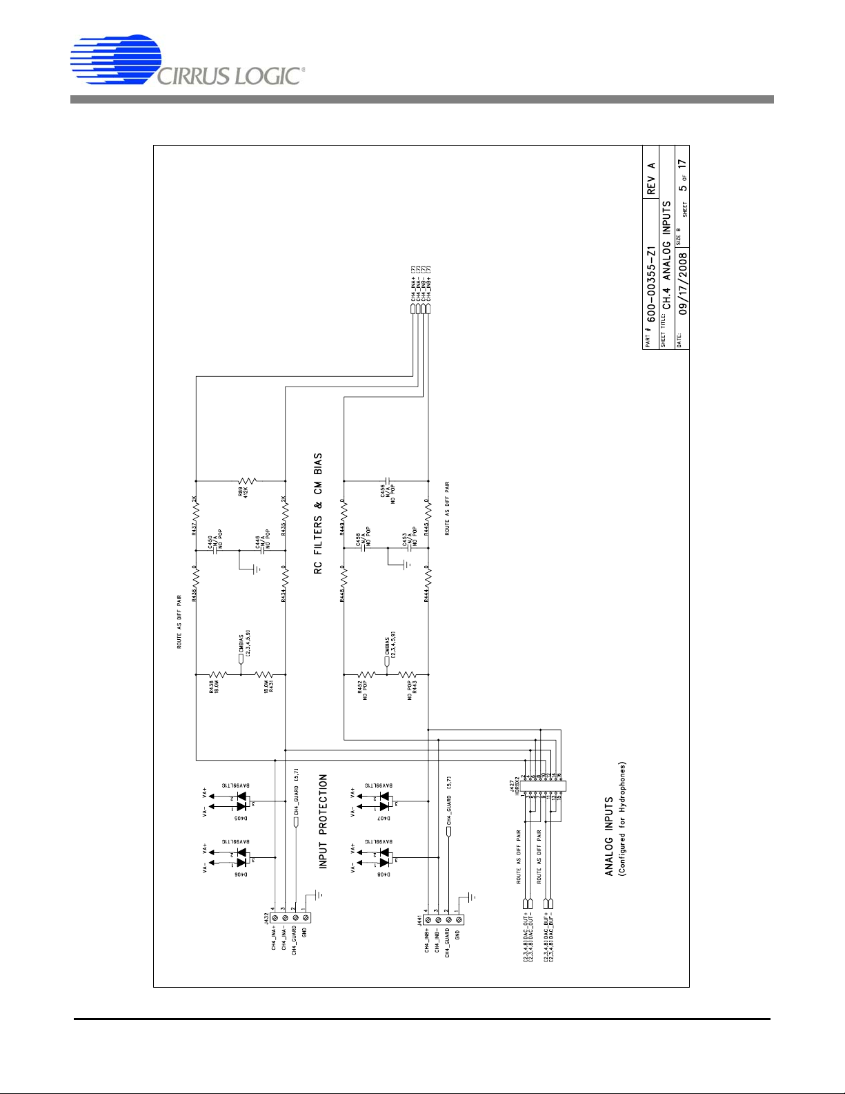
CDB5374
66 DS862DB1
Page 67
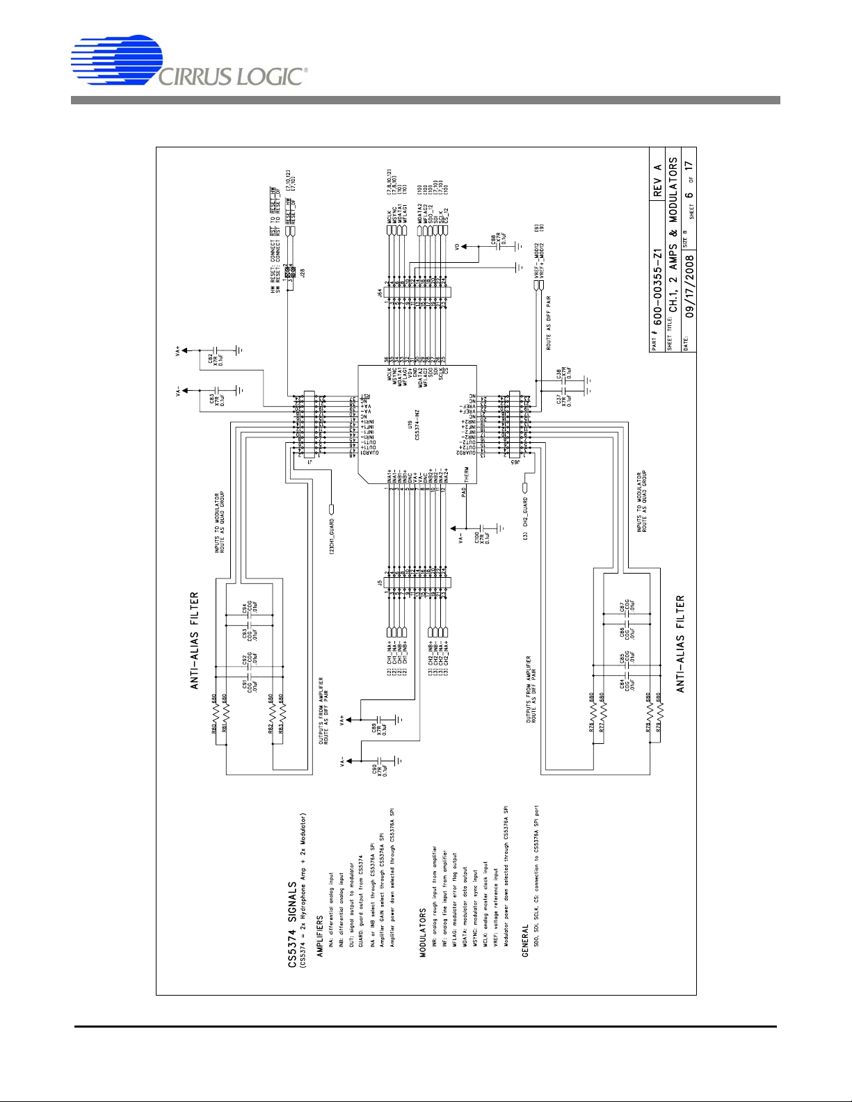
CDB5374
DS862DB1 67
Page 68

CDB5374
68 DS862DB1
Page 69

CDB5374
DS862DB1 69
Page 70
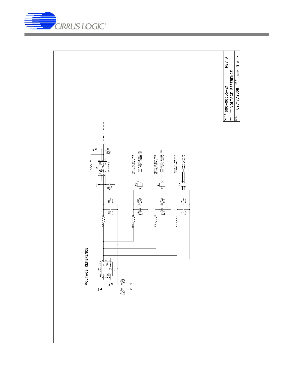
CDB5374
70 DS862DB1
Page 71

CDB5374
DS862DB1 71
Page 72

CDB5374
72 DS862DB1
Page 73

CDB5374
DS862DB1 73
Page 74
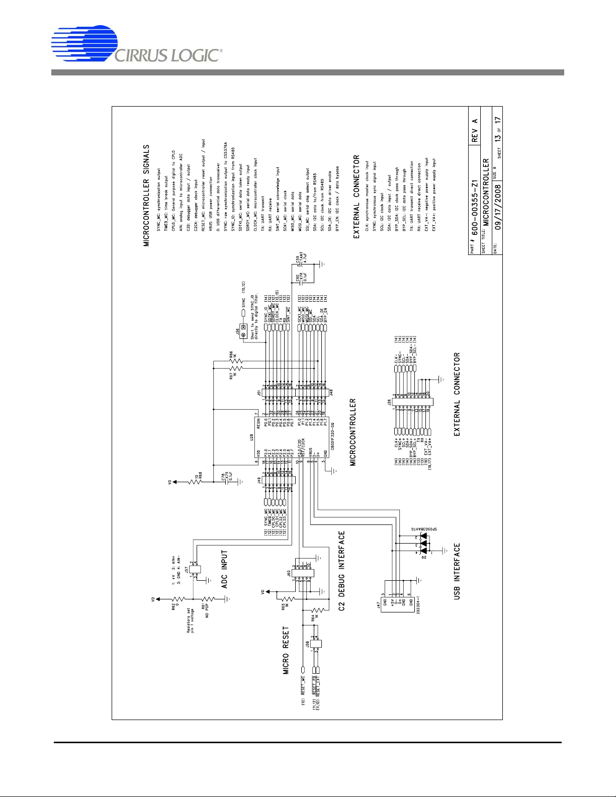
CDB5374
74 DS862DB1
Page 75
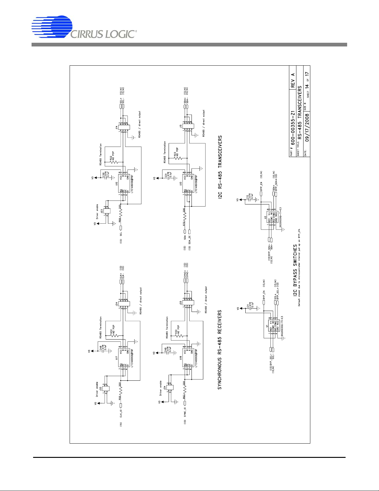
CDB5374
DS862DB1 75
Page 76

CDB5374
76 DS862DB1
Page 77
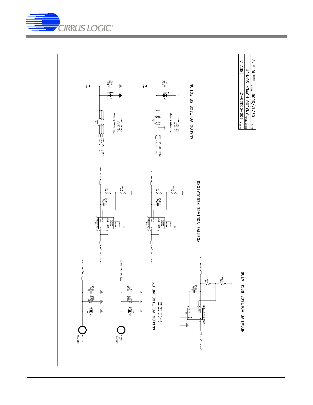
CDB5374
DS862DB1 77
Page 78
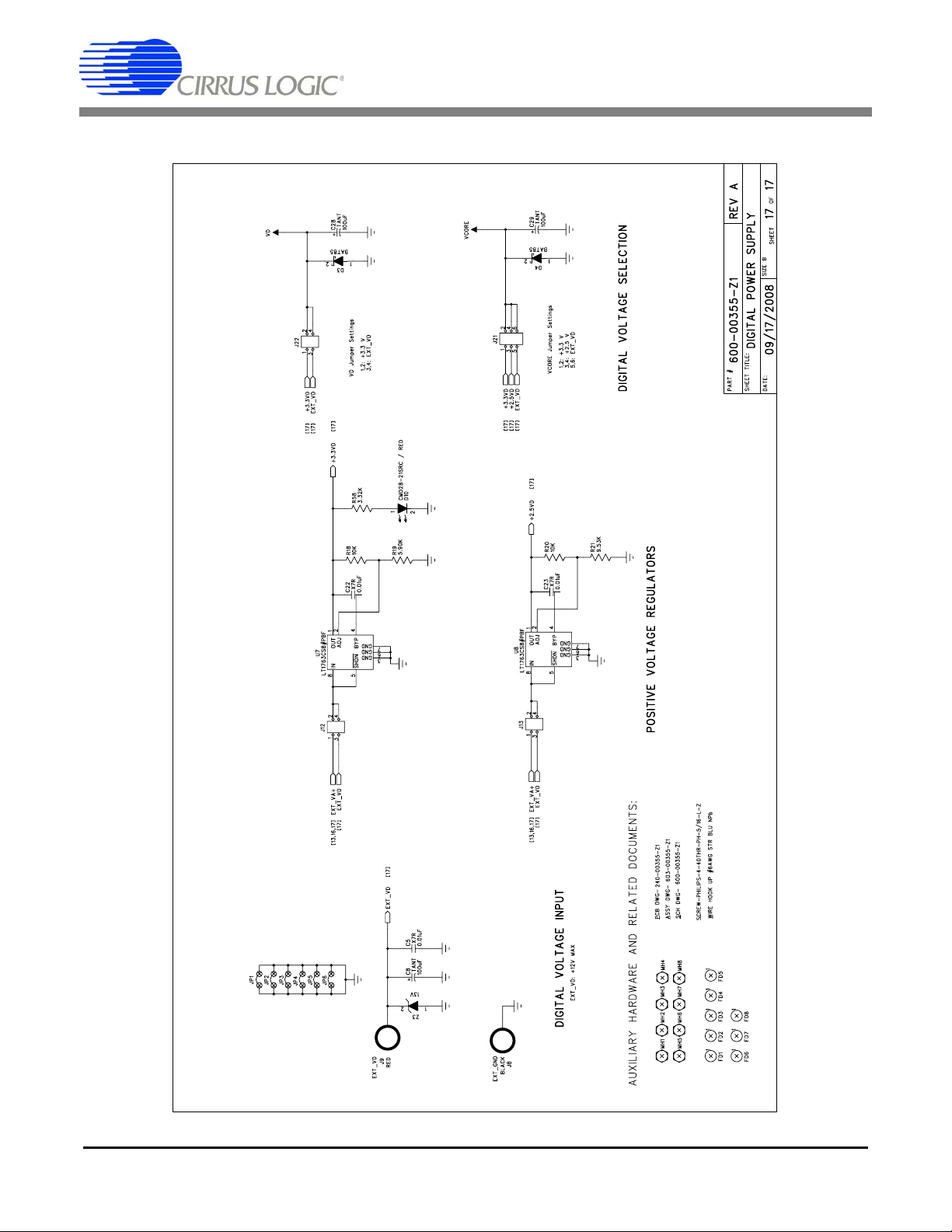
CDB5374
78 DS862DB1
 Loading...