

Page 1
Evaluation Board for CS5366
CDB5366
Features
! Single-Ended to Differential Analog Inputs
! 3.3 V Logic Interface
! Connection for DSP Serial I/O
! Windows®-Compatible CDB5366 Software
Supplied by Cirrus to Configure the
!
On-Board CS8406 to Generate S/PDIF and
EIAJ-340 Digital Audio
! Requires Only an Analog Signal Source, Power
Supplies and, optionally, a PC for a Complete
Analog-to-Digital-Converter Evaluation System
RS232
USB
CS5366
8051 Micro
Description
The CDB5366 evaluation board is an excellent means
for quickly evaluating the CS5366 24-bit, 192 kHz A/D
converter. Evaluation requires only a digital signal analyzer, an analog signal source, and a power supply.
On-board DIP switches configure the CS5366 in StandAlone mode, avoiding the need for a PC.
For software-based device configuration, the Control
Port mode is used by attaching a host PC to the Evaluation Board and executing the provided FlexGUI
software.
ORDERING INFORMATION
CDB5366 Evaluation Board
RCA
Jacks
http://www.cirrus.com
6
Analog
Input
Buffers
6
6
Control
I²C or SPI
CS5366 A/D
Ain+
Ain-
Clks/Data
Buffers
Audio
Clks/Data
Copyright © Cirrus Logic, Inc. 2005
(All Rights Reserved)
FPGA
CS8406
AES/EBU
S/PDIF
Transmitter
S/PDIF
Output
Optical
Coaxial
SEPTEMBER '05
DS626DB1
Page 2

TABLE OF CONTENTS
1. CDB5366 System Overview..................................................................................................................... 3
2. Quick-Start Guide..................................................................................................................................... 3
3. Detailed Board Features.................................................................. ........................................................ 3
3.1 Stand-Alone Evaluation ............................................................................................................ 3
3.1.1 S1 and S4 Switch Operation .................................................. ... ... .... ... ... ... ... .... ... ... ... .... . 4
3.2 Control-Port Evaluation ............................................................................................................ 5
3.3 FlexGUI Hi-Level View ............................................................................................................. 6
3.4 FlexGUI Low-Level View .......................................................................................................... 7
3.5 Bit Definitions ........................................................................................................................... 8
3.5.1 CS5366 Bits ....................................................................................................................8
3.5.2 FPGA Bits ....................................................................................................................... 8
4. CDB5366 Hardware................................................................................................................................. 9
4.1 Input and Output Connectors ................................................................................................... 9
4.2 Switches ................................................................................................................................. 10
4.3 User Configuration Jumpers .................................................................................................. 10
4.4 Reserved Factory Programming Jumpers ............................................................................. 10
4.5 Power Supply Circuitry ........................................................................................................... 11
4.6 Grounding and Power Supply Treatment ............................... ................................................ 11
4.7 FPGA Hardware ..................................................................................................................... 11
4.8 CS8406 S/PDIF Audio Transmitter ........................................................................................ 11
4.9 Serial Audio Interface ............................................................................................................. 11
4.10 Analog Input Buffer .............................. ... ... .... ... ....................................... ... ......................... 11
5. Schematics............................................................................................................................................. 12
6. Board Layout and Routing Plots ........................................................................................................... 21
7. Revision History..................................................................................................................................... 24
CDB5366
LIST OF FIGURES
Figure 1. Hi-Level FlexGUI View ................................................................................................................. 6
Figure 2. FlexGUI Low-Level Register View ............................................................................................... 7
Figure 3. FPGA Low-Level Bit View ............................................................................................................ 8
Figure 4. CS5366 (Schematic page 1) ...................................................................................................... 12
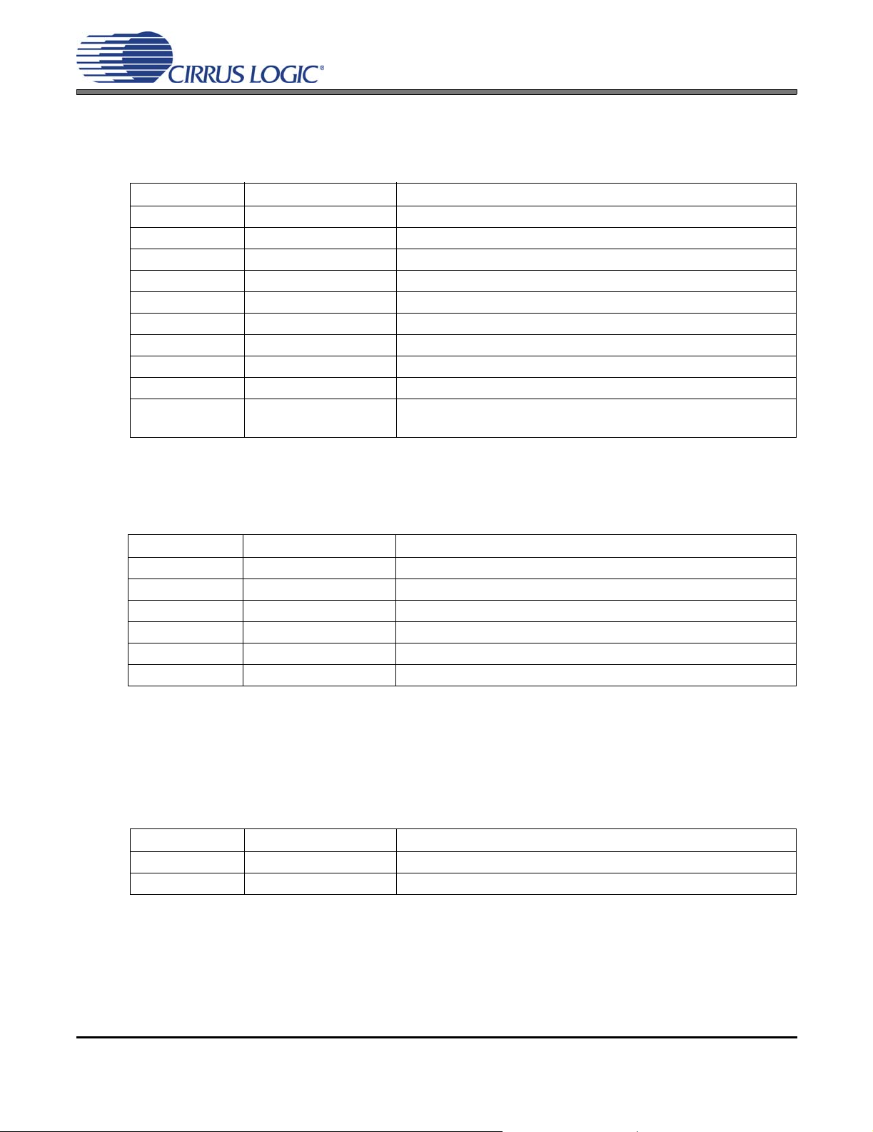
Figure 5. Clock Generation (Schematic page 2) ....................................................................................... 13
Figure 6. FPGA (Schematic page 3) ......................................................................................................... 14
Figure 7. Control Port (Schematic page 4) ................................................................................................ 15
Figure 8. Clock and Data Buffers (Schematic page 5) .............................................................................. 16
Figure 9. CD8406 S/PDIF Output (Schematic page 6) ............................................................................. 17
Figure 10. Analog Inputs 1 to 4 (Schematic page 7) ................................................................................. 18
Figure 11. Analog Inputs 5 to 8 (Schematic page 8) ................................................................................. 19
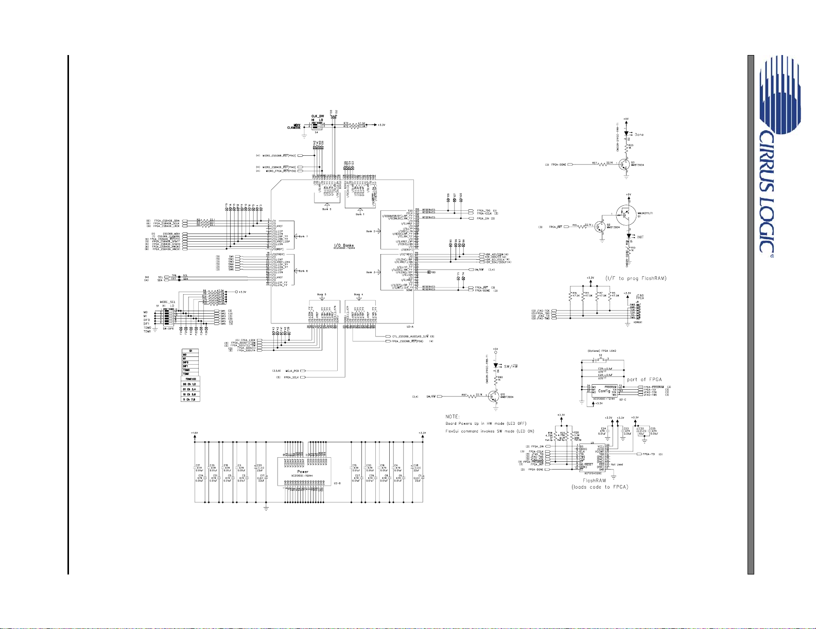
Figure 12. Power (Schematic page 9) ....................................................................................................... 20
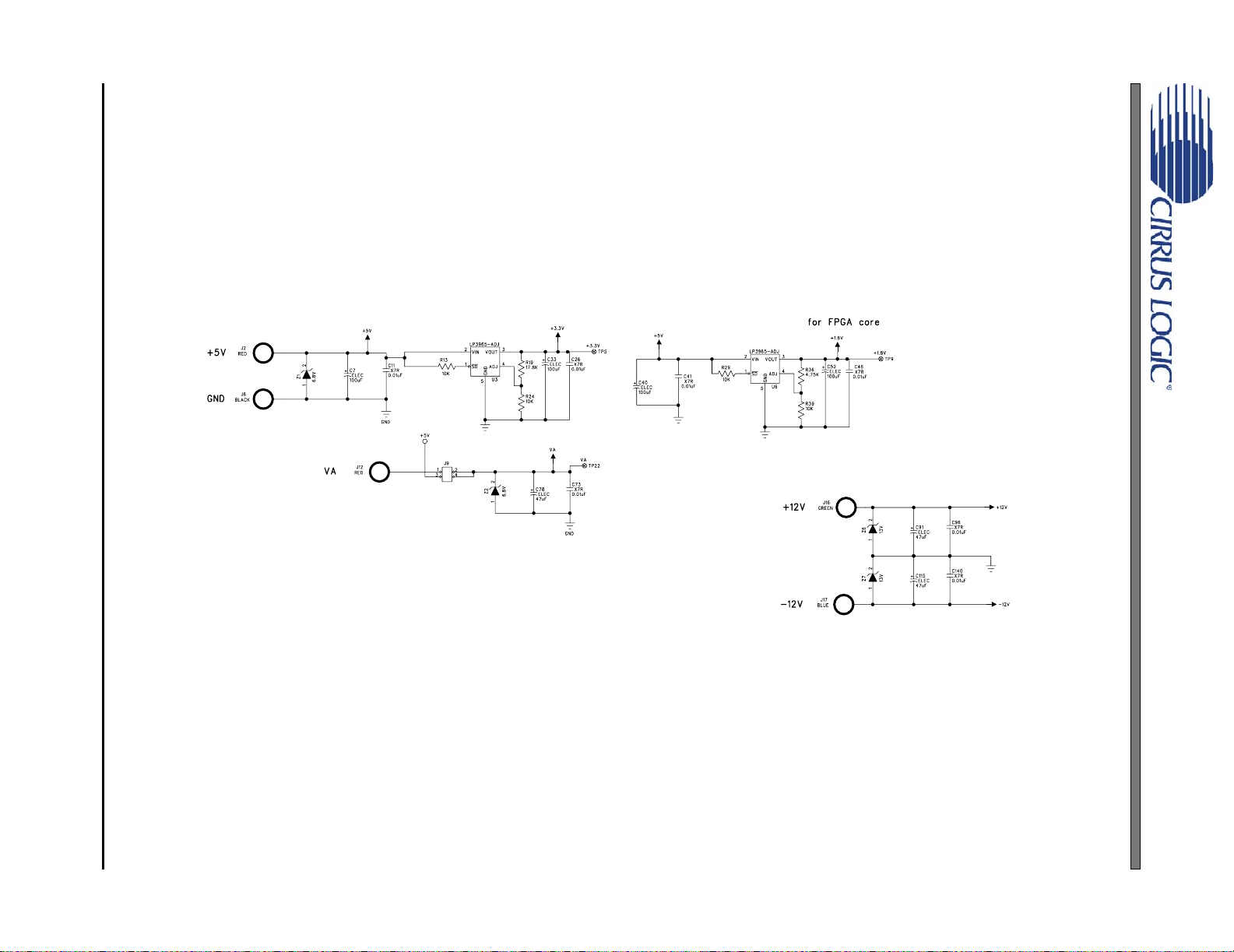
Figure 13. Top Silkscreen ......................................................................................................................... 21
Figure 14. Top Layer ................................................................................................................................. 22
Figure 15. Bottom Layer ......................... ... ... ... ... .... ... ... ....................................... ...................................... 23
LIST OF TABLES
Table 1. CDB5366 Input and Output Connectors ....................................................................................... 9
Table 2. CDB5366 Switches ..................................................................................................................... 10
Table 3. User Jumpers .............................................................................................................................. 10
Table 4. CDB5366 Reserved Jumpers ..................................................................................................... 10
2 DS626DB1
Page 3

CDB5366
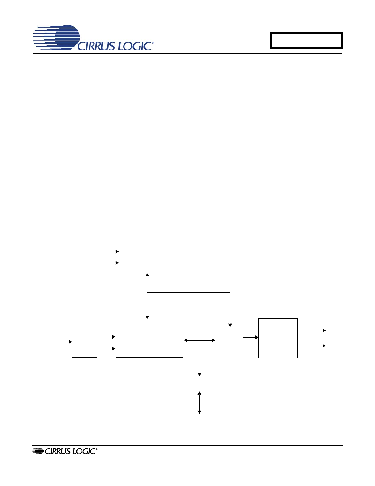
1. CDB5366 SYSTEM OVERVIEW
The CDB5366 Evaluation Board provides an excellent means of quickly evaluating the CS5366. A digital audio interface transmitter (CS8406) provides an easy interface to digital audio signal analyzers, including the majority of
digital audio test equipment. Standard analog input and digital output conn ectors are included for quick and re liable
board setup. An on-board FPGA is used for confi guring the vari ous modes of the CS53 66. Graphica l User Interface
software is supplied by Cirrus Logic, which allows programming the CDB5366 when connected to a host PC run ning
Microsoft Windows
®
.
2. QUICK-START GUIDE
• Confirm that DIP switches S1 and S4 are in the closed (LO) position, pushed down to the right.
• Connect the following jumpers.
– J7 - Install 5 jumpers to the left side of J7, enabling the DIP switches to operate correctly.
– J81, J95 - Install jumpers to these positions, grounding XTI and XTO of the CS5366.
– J1 - Install a jumper at the +5 V position, allowing VA to be supplied by the +5 V supply.
• Install a 12.288 MHz canned Oscillator to socket Y1, providing a Master Timing Clock for the system.
• Install a jumper to J11 at the OSC position to enable the OSC drive buffer.
• Connect power supply common to the GND binding post. Connect +5 V, +12 V and -12 V to the binding
posts as marked on the board silkscreen
This configuration provides a completely operational 24-bit Analog-to-Digital-Converter evaluation system. The
CS5366 is operating as a Master Device in Single S peed Mod e with a 48 kHz sampling rate. Apply power and connect analog input signals of 1 Vrms maximum (full scale) to the RCA inputs jacks. S/PDIF Digital audio data is available for evaluation at the Optical and Coaxial outputs.
3. DETAILED BOARD FEATURES
The CDB5366 Evaluation Board supports both the Stand-Alone and Control Port modes of the CS5366. An FPGA
(U2) controls digital signal routing between the CS5 366, the CS8406 and the DSP I/O header. For user-friendly evaluation of the TDM interface, the FPGA will translate TDM data into PCM data and send it to the CS8406.
3.1 Stand-Alone Evaluation
In Stand-Alone mode, the CDB5366 runs without an external PC attached. In this mode, the FPGA controls
operation of the board by dynamically reading DIP switches (S1 and S4) after a cold power-up or a pushbutton board reset. Stand-Alone mode provides the most commonly used device settings. For additional
control of the CS5366, Control Port mode is used.
In Stand-Alone mode, as the DIP switches are repositioned , the FPGA sim ultaneously sets the app ropriate
pins on the CS5366 and CS8406 to keep them synchronized with regard to sampling speed and data format.
DS626DB1 3
Page 4

3.1.1 S1 and S4 Switch Operation
DIP Switch S1 contains six switches that function as described below.
M1,M0 set the device Speed Mode
0x00 Single Speed Master
0x01 Double Speed Master
0x10 Quad Speed Master
0x11 Slave all speed
DIF1,DIF0 set the Digital Audio Interface Data form at
0x00 Left Justified
0x01 I²S
0x10 TDM 2-wire
0x11 TDM 4-wire
TDM1 and TDM0 support both TDM mode and PCM mode.
In TDM mode, TDM1 and TDM0 select two stereo pairs from a TDM stream, convert the data to Left-Jus-
tified PCM format then send the data to the CS8406 S/PDIF transmitter.
0x00 TDM Pair 1 (Channel 1, 2)
0x01 TDM Pair 2 (Channel 3, 4)
0x10 TDM Pair 3 (Channel 5, 6)
0x11 Reserved
CDB5366
In PCM mode, TDM1 and TDM0 select which SDOUT is sent to the CS8406.
0x00 SDOUT1 (Channel 1, 2)
0x01 SDOUT2 (Channel 3, 4)
0x10 SDOUT3 (Channel 5, 6)
0x11 Reserved
DIP Switch S4 contains two switches which function as described below.7
MDIV - divides the master clock by 2 when OPEN (HI).
CLKMODE - divides the master clock by 1.5 when OPEN (HI)
4 DS626DB1
Page 5

3.2 Control-Port Evaluation
The CDB5366 is shipped with a Cirrus Logic designed Microsoft Windows-based program that allows full
control over the CS5366 internal registers. This software pr ogram is calle d the FlexGUI, a nd it is loade d by
executing the FlexLoader.exe file. Hardware interface to the Fl exGUI is provide d by connecting an RS-232
cable or a USB cable between a host PC and the CDB5366. Once the FlexGUI is loaded, the Evaluation
Board DIP switches are ignored, and all register settings are available for re ading and writing using software
control. Testing configurations may be quickly reproduced by using the Fle xGUI to save and restore unique
register settings.
Configure the board for Control Port op er a tion using the instructions that follow.
• Connect jumpers.
– J7 - Install 5 jumpers to the left side of J7, enabling the I²C control interface.
– J81, J95 - Install jumpers to these positions, grounding XTI and XTO of the CS5366.
– J9 - Install a jumper at the +5 V position, allowing VA to be supplied by the +5 V supply (VA may be
externally supplied at the VA binding post by moving jumper J9 to the VA EXT position).
• Add an oscillator of choice to socket Y1 to provide a Master Timing Clock for the system. A crystal may
also be used by removing the canned oscillator and jumpers J81, J95 and J11. The CDB5366 Evaluation
Board is shipped with 39 pF loading capacitors for crystal-based oscillators. Soldering pads are provided
on the board for users that require third overtone tank circuit operation or different loading capacitors.
CDB5366
• Connect the power supply common to the GND binding post. Connect +5 V, +12 V and -12 V to the bind-
ing posts as marked on the board silkscreen.
The FlexGUI provides two convenient views of the CDB5366 Evaluation Board settings. The default view is
a high-level functional mapping of settings. The second view is a lower -level register map view for progr amming at the bit level. Each view is synchronized with the other view, so that changing a setting at one level
will also change the corresponding setting in the alternate level.
DS626DB1 5
Page 6
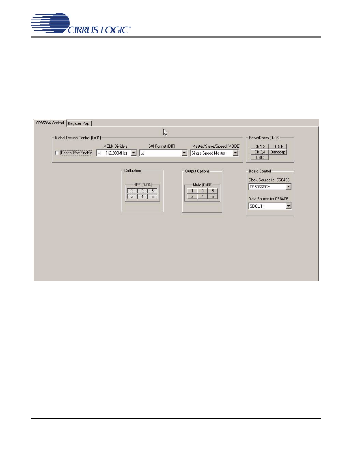
3.3 FlexGUI Hi-Level View
The Cirrus Logic FlexGUI defaults to the Hi-Level View as shown in Figure 1. This view provides functionally
grouped control over the CS5366, reducing the need to memorize the exa ct location of bit settings. Any register may be modified at any time; however, the effect of changes made to the CS53 66 is gated off u ntil the
Control Port Bit is enabled.
When switching to TDM mode, the CS8406 Clock and Date source (Board Con trol Panel) must be chang ed
prior to changing the CS5366 SAI format. This sequential orderin g re se ts th e F PG A t o a ss ur e th at it t ime d
properly with the CS5366 TDM packet stream.
CDB5366
Figure 1. Hi-Level FlexGUI View
6 DS626DB1
Page 7
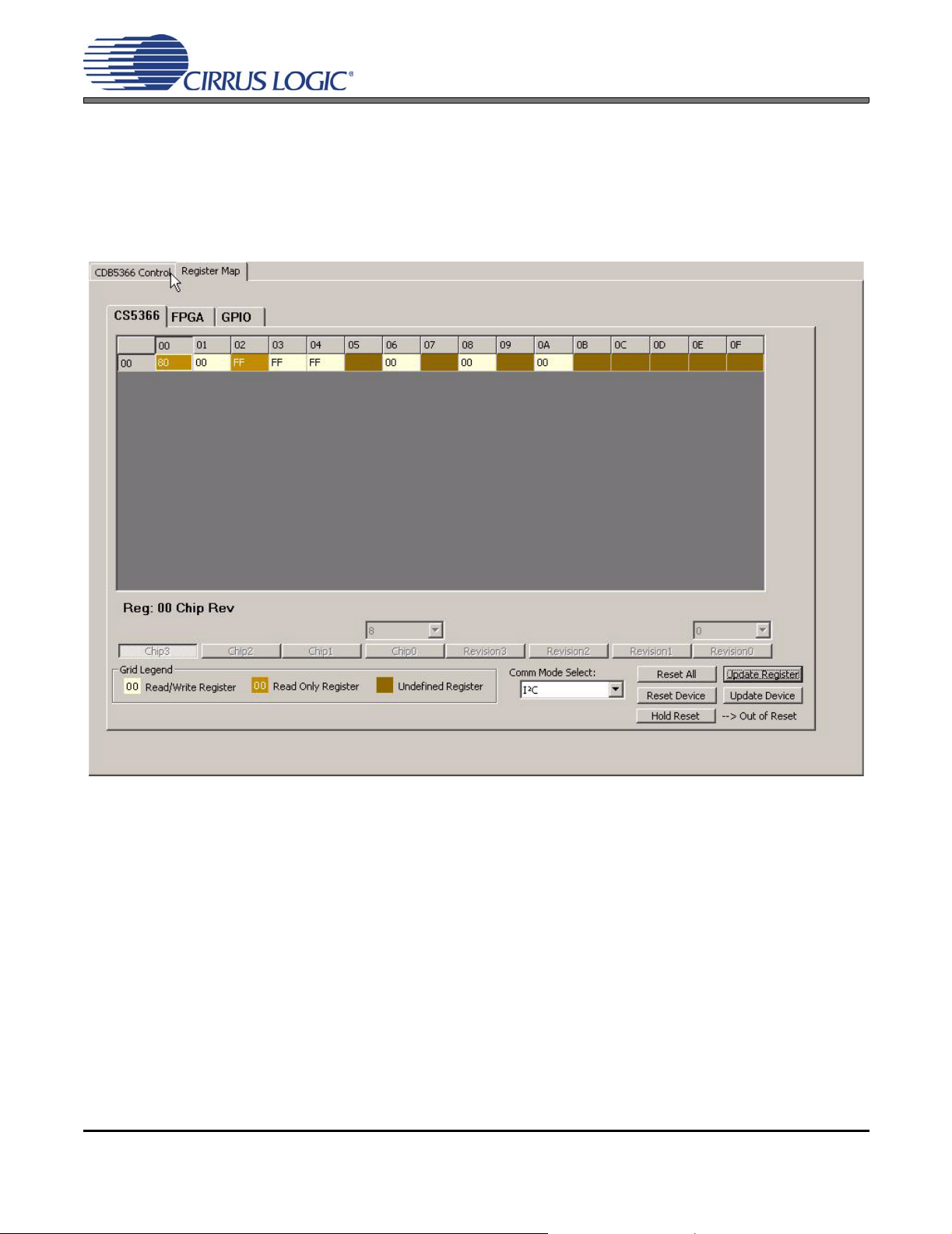
3.4 FlexGUI Low-Level View
The Low-level Register Map view provides direct control over the CS5366, the FPGA and GPIO settings
that change the CS5366 device address. Select the desired device tab; then select and modify any writeregister values. Register modification is always a READ-WRITE-READ operation and is usable at both the
byte or bit level. For byte-level control, type the required hex value in the desired register field numerical
box. For bit-level control, click the corresponding graphical push-button in the desired register field or use
the pull-down menu to access and change the bit values.
CDB5366
Figure 2. FlexGUI Low-Level Register View
When the CS5366 is put in Control Port mode , the DIP switches are ignored and configuration is determined
by the register bits. When placed back in Stand-Alone mode, the DIP switches regain board co ntrol. Exiting
Control Port mode is achieved by stopping the Flex GUI program. Once the prog ram is stopped, about th ree
seconds later, Stand-Alone mode is established.
DS626DB1 7
Page 8
3.5 Bit Definitions
3.5.1 CS5366 Bits
The Low-Level view of the FlexGUI provides the full register set of the CS5366 under the CS5366 tab.
The CS5366 datasheet provides full details of internal register operation.
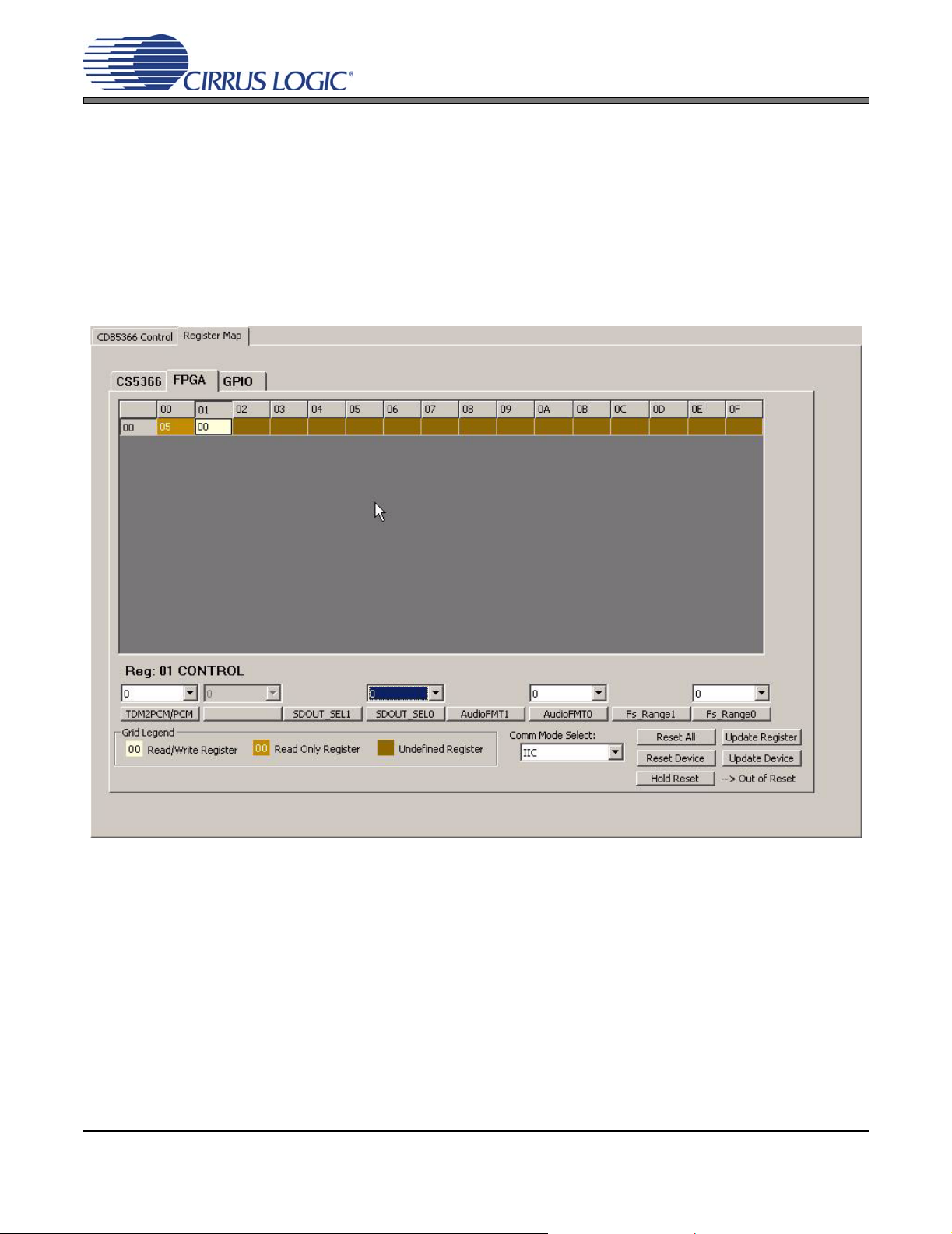
3.5.2 FPGA Bits
FPGA Register 0x00 is non-functional and only contains the revision code of the FPGA.
FPGA Register 0x01 is a functional register that provides the following functionality.
CDB5366
Figure 3. FPGA Low-Level Bit View
Fs_Range1,0 set the device Speed Mode. These bits need to be changed when using the Serial Audio
Interface of the DSP header to communicate with external equipment.
0x00 Single Speed Master
0x01 Double Speed Master
0x10 Quad Speed Master
0x11 Slave all speed
AudioFMT1,0 set the Serial Audio Interface format when attaching the Serial Audio Interface of the DSP
header to external equipment.
0x00 Left Justified
0x01 I²S
0x10 TDM 2-wire
0x11 TDM 4-wire
8 DS626DB1
Page 9

CDB5366
In TDM mode, SDOUT_SEL1 and SDOUT_SEL 0 extract two stereo pairs from the CS5366 TDM stream,
convert the data to Left-Justified PCM format and send the data to the CS8406 data input pin.
0x00 TDM Pair 1 (Channel 1, 2)
0x01 TDM Pair 2 (Channel 3, 4)
0x10 TDM Pair 3 (Channel 5, 6)
0x11 Reserved
In PCM mode, SDOUT_SEL1 and SDOUT_SEL 0 select which SDOUT pin of the CS5366 is sent to the
CS8406.
0x00 SDOUT1 (Channel 1, 2)
0x01 SDOUT2 (Channel 3, 4)
0x10 SDOUT3 (Channel 5, 6)
0x11 Reserved
TDM2PCM/PCM selects the clock source for the CS8406.
0x00 8406 Clock Source is CS5366
0x01 8406 Clock Source is the FPGA TDM2PCM engine
4. CDB5366 HARDWARE
The CDB5366 Evaluation Board has a number of connections, switches and jumpers that provide ease and convenience for quickly evaluating the most commonly used functions of the CS5366 silicon device. The following tables
list the purpose of each hardware option on the Evaluation Board.
4.1 Input and Output Connectors
The input and output conne ctors prov ide power an d signal connectivit y to the CDB536 6 Evaluatio n Board
as shown in Table 1.
DESIGNATOR NAME CLASS FUNCTION
J6 GND Ground Ground connection from power supply
J2 +5 V Power + 5 Volt power for CS5366
J16 +12 V Power +12 V power for the active input buffers
J17 -12 V Power -12 V power for the active input buffers
J18 AIN6 Analog Input Analog input channel 6
J19 AIN5 Analog Input Analog input channel 5
J20 AIN1 Analog Input Analog input channel 1
J21 AIN2 Analog Input Analog input channel 2
J22 AIN4 Analog Input Analog input channel 4
J23 AIN3 Analog Input Analog input channel 3
OPT1 Optical Output Digital Output S/PDIF Optical Digital audio output
J3 Coax Output Digital Output S/PDIF Coaxial Digital audio output
J5 RS232 I/O Digital I/O FlexGUI Interface port to PC
J10 USB I/O Digital I/O FlexGUI Interface port to PC
T able 1. CDB5366 Input and Output Connectors
DS626DB1 9
Page 10
4.2 Switches
The CDB5366 Evaluation Board switches are used for setting speed modes and format protocols and for
resetting devices to their default state. The switch functions are described in Table 2.
.
DESIGNATOR NAME FUNCTION (see CS5366 Datasheet for details)
S1-1 M0 speed mode; Master/Slave function
S1-2 M1 speed mode; Master/Slave function
S1-3 DIF0 Data Format
S1-4 DIF1 Data Format
S1-5 TDM0 Select Channel pairs for S/PDIF output
S1-6 TDM1 Select Channel pairs for S/PDIF output
S4-1 MDIV Master Clock Divider
S4-2 CLKMODE Master Clock Divider
S3 BOARD RESET Resets CS5366, CS8406 and FPGA
S2 PGM Forces FPGA to be loaded with new code (not needed by
Table 2. CDB5366 Switches
4.3 User Configuration Jumpers
CDB5366
user)
The CDB5366 Evaluation Board jumpers are used for signal routing as shown in Table 3
.
DESIGNATOR NAME FUNCTION
J7 CONTROL Select I²C control Source
J91 - Short to ground when not using Crystal
J85 - Short to ground when not using Crystal
J11 OSC/XTL Canned Oscillator/Crystal Selection
J9 +5 V/VA EXT VA source selector
J4 DSP HEADER
Table 3. User Jumpers
4.4 Reserved Factory Programming Jumpers
The CDB5366 Evaluation Board has two reserved headers, J15 and J8, that are used to factory program
the Cygnal
Caution! Do not apply power or shorts to these two jumpers as device damage could occur.
.
DESIGNATOR NAME FUNCTION
J15 MICRO_PROG Reserved interface for pre-programming the Evaluation Board
J8 JTAG Reserved interface for pre-programming the Evaluation Board
®
8051 microprocessor and the Xilinx® FPGA so that the FlexGUI interface operates correctly.
Table 4. CDB5366 Reserved Jumpers
10 DS626DB1
Page 11

4.5 Power Supply Circuitry
Power is applied to the evaluation board through five binding posts (+5 V, +12 V, -12 V, VA and GND). The
GND connection is the common reference for power supplies. The +5 V binding post supplies digital power
for all logic devices. The +12 V and -12 V binding posts supply power for the Operational Amplifier input
buffers. The VA binding posts supplies power to the Analog Reference.
4.6 Grounding and Power Supply Treatment
As a high-peformance mixed-signal device, the CS5366 requires careful attention to power and grounding
arrangements to optimize CS5366 performance. The CDB5366 Evaluation Board provides an excellent reference example of an optimum two-layer board layout that places decoupling capacitors as cl ose to the
CS5366 as possible and provides ground plane fill on both top and bottom layers.
4.7 FPGA Hardware
The on-board FPGA is utilized for several purposes. In addition to providing a method for configuring the
CS5366 in Software mode, it contains its own configuration registers that provide clo ck and data routing for
Master and Slave modes of the CS5366. The FPGA contains a multiplexer that selects which SDOUT line
is routed to the CS8406. It also contains a TDM2PCM engine that extracts channel pairs from a TDM stream
and sends them to the CS8406.
4.8 CS8406 S/PDIF Audio Transmitter
CDB5366
The system generates standard S/PDIF data using a CS8406 192 kHz Digital Audio Transmitter. The
CS8406 receives input data from the F PG A in P CM format and transmits S/PDIF data on both optical and
coaxial output connectors. The optica l outpu t conn ector is limited to a maximum speed of 96 kHz. The coaxial connector supports Quad Speed 192 kHz clocking rates.
4.9 Serial Audio Interface
In addition to the standard S/PDIF outputs, the Customer Evaluation Board has been designed to allow
Master and Slave operation using the Serial Audio Interface (SAI) via the 14-p in header, J4, which includes
the signals MCLK, SCLK, LRCK, and the four serial data lines.
When the CS5366 is in Slave mode, SCLK and LRCK/FS must be su pplied externally th rough the J4 header.
4.10 Analog Input Buffer
The CDB5366 includes an example of an active low-noise, single-ended-to-differential analog input buffer
shown in the schematic drawings, Figures 10 and 11. Alternate active or passive, single-ended or differential topologies may be used as cost dictates. However, the high performance of the CS5366 may be compromised. Optimum device performance is met by buffering the CS5366 with a low noise structure that is
stable with a 2700 pF output load.
DS626DB1 11
Page 12

12 DS626DB1
5. SCHEMATICS
Figure 4. CS5366 (Schematic page 1)
CDB5366
Page 13

DS626DB1 13
Figure 5. Clock Generation (Schematic page 2)
CDB5366
Page 14
14 DS626DB1
Figure 6. FPGA (Schematic page 3)
CDB5366
Page 15

DS626DB1 15
Figure 7. Control Port (Schematic page 4)
CDB5366
Page 16

16 DS626DB1
Figure 8. Clock and Data Buffers (Schematic page 5)
CDB5366
Page 17

17 DS626DB1
Figure 9. CD8406 S/PDIF Output (Schematic page 6)
CDB5366
Page 18

DS626DB1 18
Figure 10. Analog Inputs 1 to 4 (Schematic page 7)
CDB5366
Page 19

19 DS626DB1
Figure 11. Analog Inputs 5 to 8 (Schematic page 8)
CDB5366
Page 20
DS626DB1 20
Figure 12. Power (Schematic page 9)
CDB5366
Page 21
21 DS626DB1
6. BOARD LAYOUT AND ROUTING PLOTS
Figure 13. Top Silkscreen
CDB5366
Page 22

22 DS626DB1
Figure 14. Top Layer
CDB5366
Page 23

DS626DB1 23
Figure 15. Bottom Layer
CDB5366
Page 24

7. REVISION HISTORY
Release Date Changes
DB1 September 2005 Initial Release
CDB5366
Contacting Cirrus Logic Support
For all product questions and inquiries contact a Cirrus Logic Sales Representative.
To find one nearest you go to <http://www.cirrus.com/corporate/contacts/sales.cfm>
IMPORTANT NOTICE
Cirrus Logic, Inc. and it s su bsi di ar i es ( " Ci r ru s" ) bel i eve that the information cont ai ne d in thi s docu ment i s acc u rat e an d r el i ab le . Ho wever , th e in fo rmat io n i s subj ect
to change without not ice and i s provi ded "AS I S" witho ut warrant y of an y kind ( express o r implie d). Cust omers are a dvised t o obtain the latest version of relevant
information to verify, before placing orders, that information being relied on is current and complete. All products are sold subject to the terms and conditions of sale
supplied at the time of order acknowledgment, including those pertaining to warranty, indemnification, and limitation of liability. No responsibility is as sumed by Cirrus
for the use of this information, includ ing u se of this i nforma tion a s the basis for m anu facture or sa le of a ny item s, or for in fringement of patents or other rights of third
parties. This document is the property of Cirrus and by furnishing this information, Cirrus grants no license, express or implied under any pate nts, m a sk wo rk r ights,
copyrights, trademarks, trade secrets or other intellectual property rights. Cirrus owns the copyrights associated with the information contained herein and gives consent for copies to be made of the information only for use within your organization with respect to Cirrus integrated circuits or other products of Cirrus. This consent
does not extend to other copying such as copying for general distribution, advertising or promotional purposes, or for creating any work for resale.
CERTAIN APPLICATIONS USING SEMI CONDUCTOR P RODUCT S MAY I NVOL VE PO TENT I AL RI SKS OF DEAT H, PE RS ONAL IN JU RY, OR S EV ERE PRO PERTY OR ENVIRONMENTAL DAMAGE (“CRITICAL APPLICATIONS”). CIRRUS PRODUCTS ARE NOT DESIGNED, AUTHORIZED OR WARRANTED FOR USE
IN AIRCRAFT SYSTEMS, MILITARY APPLICATIONS, PRODUCTS SURGICALLY IMPLANTED INTO THE BODY, AUTOMOTIVE SAFETY OR SECURITY DEVICES, LIFE SUPPORT PRODUCTS OR OTHER CRITICAL APPLICATIONS. INCLUSION OF CIRRUS PRODUCTS IN SUCH APPLICATIONS IS UNDERSTOOD
TO BE FULLY AT THE CUSTOMER’S RISK AND CIRRUS DISCLAIMS AND MAKES NO WARRANTY, EXPRESS, STATUTORY OR IMPLIED, INCLUDING THE
IMPLIED WARRANTIES OF MERCHANTABILITY AND FITNESS FOR PARTICULAR PURPOSE, WITH REGARD TO ANY CIRRUS PRODUCT THAT IS USED
IN SUCH A MANNER. IF THE CUSTOMER OR CUSTOMER’S CUSTOMER USES OR PERMITS THE USE OF CIRRUS PRODUCTS IN CRITICAL APPLICATIONS, CUSTOMER AGREES, BY SUCH USE, TO FULLY INDEMNIFY CIRRUS, ITS OFFICERS, DIRECTORS, EMPLOYEES, DISTRIBUTORS AND OTHER
AGENTS FROM ANY AND ALL LIABILITY, INCLUDING ATTORNEYS’ FEES AND COSTS, THAT MAY RESULT FROM OR ARISE IN CONNECTION WITH
THESE USES.
Cirrus Logic, Cirrus, and the Cirrus Logic logo and designs are trademarks of Cirrus Logic, Inc. All other brand and product names in this document may be trademarks or service marks of their respective owners.
I²C is a registered trademark of Philips Semiconductor.
Microsoft Windows is a registered trademark of Microsoft Corporation.
Cygnal is a registered trademark of Silicon Laboratories, Inc.
Xilinx is a registered trademark of Xilinx, Inc.
24 DS626DB1
 Loading...