Page 1
Evaluation Board for CS5361
CDB5361
Features
Demonstrates recommended layout and
grounding arrangements
CS8406 generates S/PDIF, and EIAJ-340
compatible digital audio
Requires only an analog signal source and
power supplies for a complete Analog-toDigital-Converter system
Description
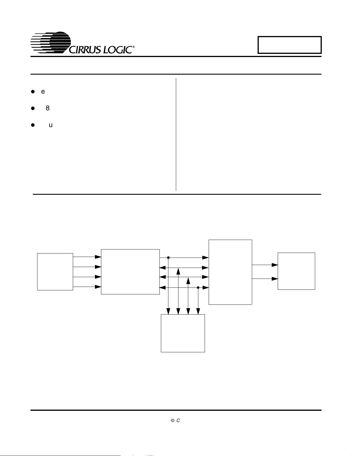
The CDB5361 evaluation board is an excellent means
for quickly evaluating the CS5361 24-bit, stereo A/D converter. Evaluation requires a digital signal analyzer, an
analog signal source, and a power supply.
Also included is a CS8406 digital audio interface transmitter which generates S/PDIF, and EIAJ-340
compatible audio data. The digital audio data is available
via RCA phono and optical connectors.
ORDERING INFORMATION
CDB5361 Evaluation Board
ANALOG
INPUT
Cirrus Logic, Inc.
www.cirrus.com
CS5361
AES/EBU
TRA N SMITTER
I/O FOR
CLOCKS
AND DATA
CopyrightCirrus Logic, Inc. 2003
(All Rights Reserved)
CS8406
S/PDIF
S/PDIF
OUTPUT
FEB ‘03
DS467DB4
1
Page 2

TABLE OF CONTENTS
1. CDB5361 SYSTEM OVERVIEW .............................................................................................. 3
2. CS8406 DIGITAL AUDIO TRANSMITTER ...............................................................................3
3. INPUT/OUTPUT FOR CLOCKS AND DATA ...........................................................................3
4. POWER SUPPLY CIRCUITRY ................................................................................................. 3
5. GROUNDING AND POWER SUPPLY DECOUPLING ............................................................ 3
6. ANALOG INPUT FILTER ......................................................................................................... 3
LIST OF FIGURES
Figure 1. System Block Diagram and Signal Flow .......................................................................... 5
Figure 2. Differential Analog Audio Input......................................................................................... 6
Figure 3. CS5361 ............................................................................................................................ 7
Figure 4. Level Shifters ................................................................................................................... 8
Figure 5. I/O for Clocks/Data........................................................................................................... 9
Figure 6. CS8406 Digital Audio Interface ........................................................................................ 9
Figure 7. Reset Circuit................................................................................................................... 10
Figure 8. Power Circuit.................................................................................................................. 11
Figure 9. Top Layer Silkscreen ..................................................................................................... 12
Figure 10. Top Layer .....................................................................................................................13
Figure 11. Bottom Layer................................................................................................................ 14
CDB5361
LIST OF TABLES
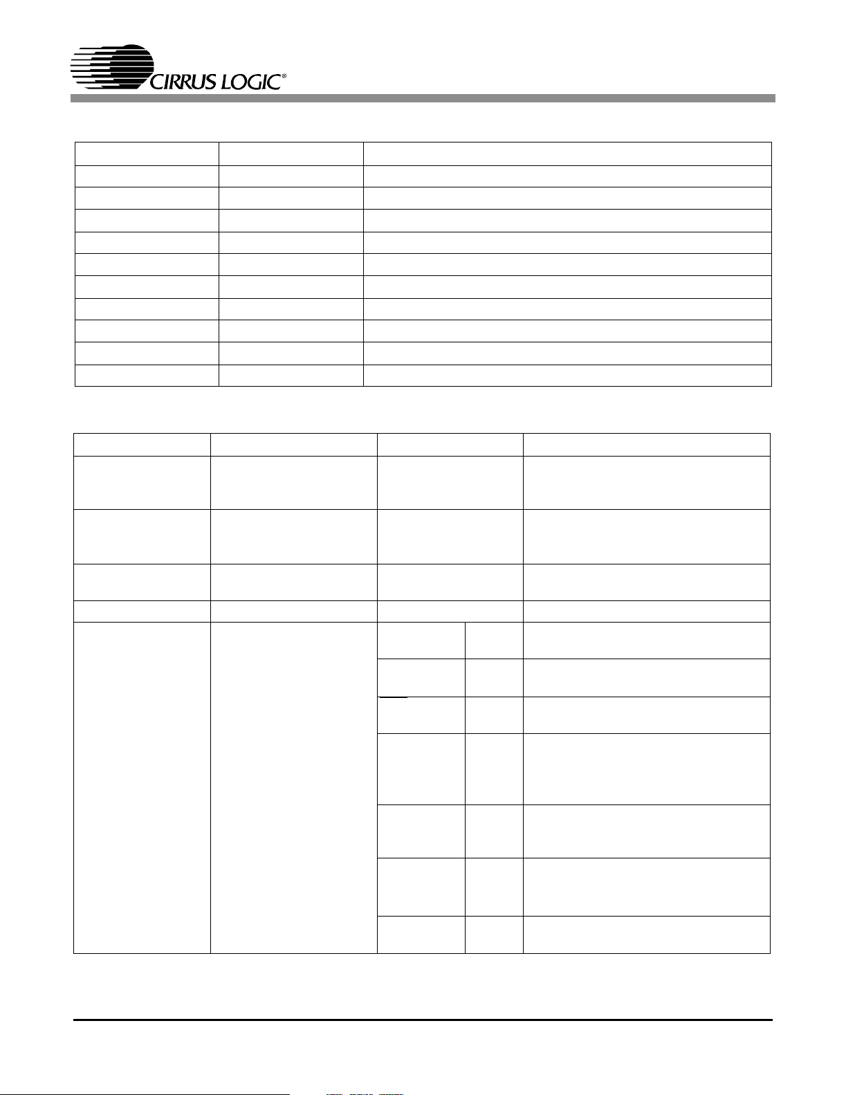
Table 1. System Connections ........................................................................................................4
Table 2. CDB5361 Jumper and Switch Settings ............................................................................ 4
Contacting Cirrus Logic Support
For all product questions and inquiries contact a Cirrus Logic Sales Representative.
To find one nearest you go to www.cirrus.com
IMPORTANT NOTICE
“Preliminary” product information describes product s that are in production, but for which full characteri zation data i s not yet available. “Advance” product information describes products that are in development and subject to development changes. Cirr us Logic, Inc. and its subsidiaries (“Cirrus”) believe that the information contained in this document is accurate and reliable. However, the information is subject to change without notice and is provi ded “AS IS” without warranty
of any kind (express or implied). Customers are advised to obtain the latest version of relevant information to verify, before pl acing orders, that information being
relied on is current and complete. All products are sold subject to the terms and conditions of sale supplied at the time of order acknowledgment, including those
pertaining to warranty, patent infringement, and limitation of liability. No responsibility is assumed by Cir rus f or the use of this information, including use of this
information as the basis for manufacture or sale of any items, or for infringement of patents or other rights of third parties. This document is the property of Cirrus
and by furnishing this information, Cirrus grants no license, express or implied under any patents, mask work rights, copyrights, trademarks, trade secrets or
other intell ectual property ri ghts. Cirrus owns the copyrights associated with the information contained herein and gives consent for copies to be made of the
information only for use within your organization with respect to Cirrus integrated circuits or other parts of Cirrus. This consent does not extend to other copying
such as copying for general distri bution, advertising or promotional purposes, or for creating any work for resale.
An export permit needs to be obtai ned from the competent authorities of the Japanese Government if any of the products or technologies described in thismaterial and controlled under the “Foreign Exchange and Foreign Trade Law” is to be exported or taken out of Japan. An export license and/or quota needs t o be
obtained from the competent authorities of the Chinese Government if any of the products or technologies described in thi s material is subject to the PRC Foreign
Trade Law and is to be exported or taken out of the PRC.
CERTAIN APPLICATIONS USING SEMICONDUCTOR PRODUCTS MAY INVOLVE POTENTIAL RISKS OF DEATH, PERSONAL I NJURY, OR SEVERE
PROPERTY OR ENVIRONMENTAL DAMAGE ( “CRITICAL APPLICATIONS”) . CIRRUS PRODUCTS ARE NOT DESIGNED, AUTHORIZED, OR WARRANTED TO BE SUITABLE FOR USE IN LIFE-SUPPORT DEVICES OR SYSTEMS OR OTHER CRITICAL APPLICATIONS. INCLUSION OF CIRRUS PRODUCTS
IN SUCH APPLICATIONS IS UNDERSTOOD TO BE FULLY AT THE CUSTOMER'S RISK.
Cirrus Logic, Ci rrus, and the Cirrus Logic logo designs are trademarks of Cirrus Logic, Inc. All other brand and product names in this document may be trademarks or service marks of their respective owners.
2 DS467DB4
Page 3

CDB5361
1. CDB5361 SYSTEM OVERVIEW
The CDB5361 evaluation board is an excellent means of quickly evaluating the CS5361. The CS8406 digital audio interface transmitter provides an easy interface to digital audio signal analyzers including the
majority of digital audio test equipment.
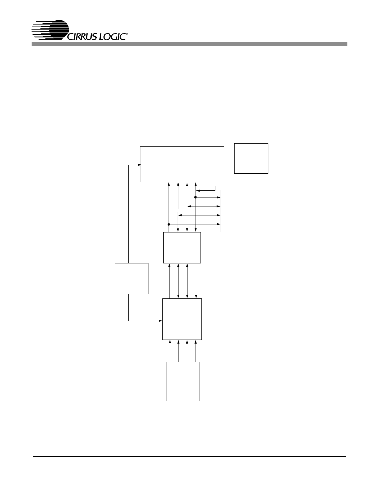
The CDB5361 schematic has been partitioned into 7 schematics shown in Figure 2 through Figure 8.Each
partitioned schematic is represented in the system diagram shown in Figure 1. Notice that the system dia-
gram also includes the interconnections between the partitioned schematics.
2. CS8406 DIGITAL AUDIO TRANSMITTER
The system generates and encodes standard S/PDIF data using a CS8406 Digital Audio Transmitter
(See Figure 6). The outputs of the CS8406 are RS422 compatible differential line drivers. The CS8406
supports both Left Justified and I
the CS8406 is included in the CS8406 datasheet.
3. INPUT/OUTPUT FOR CLOCKS AND DATA
The evaluation board has been designed to allow interfacing to external systems via the 10-pin header, J13.
The schematic for the clock/data input/output is shown in Figure 5.
The CDB5361 allows some flexibility as to the generation of the clocks. When the CS5361 and CS8406
are in slave mode, the SCLK and LRCK must be provided via the header, J13. MCLK must be generated
from the on board oscillator, Y1. This oscillator is socketed to allow other frequency oscillators to be used.
2
S data formats, as determined by the DIP switch, S2. A description of
4. POWER SUPPLY CIRCUITRY
Power is supplied to the evaluation board by six binding posts (-12V, +12V, VD, VL, GND, +5 V),
see Figure 8. -12V and +12V supply the input amplifiers while the VD input supplies the VD pin of the
CS5361. VL supplies power to the VL pin of the CS5361 and to the level shifter circuits. The +5 V input
supplies power to the +5 V digital circuitry and the VA pin of the CS5361.
5. GROUNDING AND POWER SUPPLY DECOUPLING
The CS5361 requires careful attention to power supply and grounding arrangements to optimize performance. Figure 3 details the power distribution used on this board. The decoupling capacitors are located
as close to the CS5361 as possible. Extensive use of ground plane fill in the evaluation board yields large
reductions in radiated noise.
6. ANALOG INPUT FILTER
The CDB5361 implements a fully differential analog input buffer, as shown in Figure 2. Note that there is
no attenuation associated with the input buffer, so a 2Vrms differential input applied at the XLR connectors will provide a full-scale 2Vrms differential input to the CS5361.
DS467DB4 3
Page 4
CDB5361
CONNECTOR INPUT/OUTPUT SIGNAL PRESENT
-12V Input -12V power for the input op-amps
+12V Input +12V power for the input op-amps
VD Input +3.3V to +5V power for the CS5361
VL Input +2.5V to +5V power for the CS5361
GND Input Ground connection from power supply
+5V Input + 5 Volt power
AINL Input Differential analog input left channel
AINR Input Differential analog input right channel
Optical Output Output Digital audio output
Coax Output Output Digital audio output
Table 1. System Connections
JUMPER/SWITCH PURPOSE POSITION FUNCTION SELECTED
J7 VD Power Source ADJ
*+3.3V
+5V
J8 VL Power Source ADJ
*+3.3V
+5V
J13 Input/Output for
clocks/data
S1 Reset for the CDB5361 - -
S2 CDB5361 Configuration M1/M0 Open
--
*ClosedHiLow
ADC *Open
Closed
HPF
DIV Open
IO_HDR Open
DIF Open
8406 Open
Open
*Closed
*Closed
*Closed
*Closed
*Closed
Power from the Binding Post (J3)
Power from the +3.3V Regulator
Power from the +5V Supply
Power from the Binding Post (J4)
Power from the +3.3V Regulator
Power from the +5V Supply
CS5361 in Master mode
CS5361 in Slave mode
High-pass filter is disabled
High-pass filter is enabled
MCLK is divided by two internally by the
CS5361
MCLK is not divided internally by the
CS5361
Header J3 is an input for clocks
Header J3 is an output for clocks and
data
Digital interface format set to I
Digital interface format set to Left Justified
CS8406 in Master mode
CS8406 in Slave mode
2
S
Table 2. CDB5361 Jumper and Switch Settings
* denotes default factory settings
4 DS467DB4
Page 5
CDB5361
R
O
T
A
7
L
L
I
G
I
C
F
S
AUDIO
CS8406
DIGITAL
FIG 6
INTERFACE
CRYSTAL
O
RESET
CIRCUIT
FIG 7
I/O FOR
FIG 4
LEVEL
SHIFTER
3
G
I
CS5361
F
T
L
U
A
I
P
T
N
I
N
E
G
2
R
O
G
E
L
I
F
A
F
F
I
N
A
D
FIG 5
CLOCKS
AND DATA
Figure 1. System Block Diagram and Signal Flow
DS467DB4 5
Page 6

CDB5361
Figure 2. Differential Analog Audio Input
CS5361:
R9, R13, R24, R28 equal 0 ohm
R16, R19 are not installed
6 DS467DB4
Page 7

CDB5361
Z
K
1
6
3
5
S
C
Figure 3. CS5361
DS467DB4 7
Page 8

CDB5361
Figure 4. Level Shifters
8 DS467DB4
Page 9

CDB5361
Figure 5. I/O for Clocks/Data
Figure 6. CS8406 Digital Audio Interface
DS467DB4 9
Page 10

CDB5361
Figure 7. Reset Circuit
10 DS467DB4
Page 11

CDB5361
Figure 8. Power Circuit
DS467DB4 11
Page 12
CDB5361
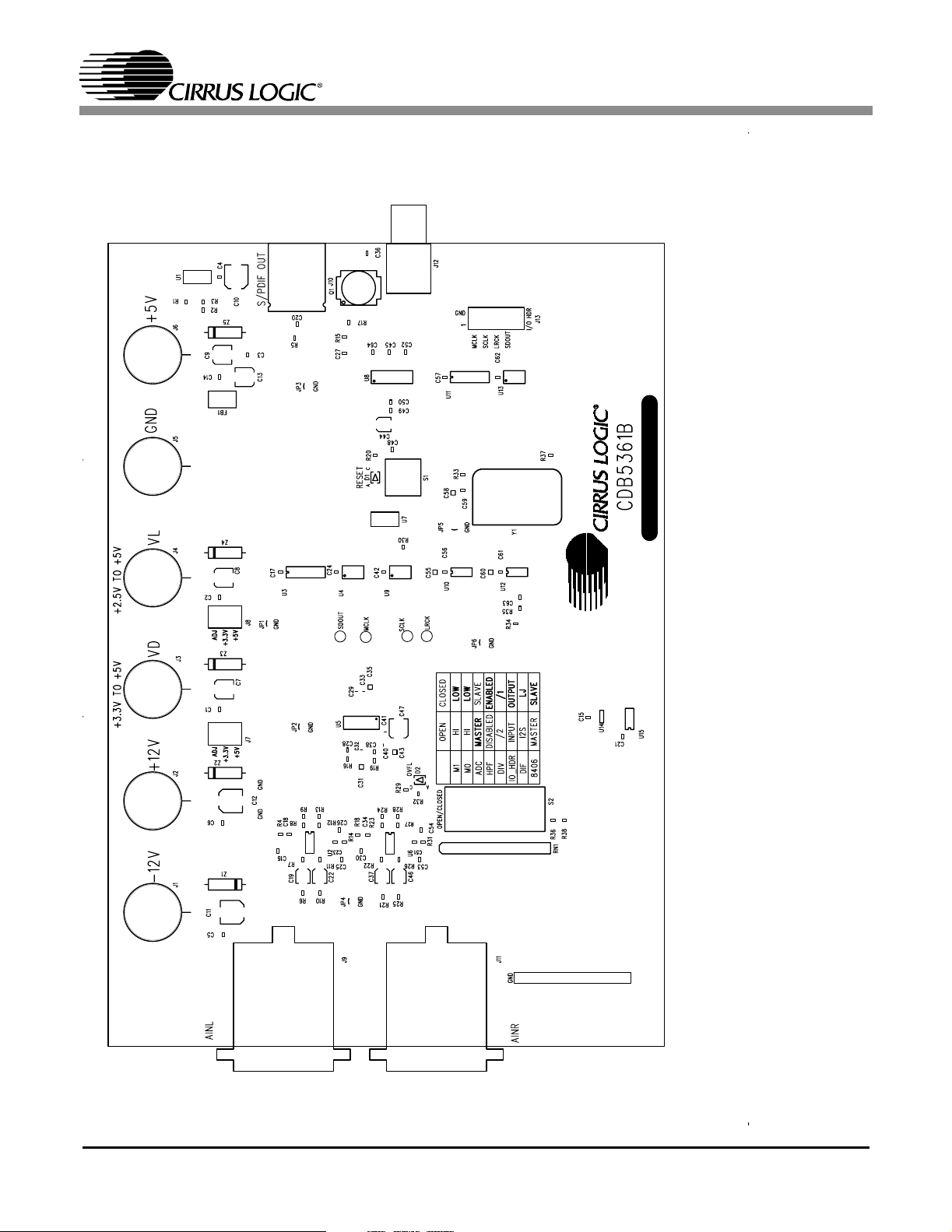
Figure 9. Top Layer Silkscreen
12 DS467DB4
Page 13

CDB5361
Figure 10. Top Layer
DS467DB4 13
Page 14

CDB5361
Figure 11. Bottom Layer
14 DS467DB4
Page 15

• Notes •
Page 16

 Loading...