

Page 1
Evaluation Board for CS5346
CDB5346
Features
Single-ended Analog Inputs
Single-ended Analog Outputs
CS8406 S/PDIF Digital Audio Transmitter
Header for Optional External Software
Configuration of CS5346
Header for External PCM Serial Audio I/O
3.3 V Logic Interface
Pre-defined Software Scripts
Demonstrates Recommended Layout and
Grounding Arrangements
Windows
Configure CS5346 and Inter-board
Connections
®
-compatible Software Interface to
Description
The CDB5346 evaluation board is an excellent means
for evaluating the CS5346 ADC. Evaluation requires an
analog signal source and analog/digital analyzer, and
power supplies. A Windows PC-compatible computer
must be used to evaluate the CS5346.
System timing for the I²S, Left-Justified and Right-Justified interface formats can be provided by the CS5346,
the CS8406, or by the PCM I/O stake header with an e xternal source connected.
RCA phono jacks are provided for the CS5346 analog
inputs and outputs. Digital data input is available via
RCA phono or optical connectors to the CS8406.
The Windows software provides a GUI to make configuration of the CDB5346 easy. The software
communicates through the PC’s USB to configure the
control port registers so that all features of the CS5346
can be evaluated. The evaluation board may also be
configured to accept external timing and data signals for
operation in a user application during system
development.
ORDERING INFORMATION
CDB5346 Evaluation Board
Passive Input Filters
Microphone Inputs
Control Port Interface
http://www.cirrus.com
12
2
2
CS5346
Discrete Buffers
Sub-clocks and Data
Copyright © Cirrus Logic, Inc. 2008
(All Rights Reserved)
Master Clock
Active Output Filter
Test Points
CS2000
Left/Right
Clock
Master
Clock
Header
CS8406
NOV '08
DS861DB1
Page 2

TABLE OF CONTENTS
1. SYSTEM OVERVIEW ............................................................................................................................. 3
1.1 Power ............................................................................................................................................... 3
1.2 Grounding and Power Supply Decoupling ....................................................................................... 3
1.3 CS5346 Audio ADC ......................................................................................................................... 3
1.4 CS8406 Digital Audio Transmitter .................................................................................................... 3
1.5 CS2000 ............................................................................................................................................ 4
1.6 External Control Headers ................................................................................................................. 4
1.7 Analog Inputs ................................................................................................................................... 4
1.8 Analog Outputs ................................................................................................................................ 4
1.9 Serial Control Port ............................................................................................................................ 4
2. SYSTEM CLOCKS AND DATA ........................... ... ... .... ... ... ... .... ... .......................................... ... ........... 5
2.1 Clock Routing ................................................................................................................................... 5
2.2 Data Routing .................................................................................................................................... 5
3. PC SOFTWARE CONTROL ....................... ... .... .......................................... ... ... ..................................... 6
3.1 CDB5346 Controls Tab .................................................................................................................... 6
3.2 Register Maps Tab ........................................................................................................................... 7
3.3 Pre-Configured Script Files .............................................................................................................. 7
3.3.1 12.288MHz, CS5346 Master - ADC Ch 1 In to SPDIF Out ..................................................... 7
3.3.2 12.288MHz, CS8406 Master - ADC Ch 1 In to SPDIF Out ..................................................... 8
3.3.3 12.288MHz, J10 Master - ADC Ch 1 In to SPDIF Out ............................................................ 8
4. CDB CONNECTORS, JUMPERS, AND SWITCHES ..... ... .......................................... ... ... ... .... ... ... ... .... . 9
5. CDB BLOCK DIAGRAM ......................... ... ... .... ... ... ... .... ... ... ................................................................ 10
6. CDB SCHEMATICS ....................... .... ... ... ... ... .... ................................................................................... 11
7. CDB LAYOUT ................... .... ... ... ... .... ... ... ....................................... ... ... ... .... ... ... ... ................................ 16
8. REVISION HISTORY ............................................ ... ... .... ...................................................................... 19
CDB5346
LIST OF FIGURES
Figure 1.CDB5346 Controls Tab ................................................................................................................. 6
Figure 2.Register Maps Tab ............................ ... .... ... ... ... .... ... ... ... .... ... ... ... ... .... ........................................... 7
Figure 3.Block Diagram ............................. ... ... ... .... ... ... ... .......................................... .... ... ......................... 10
Figure 4.CS5346 (Schematic Sheet 1) ..................................................................................................... 11
Figure 5.Analog Inputs/Outputs (Schematic Sheet 2) ............................................................................... 12
Figure 6.USB Microcontroller (Schematic Sheet 3) .................................................................................. 13
Figure 7.S/PDIF and PCM Output (Schematic Sheet 4) . .... .......................................... ... ... ... ... .... ... ... ... ... 14
Figure 8.Power (Schematic Sheet 5) ........................................................................................................ 15
Figure 9.Component Map .................................. .... ... ... ... .... ... ... .......................................... ... ................... 16
Figure 10.Top Layer . .......................................... .... ... .......................................... ... ... ................................ 17
Figure 11.Bottom Layer ................................ ... ... .... .......................................... ... ... ... .... ... ......................... 18
LIST OF TABLES
Table 1. System Connections ..................................................................................................................... 9
Table 2. System Jumper Settings ............................................................................................................... 9
Table 3. Revision History .......................................................................................................................... 19
2 DS861DB1
Page 3

CDB5346
1. SYSTEM OVERVIEW
The CDB5346 evaluation board is an excellent means for evaluating the CS5346 ADC. Analog and digital audio
signal interfaces are provided, a simple bus architecture is used for easily configuring the evaluation platform,
and a USB cable is included for use with the Windows
www.cirrus.com.
The CDB5346 schematic set is shown in Figures 4 through 8. Though the CS5346 device is compatible with the
CS5345 device the CDB5346 platform was not designed to accommodate the CS5345. For CS5345 comparisons
please use the CDB5345.
1.1 Power
Power must be supplied to the evaluation board through the red +5.0 V binding post. An on-board regulator
provides 3.3 V. Appropriate supply levels for powering VA, VD, VLS, and VLC are set by a series of jumpers
(see Table 2 on page 9). All voltage inputs must be referenced to the single black binding post ground connector (see Table 1 on page 9).
WARNING: Please refer to the CS5346 data sheet for allowable voltage levels.
1.2 Grounding and Power Supply Decoupling
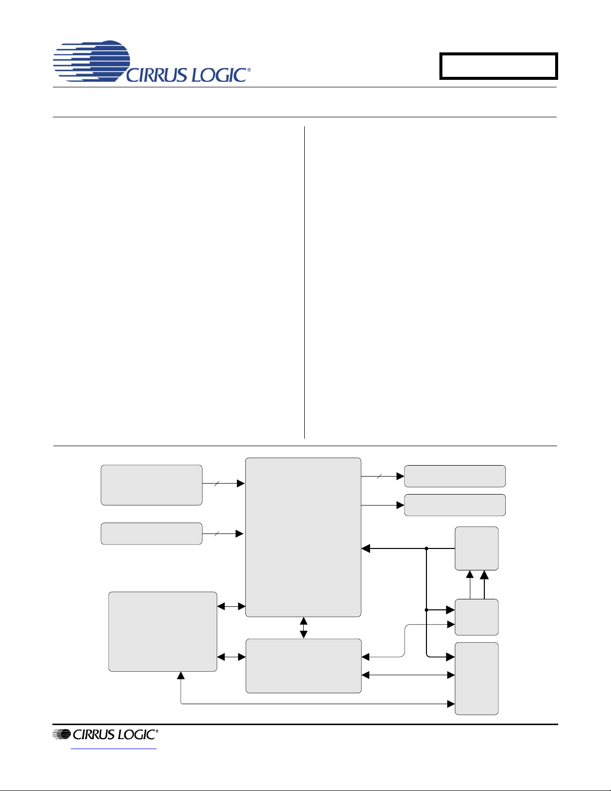
The CS5346 requires careful attention to power supply and grounding arrangements to optimize performance. Figure 3 on page 10 provides an overview of the connections to the CS5346. Figure 9 on page 16
shows the component placement. Figure 10 on page 17 shows the top layout. Figure 11 on page 18 shows
the bottom layout. The decoupling capacitors are located as close to the CS53 46 as possible. Attention h as
been paid to maximize the ground plane fill on the evaluation board. The series resistors on the analog inputs have been placed close to the CS5346 device in order to re duce any unwanted coupling from long traces with high source impedance.
®
configuration software available for download from
1.3 CS5346 Audio ADC
A complete description of the CS5346 is included in the CS5346 product data sheet.
The required configuration settings of the CS5346 are made in its control port registers, accessible through
the CS5346 tab of the Cirrus Logic FlexGUI software.
Clock and data source selectio ns are made through the microcontroller. Basic routing selections can be
made using the CS5346 Controls tab in the GUI software application. Advanced options are accessible
through the Board Configuration sub-tab on the Register Maps tab of the Cirrus Logic FlexGUI software.
1.4 CS8406 Digital Audio Transmitter
A complete description of the CS8406 transmitter (Figure 7 on page 14) and a discussion of the digital audio
interface are included in the CS8406 data sheet.
The CS8406 converts the PCM data generated by the CS5346 to the standard S/PDIF data stream. The
CS8406 can operate in either master or slave mode, accepts 128 Fs, 256 Fs, 384 Fs, and 512 F s master
clocks on the OMCK input pin, and can operate in the Left-Justified, I²S, Right-Justified 16-bit, and RightJustified 24-bit interface formats.
The most common operations of the CS8406 may be controlled via the CDB5346 Controls tab in the GUI
software application. Advanced options are accessible through the CS8406 sub-tab on the Register Maps
tab of the Cirrus Logic FlexGUI software.
DS861DB1 3
Page 4

1.5 CS2000
The CS2000-CP, U7, provides the master clock source to the CDB5346.
The CS2000-CP is a highly configurable clock synthesizer and jitter reducing clock multiplier. Simple scripts
have been pre-configured to generate the necessary configuratio n settings for the CS200 0-CP. For a mo re
in depth look a this device please see the CS2000-CP data sheet.
1.6 External Control Headers
The evaluation board has been designed to allow interfacing with external systems via the headers J19, and
J21.
The 8-pin, 2 row header, J21, provides access to the serial audio signals required to interface to the serial
audio port of the CS5346 with a DSP (see Figure 7 on page 14).
The direction of the signals on header J21 can be configured using the controls located within the Board
Controls group box on the CDB5346 Controls tab in the provided GUI software.
The 15-pin, 3 row header, J19, allows the user bidirectional access to the SPI/I²C control signals by simply
removing all the shunt jumpers from the “PC” position. The user may then cho ose to connect a ribbo n cable
to the “EXTERNAL CONTROL” position. A single “GND” row for the ribbon cable’s ground connection is
provided to maintain signal integrity. Two unpopulated pull-up resistors are also available should the user
choose to use the CDB for the I²C power rail.
CDB5346
1.7 Analog Inputs
RCA connectors supply the CS5346 analog inputs through single-ended, unity gain, passive circuits. Refer
to the CS5346 data sheet for the ADC full-scale input level and input impedance.
1.8 Analog Outputs
The CS5346 PGA analog outputs are routed thr ough a source-followe r op-amp to provide a low impedance
drive and to observe the current draw limitations o f the PGA output pins. The outp ut of the amp is connected
to RCA jacks for easy evaluation.
1.9 Serial Control Port
A graphical user interface is included with the CDB 5346 to allow easy manipu lation of the registers in th e
CS5346, CS8406, and CS2000-CP. See the device-specific data sheets for the CS5346, CD8406, and
CS2000-CP internal register descriptions.
Connecting a USB cable to connector J17 and launching the Cirrus Logic FlexGUI software (FlexLoader.exe) will enable the CDB5346.
Refer to “PC Software Control” on page 6 for a description of the Graphical User Interface (GUI).
4 DS861DB1
Page 5

CDB5346
2. SYSTEM CLOCKS AND DATA
The CDB5346 implements comprehensive clock routing capabilities. Configuration of the clock routing can be easily
achieved using the controls within the Board Controls group box on the CDB5346 Controls tab in the GUI software
application.
2.1 Clock Routing
The master clock signal (MCLK) is always sourced from the CS2000-CP (U18). The CS2000-CP can be
configured to either synthesize a clock from the crystal (Y1) or to be phase locked looped to either the MCLK
or LRCK input from the PCM I/O header (J21).
The sub-clock signals (SCLK and LRCK) may be sourced from the CS5346 in master mode, the CS8406 in
master mode, or the PCM I/O header.
Clock routing configuration is achieved using the controls within the Board Controls group box on the
CDB5346 Controls tab in the GUI software application.
2.2 Data Routing
The serial data output of the CS5346 is routed to both the CS8406 S/PDIF transmitter and the PCM I/O
header. No user configuration of the serial data routing is required.
DS861DB1 5
Page 6
CDB5346
3. PC SOFTWARE CONTROL
The CDB5346 uses a Micro soft Window s-based GUI (download from Cirrus web site), which allows control of the
CS5346, CS8416, CS8406 and CS2000-CP registers. Interface to the GUI is provided via USB connection. Once
the USB cable is connected between the CDB5346 and the host PC, run “FlexLoader.exe”. The software should
automatically detect the board. If a board selection dialog is displayed, select “CDB5346” from the list. Once loaded,
all registers are set to their default state. The GUI’s “File” menu provides the ability to save and load script files containing all of the register settings. Sample script files for basic mode oper ation ca n be down loaded from the a rchive
at www.cirrus.com. Refer to “Pre-Configured Script Files” on page 7 for details.
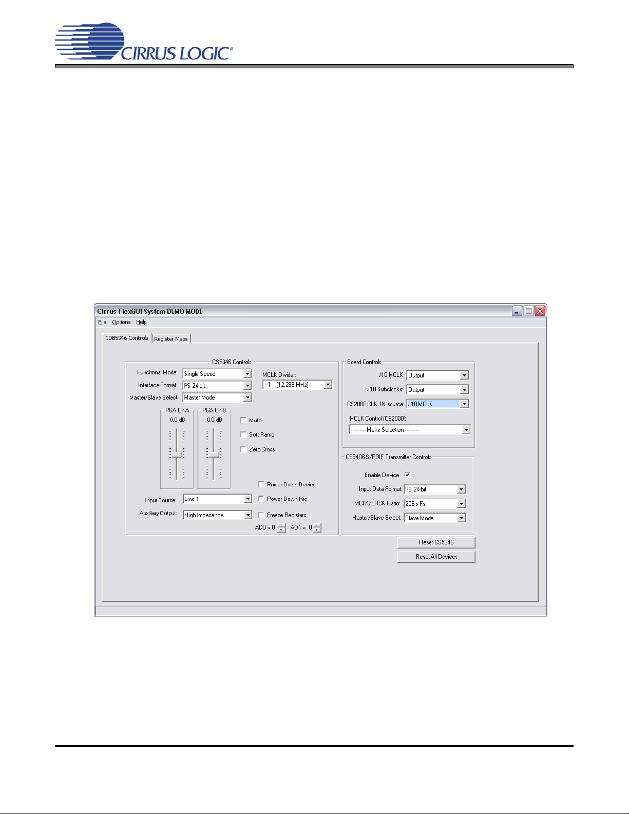
3.1 CDB5346 Controls Tab
The CDB5346 Controls tab provides a high- level intuitive interface to many of the configuration options of
the CS5346 and CDB5346. The controls within the CS5346 Controls gr oup box control the internal registers
of the CS5346 (with the exception of AD0/AD1 which are controlled by GPIO on the on-boar d microcontroller). The controls within the Board Controls group box control the board level clock and data routing on the
CDB5346.
Figure 1. CDB5346 Controls Tab
6 DS861DB1
Page 7

3.2 Register Maps Tab
The Register Maps tab provides low level control over the register level settings of the CS5346, CS8406,
and CS2000-CP. Each device is displayed on a separate tab. Register values can be modified bit-wise or
byte-wise. For bit-wise, click the appropriate push button for the desired bit. For byte-wise, the desired hex
value can be typed directly in the register address box in the register map.
CDB5346
Figure 2. Register Maps Tab
3.3 Pre-Configured Script Files
Pre-configured script files are provided with the CDB5346 to allow easy initial board bring-up. The board
configurations stored within these files are described in sections 3.3.1 - 3.3.2.
3.3.1 12.288MHz, CS5346 Master - ADC Ch 1 In to SPDIF Out
Using the pre-configured script file named “12.288MHz _CS5346 Master_- ADC Ch 1 In to SPDIF
Out.fgs”, an analog input signal applied to channel 1 of the CS5346 input multiplexer will be digitized by
the ADC in Master Mode, transmitted in S/PDIF format by the CS8406. No signal will be output through
the active output filter and RCA jacks.
The CS2000-CP is operated in frequency synthesizer mode to generate the 12.288 MHz master clock.
The CS5346 is the sub-clock master to the CS8406 and the PCM I/O header.
DS861DB1 7
Page 8

3.3.2 12.288MHz, CS8406 Master - ADC Ch 1 In to SPDIF Out
Using the pre-configured script file named “12.288MHz _CS8406 Master_- ADC Ch 1 In to SPDIF
Out.fgs”, an analog input signal applied to channel 1 of the CS5346 input multiplexer will be digitized by
the ADC and transmitted in S/PDIF format by the CS8406 in Master Mode. No signal will be output
through the active output filter and RCA jacks.
The CS2000-CP is operated in frequency synthesizer mode to generate the 12.288 MHz master clock.
The CS8406 is the sub-clock master to the CS5346 and the PCM I/O header.
3.3.3 12.288MHz, J10 Master - ADC Ch 1 In to SPDIF Out
Using the pre-configured script file named “12.288MHz _J10 Master_- ADC Ch 1 In to SPDIF Out.fgs”, an
analog input signal applied to channel 1 of the CS5346 input multiplexer will be digitized by the ADC and
transmitted in S/PDIF format by the CS8406. No signal will be output through the active output filter and
RCA jacks.
The CS2000-CP is operated in frequency synthesizer mode to generate the 12.288 MHz master clock.
The PCM I/O header is the sub-clock master to the CS5346 and the CS8406.
CDB5346
8 DS861DB1
Page 9

4. CDB CONNECTORS, JUMPERS, AND SWITCHES
Reference
CONNECTOR
+5V J22 Input +5.0 V Power Supply
GND J24 Input Ground Reference
S/PDIF TX J20 Output CS8406 digital audio output via coaxial cable
S/PDIF TX OPT1 Output CS8406 digital audio output via optical cable
USB I/O J17 Input/Output USB connection to PC for SPI / I²C control port signals.
PCM I/O J21 Input/Output I/O for Serial Audio Clocks & Data
PC / EXTERNAL
CONTROL
C2 J18 Input/Output I/O for programming the micro controller (U6).
MICRO RESET S1 Input Reset for the micro controller (U6).
AIN1A
AIN1B
AIN2A
AIN2B
AIN3A
AIN3B
AIN4A
AIN4B
AIN5A
AIN5B
AIN6A
AIN6B
MICIN1
MICIN2
PGA_OUTA
PGA_OUTB
Designator INPUT/OUTPUT SIGNAL PRESENT
J19 Input/O ut pu t I/O for ext er na l SPI / I²C control port signals.
J1
J2
J3
J4
J5
J6
J7
J8
J9
J10
J11
J12
J13
J14
J15
J16
Input
Input 1/8“ TRS jacks for microphone input.
Output
RCA phono jacks for analog input signal to CS5346. Passive
input filter.
RCA phono jacks for PGA analog outputs. Active output
buffer.
CDB5346
Table 1. System Connections
JUMPER PURPOSE POSITION FUNCTION SELECTED
J27
J25 Disconnect for the VD supply\ +3.3 V* Voltage source is +3.3 V regulator.
J26
J23
DS861DB1 9
Selects the source of voltage for the
VLC supply.
Selects the source of voltage for the
VLS supply.
Selects the source of voltage for the
VA supply
*Default factory settings
Ta ble 2. System Jumper Settings
+3.3 V
VA*
+3.3 V
VA*
POST*
USB
Voltage source is +3.3 V regulator.
Voltage source is VA.
Voltage source is +3.3 V regulator.
Voltage source is VA
Voltage source is +5 V Post
Volt age source is USB bus power.
Page 10

5. CDB BLOCK DIAGRAM
CDB5346
Master
Clock
Test Points
Active Output Filter
2
CS5346
CS2000
Master Clock
Clock
Left/Right
Header
Discrete Buffers
CS8406
Sub-clocks and Data
Figure 3. Block Diagram
12
Passive Input Filters
10 DS861DB1
2
Microphone Inputs
Control Port Interface
Page 11

6. CDB SCHEMATICS
CDB5346
Figure 4. CS5346 (Schematic Sheet 1)
DS861DB1 11
Page 12

CDB5346
12 DS861DB1
Figure 5. Analog Inputs/Outputs (Schematic Sheet 2)
Page 13

CDB5346
DS861DB1 13
Figure 6. USB Microcontroller (Schematic Sheet 3)
Page 14

CDB5346
14 DS861DB1
Figure 7. S/PDIF and PCM Output (Schematic Sheet 4)
Page 15

CDB5346
DS861DB1 15
Figure 8. Power (Schematic Sheet 5)
Page 16

7. CDB LAYOUT
CDB5346
Figure 9. Component Map
16 DS861DB1
Page 17

CDB5346
Figure 10. Top Layer
DS861DB1 17
Page 18

CDB5346
Figure 11. Bottom Layer
18 DS861DB1
Page 19

8. REVISION HISTORY
Revision Changes
DB1 Initial Release
T able 3. Revision History
CDB5346
DS861DB1 19
Page 20

CDB5346
Contacting Cirrus Logic Support
For all product questions and inquiries, contact a Cirrus Logic Sales Representative.
To find the one nearest to you, go to www.cirrus.com.
IMPORTANT NOTICE
Cirrus Logic, Inc. and its subsidiaries ("Cirrus") believe that the information contained in this document is accurate and reliable. However, the information is subject
to change without not ice and is pr ovided "AS IS" witho ut warr anty of any kind (express or implied). Customers are advised to obtain the latest version of relevant
information to verify, before placing orders, that information being relied on is current and complete. All products are sold subject to the terms and conditions of sale
supplied at the time of order acknowledgment, including those pertaining to warranty, indemnification, and limitation of liability. No responsibility is assumed by Cirrus
for the use of this information, including use of this information as the basis for manufacture or sale of any items, or for infringement of patents or other rights of third
parties. This document is the property of Cirrus and by furnishing this information, Cirrus grants no license, express or implied under any patents, mask work rights,
copyrights, trademarks, trade secrets or other inte llectual property rig hts. Cirrus owns the copyrights associated with the information contained herein and gives consent for copies to be made of the information only for use within your organization with respect to Cirrus integrated circuits or other products of Cirrus. This consent
does not extend to other copying such as copying for general distribution, advertising or promotional purposes, or for creating any work for resale.
CERTAIN APPLICATIONS USING SEMICONDUCTOR PRODUCTS MAY INVOLVE POTENTIAL RISKS OF DEATH, PERSONAL INJURY, OR SEVERE PROPERTY OR ENVIRONMENTAL DAMAGE (“CRITICAL APPLICATIONS”). CIRRUS PRODUCTS ARE NOT DESIGNED, AUTHORIZED OR WARRANTED FOR USE
IN PRODUCTS SURGICALLY IMPLANTED INTO THE BODY, AUTOMOTIVE SAFETY OR SECURITY DEVICES, LIFE SUPPORT PRODUCTS OR OTHER CRITICAL APPLICATIONS. INCLUSION OF CIRRUS PRODUCTS IN SUCH APPLICATIONS IS UNDERSTOOD TO BE FULLY AT THE CUSTOMER’S RISK AND
CIRRUS DISCLAIMS AND MAKES NO WARRANTY, EXPRESS, STATUTORY OR IMPLIED, INCLUDING THE IMPLIED WARRANTIES OF MERCHANTABILITY
AND FITNESS FOR PARTICULAR PURPOSE, WITH REGARD TO ANY CIRRUS PRODUCT THAT IS US ED IN SUCH A MANNER. IF THE CUSTOMER OR
CUSTOMER’S CUSTOMER USES OR PERMITS THE USE OF CIRRUS PRODUCTS IN CRITICAL APPLICATIONS, CUSTOMER AGREES, BY SUCH USE, TO
FULLY INDEMNIFY CIRRUS, ITS OFFICERS, DIRECTORS, EMPLOYEES, DISTRI BUTORS A ND OTHER AGENTS FROM ANY AND ALL LIA BIL I TY, INCLUDING ATTORNEYS’ FEES AND COSTS, THAT MA Y RE S ULT FROM OR ARISE IN CONNECTION WITH THESE US ES .
Cirrus Logic, Cirrus, and the Cirrus Logic logo designs are trademarks of Cirrus Logic, Inc. All other brand and product names in this document may be trademarks
or service marks of their respective owners.
I²C is a registered trademark of Philips Semiconductor.
Microsoft and Windows are registered trademarks of Mic rosoft Corporation.
SPI is a trademark of Motorola, Inc.
20 DS861DB1
 Loading...