Page 1

Evaluation Board for CS5340
CDB5340
Features
Demonstrates recommended layout and
grounding arrangements
CS8406 generates S/PDIF, and EIAJ-340
compatible digital audio
Requires only an analog signal source and
power supplies for a complete Analog-toDigital-Converter system
Description
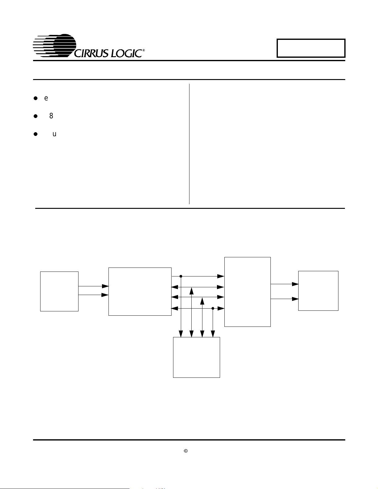
The CDB5340 evalua tion board is an excellent means
for quickly evaluating the CS5340 24-bit, stereo A/D converter. Evaluation requires a digital signal analyzer, an
analog signal source, and a power supply.
Also included is a CS8406 digital audio interface transmitter which generates S/PDIF, and EIAJ-340
compatible audio data. The digital audio data is available
via RCA phono and optical connectors.
ORDERING INFORMATION
CDB5340 Evaluation Board
ANALOG
INPUT
Cirrus Logic, Inc.
www.cirrus.com
CS5340
AES/EBU
TRANSMITTER
I/O FOR
CLOCKS
AND DATA
Copyright Cirrus Logic, Inc. 2003
(All Rights Reserved)
CS8406
S/PDIF
S/PDIF
OUTPUT
JUL ‘03
DS601DB1
1
Page 2

TABLE OF CONTENTS
C
F
T
I
C
ct
t
nt
i
le
s
y
C
ts
o
rk
r
s
c
t
d
A
al
a
d
f
w
a
C
-
E
E
I
-
I
Y
D
-
C
-
N
S
C
-
N
'
F
C
s
o
1. CDB5340 SYSTEM OVERVIEW .............................................................................................. 3
2. CS8406 DIGITAL AUDIO TRANSMITTER ...............................................................................3
3. INPUT/OUTPUT FOR CLOCKS AND DATA ...........................................................................3
4. POWER SUPPLY CIRCUITRY .................................................................................................3
5. GROUNDING AND POWER SUPPLY DECOUPLING ............................................................3
6. ANALOG INPUT FILTER .........................................................................................................3
LIST OF FIGURES
Figure 1. System Bl o ck Dia g ra m and Signal Flow.... ......... .......... ................... ......... ......... .......... ....5
Figure 2. Analog Audio Input...........................................................................................................6
Figure 3. CS5340 ............................................ ..... .. ..... .. ..... ....... ..... .. ..... .. ..... ....... ..... .. ..... .. ..............7
Figure 4. Level Shifters ...................................................................................................................8
Figure 5. CS8406 Digital Audio Interface........................................................................................9
Figure 6. Power Cir cu it........................ .......... ......... ................... .......... ......... ................... ..............10
Figure 7. Top Layer Silkscreen.....................................................................................................11
Figure 8. Top Layer..... ......... ................... .......... ......... .......... ......... ................... ......... ...................12
Figure 9. Botto m Layer....... ......... .......... ................... ......... .......... ......... .......... .................. ............13
LIST OF TABLES
Table 1. System Connec tions .......... ................... ......... .......... ......... ................... .......... ......... ......... 4
Table 2. CDB5340 Jumper and Switch Settings .................................. ....... ....... ..... ....... .. ............ ..4
CDB5340
ontacting Cirrus Logic Support
or all product questions and inquiries contact a Cirrus Logic Sales Representative.
o find one nearest you go to www.cirrus.com
MPORTANT NOTICE
irrus Logic, Inc. and its subsidiaries ("Cirrus") believe that the infor mation contained in this document is accurate and reliable. However, the inf ormation is subje
o change without not i ce and i s provided "AS IS" without warr anty of any ki nd ( expres s or impl ie d). Cust omers are advis ed to obt ain the latest version of releva
nformation to verify, before placing orders, that information being relied on is current and complete. All products are sold subject to the terms and conditions of sa
upplied at the time of order acknowledgment, including those pertaining to warranty, patent infringement, and limitation of liability. No responsibilit y is assumed b
irrus for the use of this information, including use of this information as the basis for manufacture or sale of any items, or for infringement of patents or other righ
f third parties. This document is the property of Cirrus and by furnishing this information, Cirrus grants no license, express or implied under any patents, mask wo
ights, copyrights, trademarks, trade secrets or other intellectual property rights. Cirrus owns the copyrights associated with the information contained herein and give
onsent for copies to be made of the information only for use within your organization with respect to Cirrus integrated circuits or other products of Cirrus. This consen
oes not extend to other copying such as copying for general distribution, advertising or promotional purposes, or for creating any wo rk f o r resale.
n export permit needs to be obtained from the competent authorities of the Japanese Government if any of the products or technologies described in this materi
nd controlled under the "Foreign Exchange and Foreign Trade Law" is to be exported or taken out of Japan. An export license and/ or quota needs to be obtaine
rom the competent authorities of the Chinese Government if any of the products or technologies described in this material is subject to the PRC Foreign Trade La
nd is to be exported or taken out of the PRC.
ERTAIN APPLICATIONS USING SEMICONDUCTOR PRODUCTS MAY INVOLVE POTENTIAL RISKS OF DEATH, PE RSONAL INJURY, OR SEVERE PROP
RTY OR ENVIRONMENTAL DAMAGE ("CRITICAL APPLICATIONS"). CIRRUS PRODUCTS ARE NOT DESIGNED, AUTHORIZED OR WARRANTED FOR US
N AIRCRAFT SYSTEMS, MILITARY APPLICATIONS, PRODUCTS SURGICALLY IMPLANTED INTO THE BODY, LIFE SUPPORT PRODUCTS OR OTHER CRIT
CAL APPLICATIONS (INCLUDING MEDICAL DEVICES, AIRCRAFT SYSTEMS OR COMPONENTS AND PERSONAL OR AUTOMOTIVE SAFETY OR SECURIT
EVICES). INCLUSION OF CIRRUS PRODUCTS IN SUCH APPLICATIONS IS UNDERSTOOD TO BE FULLY AT THE CUSTOMER'S RISK AND CIRRUS DIS
LAIMS AND MAKES NO WARRANTY, EXP RESS, STATUT ORY OR IMPLI ED, INCLUDING THE IMPL IED WARRANTI ES OF MERCHANTABIL IT Y AND FI T
ESS FOR PARTICULAR PURPOSE, WITH REGARD TO ANY CIRRUS PRODUCT THAT IS USED IN SUCH A MANNER. IF THE CUSTOMER OR CUSTOMER'
USTOMER USES OR PERMITS THE USE OF CIRRUS PRODUCTS IN CRITICAL APPLICATIONS, CUSTOMER AGREES, BY SUCH USE, TO FULLY INDEM
IFY CIRRUS, ITS OFFICERS, DIRECTORS, EMPLOYEES, DISTRIBUTORS AND OTHER AGENTS FROM ANY AND ALL LIABILITY, INCLUDING ATTORNEYS
EES AND COSTS, THAT MAY RESULT FROM OR ARISE IN CONNECTION WITH THESE USES.
irrus Logic, Cirrus, and the Cirrus Logic logo designs are trademarks of Cirrus Logic, Inc. All other brand and product names in this document may be trademark
r service marks of their respective owners.
2 DS601DB1
Page 3

CDB5340
1. CDB5340 SYSTEM OVERVIEW
The CDB5340 evaluation board is an excellent means of quickly evaluating the CS5340. The
CS8406 digital audio i nte rface tr ansmitt er pro vi des an easy inte rface to digi tal audio si gna l analyzers including the majority of digital audio test equipment.
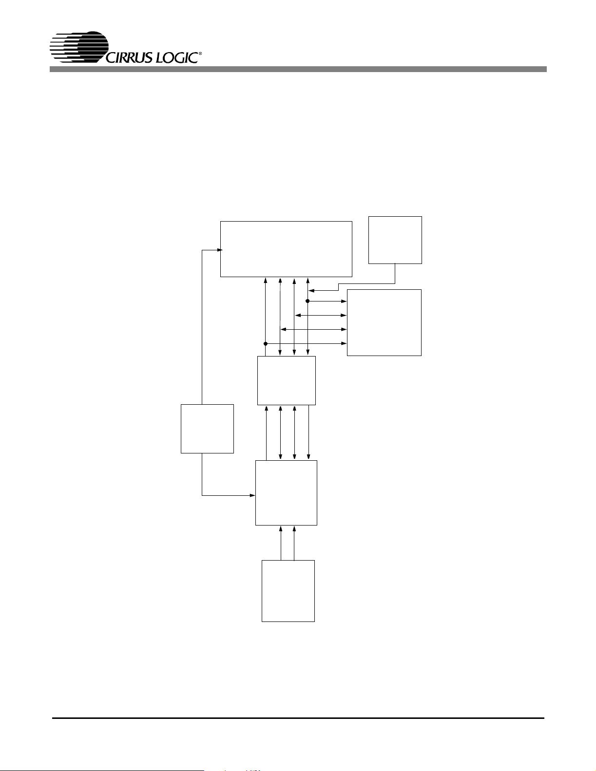
The CDB5340 schematic has been partitioned into 5 schematics shown in Figure 2 through
Figure 6. Each partitioned schematic is represented in the system diagram shown in Figure 1.
Notice that the system diagram also includes the interconnections between the
partitioned schematics.
2. CS8406 DIGITAL AUDIO TRANSMITTER
The system generate s and enc odes stan dard S/PD IF data usin g a CS8 406 Digita l Audio Tra nsmitter (see Figure 5). The outputs of the CS8406 are RS422 compatible differential line drivers.
The CS8406 supports both Lef t Justified and I2S data formats, as determin ed by the DIP switch,
S2. A description of the CS8406 is included in the CS8406 datasheet.
3. INPUT/OUTPUT FOR CLOCKS AND DATA
The evaluation board has been designed to allow interfacing to external systems via the 10-pin
header, J11. The schematic for the clock/data input/output is shown in Figure 4.
The CDB5340 allows some flexibility as to the generation of the clocks. When the CS5340 and
CS8406 are in slave mode, the SCLK and LRCK must be provided via the header, J11. MCLK
can be gene rated from t he on-boa rd oscillator, Y 1 or pr ovided via the header, J11 as determ ined
by the DIP switch, S2. The on- boar d oscillator is sockete d to allow ot her fr eque ncy oscillators to
be used. Please note that the on-board oscillator must be removed if an external MCLK is provided through header J11.
4. POWER SUPPLY CIRCUITRY
Power is supplied to the evaluation board by four binding posts (VA/VD, VL, GND, +5V),
see Figure 6. The VA/VD input supplies the VA and VD pins of the CS5340. VL supplies power
to the VL pin of the CS5340 and to the level shifter circuits. Th e +5 V input suppl ies power to the
digital circuitry and the input amplifiers.
5. GROUNDING AND POWER SUPPLY DECOUPLING
The CS5340 requires car eful atte ntion to power supply and grounding arr angements to optimize
performance. Figure 3 details the power distribution used on this board. The decoupling capacitors are located as close to the CS5340 as possible. Extensive use of ground plane fill in the
evaluation board yields large reductions in radiated noise.
6. ANALOG INPUT FILTER
The CDB5340 implements a single-ended analog input buffer, as shown in Figure 2. Note that
there is no attenuation or gain associated with the input buffer.
DS601DB1 3
Page 4

CDB5340
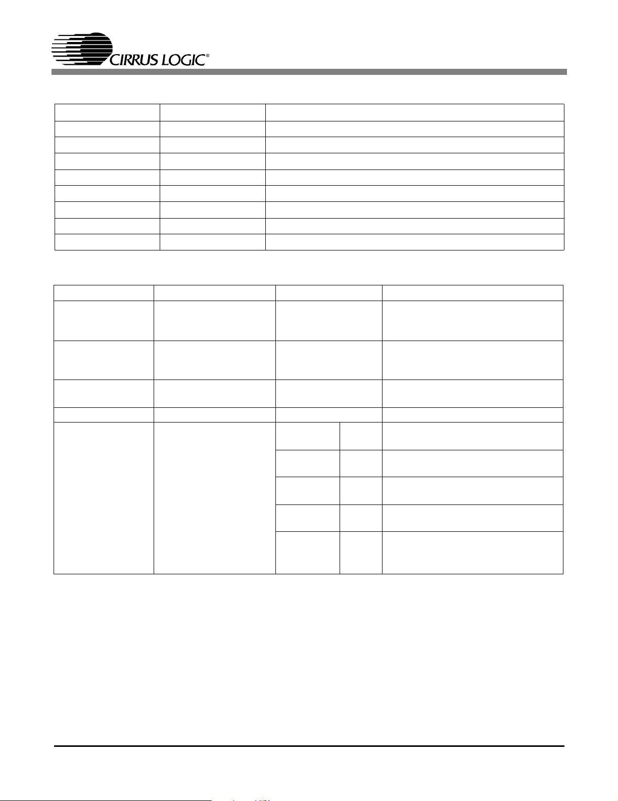
CONNECTOR INPUT/OUTPUT SIGNAL PRESENT
VA/VD Input +3.3V to +5V power for the CS5340
VL Input +2.5V to +5V power for the CS5340
GND Input Ground connection from power supply
+5V Input + 5 Volt power
AINL Input Analog input left channel
AINR Input Analog input right channel
Optical Output Output Digital audio output
Coax Output Output Digital audio output
Table 1. System Connections
JUMPER/SWITCH PURPOSE POSITION FUNCTION SELECTED
J5 VA/VD Power Source ADJ
*+3.3V
+5V
J6 VL Power Source ADJ
*+3.3V
+5V
J11 Input/Output for
--
clocks/data
S1 Reset for the CDB5340 - S2 CDB5340 Configuration M1/M0 Open
*ClosedHiLow
SCLK/LRCK Open
*Closed
MCLK Open
*Closed
8406 Open
*Closed
DIF Open
*Closed
Power from the Binding Post (J1)
Power from the +3.3V Regulator
Power from the +5V Supply
Power from the Binding Post (J2)
Power from the +3.3V Regulator
Power from the +5V Supply
Header J11 is an input for clocks.
Header J11 is an output for clocks.
Header J11 is an input for MCLK.
Header J11 is an output for MCLK.
CS8406 in Master mode
CS8406 in Slave mode
Digital interface format set to I
Digital interface format set to
Left Jus tified
2
S
Table 2. CDB5340 Jumper and Switch Settings
* denotes default factory settings
4 DS601DB1
Page 5

CDB5340
R
O
T
A
4
L
L
I
G
I
C
F
S
AUDIO
CS8406
DIGITAL
FIG 5
INTERFACE
CRYSTAL
O
RESET
CIRCUIT
FIG 6
LEVEL
SHIFTER
CS5340
T
U
P
N
I
G
O
L
A
N
A
I/O FOR
FIG 4
3
G
I
F
FIG 4
CLOCKS
AND DATA
Figure 1. System Block Diagram and Signal Flow
2
G
I
F
DS601DB1 5
Page 6

CDB5340
Figure 2. Anal og Audio Input
6 DS601DB1
Page 7

CDB5340
CS5340 Data Modes
CS5340-CZ
Figure 3. CS5340
DS601DB1 7
Page 8

CDB5340
Figure 4. Leve l Sh ifte rs
8 DS601DB1
Page 9

CDB5340
Figure 5. CS8406 Digital Audio Interface
DS601DB1 9
Page 10

CDB5340
Figure 6. Power Circuit
10 DS601DB1
Page 11

CDB5340
C
C
0
CS5340 Data Modes
CDB5340
DB5340
Figure 7. Top Layer Silkscree n
S534
CDB5340
DS601DB1 11
Page 12

CDB5340
Figure 8. Top Layer
12 DS601DB1
Page 13

CDB5340
Figure 9. Bottom Layer
DS601DB1 13
Page 14

CDB4398
18
 Loading...