Page 1
CDB5330A
CDB5331A
Evaluation Board for CS5330A / CS5331A
Features
Demonstrates recommended layout
•
and grounding arrangements
CS8402A Generates AES/EBU, S/PDIF,
•
& EIAJ-340 Compatible Digital Audio
Buffered Serial Output Interface
•
Digital and Analog Patch Areas
•
On-board or externally supplied system
•
timing
General Description
The CDB5330A/31A evaluation board is an excellent
means for quickly evaluating the CS5330A/31A 18-bit,
stereo A/D converter. Evaluation requires a digital
signal processor, a low distortion analog signal
source and a power supply. Analog inputs are provided via RCA connectors for both channels.
Also included is a CS8402A digital audio interface
transmitter which generates AES/EBU, S/PDIF, and
EIAJ-340 compatible audio data. The digital audio data
is available via RCA phono, and optical connectors.
The evaluation board may also be configured to accept
external timing signals for operation in a user application during system development.
ORDERING INFORMATION: CDB5330A, CDB5331A
Analog
Filter
Cirrus Logic, Inc.
Crystal Se micond ucto r Prod uct Divisi on
P.O. Box 17847, Austin, TX 78760
(512) 445-7222 FAX: (512) 445-7581
http://www.crystal.com
CS5330A/31A
I/OforClocks
andData
Copyri ght Cirrus Logic, Inc. 1997
CS8402A
Digital
Audio
Interface
(All Rights Reserved)
Digital
Audio
Output
OCT ’97
DS138DB2
17
Page 2

CDB5330A / CDB5331A
CDB5330A/31A System Overview
The CDB5330A/31A evaluation board is an excellent means of quickly evaluating the
CS5330A/31A. The CS8402A digital audio interface transmitter provides an easy interface to
digital audio signal processors, including the majority of digital audio test equipment. The
evaluation board has been designed to accept an
analog input, and provide a digital output that is
either optical or coax. The evaluation board also
allows the user to supply clocks and data
through a 10-pin header for system development.
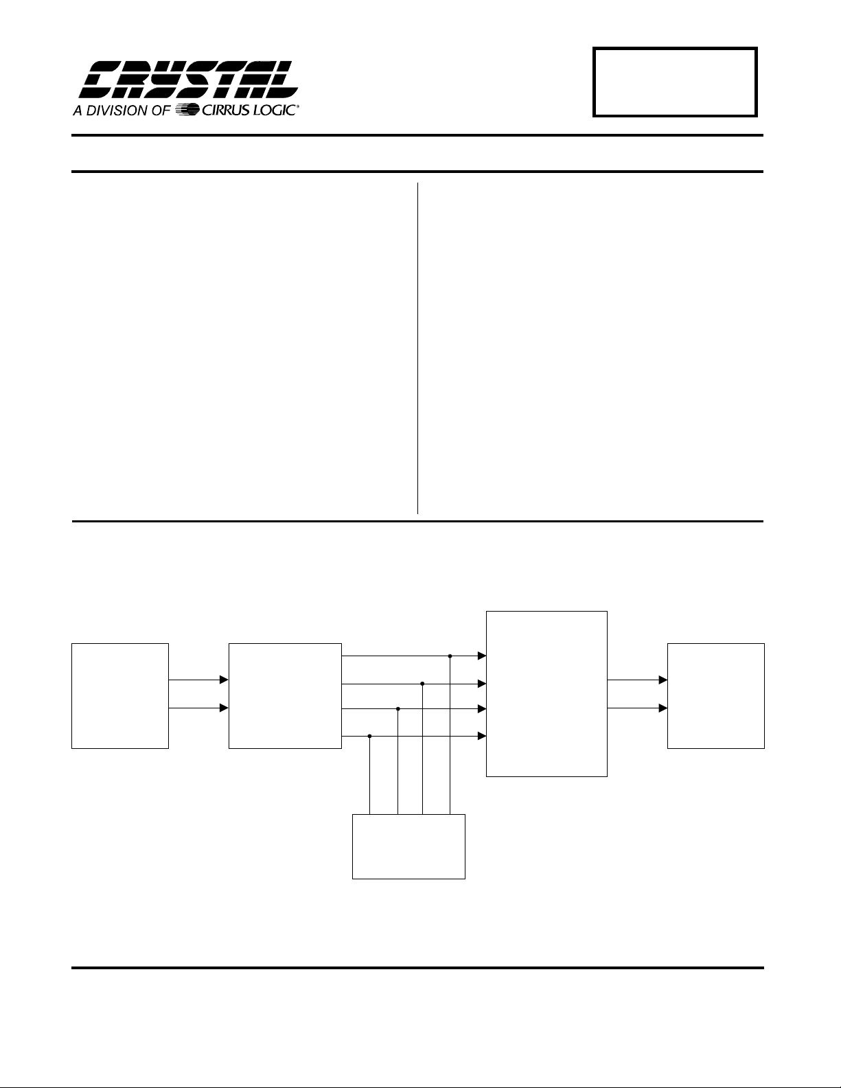
The CDB5330A/31A schematic has been partitioned into 5 schematics shown in Figures 2
through 6. Each partitioned schematic is represented in the system diagram shown in Figure 1.
Notice that the the system diagram also includes
the interconnections between the partitioned
schematics.
CS5330A/31A Analog to Digital Converter
A description of the CS5330A/31A is included
in the CS5330A/31A data sheet.
CS8402A Data Format
The CS8402A data format can be set with jumpers M0, M1, and M2. These formats are shown
in the CS8402A datasheet found in the 1994
Crystal Semiconductor Audio Data Book. The
format selected must be compatible with the corresponding data format of the CS5330A/31A
shown in Figures 2 and 3 of the CS5330A/31A
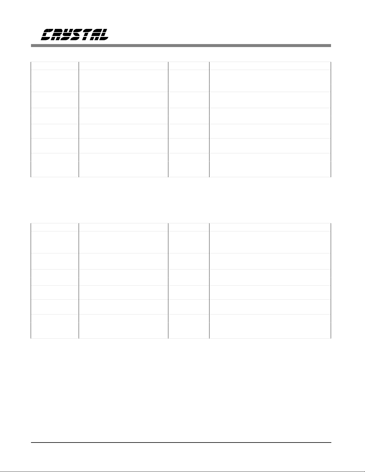
datasheet. The default settings for M0-M2 on the
evaluation board are given in Tables 2 and 3.
The compatible data formats for the CS8402A
and CS5330A/31A are:
CS8402A format 1;CS5330A
CS8402A format 4;CS5331A
Analog input buffer
The recommended input filter required for the
CS5330A/31A has been combined with a unity
gain input buffer (see Figure 2). The analog input filter uses a Motorola MC33202 single
supply, dual op-amp.
Power Supply Circuitry
CS8402A Digital Audio Interface
Power is supplied to the evaluation board by two
Figure 4 shows the CS8402A circuitry which
implements AES/EBU, S/PDIF and EIAJ CP340 digital audio interface standards. The
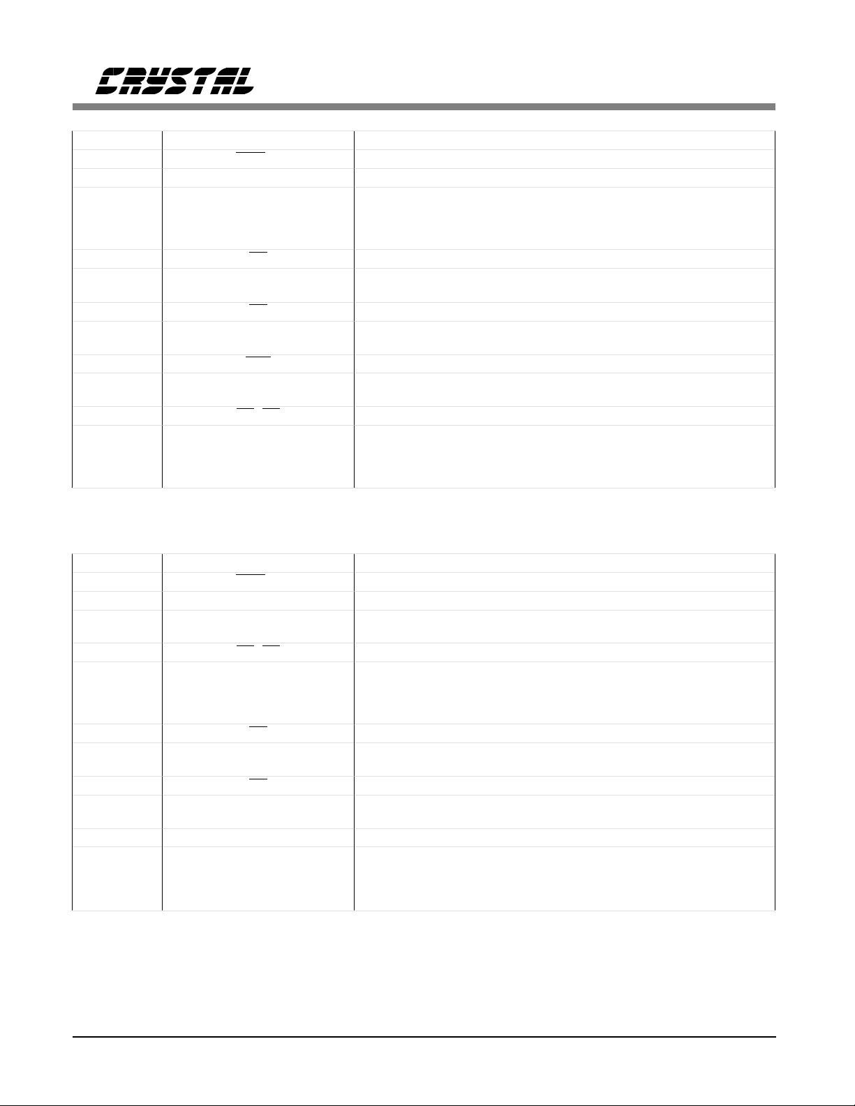
CS8402A circuit is hardware configured for consumer mode. SW2 provides 8 DIP switches to
binding posts (GND, +5V), Figure 6. The +5V
input supplies power to the +5 Volt digital circuitry (VD+), and the +5V analog circuitry
(VA+). The analog supply is derived from the
+5V binding post through a ferrite bead.
select various modes and bits for the CS8402A,
Tables 4-5. See the CS8401A/CS8402A data
Input/Output for Clocks and Data
sheet for detailed information on the operation of
the CS8402A and the digital audio standards.
The operation of the CS8402A and a discussion
of the digital audio interface are included in the
1994 Crystal Semiconductor Audio Data Book.
The evaluation board has been designed to allow
the interface to external systems via the 10-pin
CLOCK I/O header, HDR2. This header allows
the evaluation board to accept externally generated clocks. The schematic for the clock/data I/O
is shown in Figure 5. The 74HC243 transceiver
functions as an I/O buffer where the MASTER/SLAVE jumper determines if the
transceiver operates as a trans mitter or receiver.
18 DS138DB2
Page 3
CDB5330A / CDB5331A
The transceiver operates as a tr ansmitter with the
MASTER/SLAVE jumper in the MAST ER position. LRCK, SDATA, and SCLK from the
CS5330A/31A will be available on HDR2.
HDR22 must be in the 0 position and HDR23
must be in the 1 position for MCLK to be an
output and to avoid bus contention on MCLK.
The transceiver operates as a receiver with the
MASTER/SLAVE jumper in the SLAVE position. LRCK and SCLK on HDR2 become inputs.
However, the recommended mode of operation is
to generate MCLK on the evaluation board with
HDR23 in the 0 position and HDR22 in the 1
position. These default settings allow MCLK to
be an output, with LRCK and SCLK as inputs.
MCLK is always an output from the evaluation
board.
Grounding and Power Supply Decoupling
The CS5330A/31A requires careful attention to
power supply and grounding arrangements to optimize performance. Figure 2 shows the
recommended power arrangements. The
CS5330A/31A is positioned over the analog
ground plane, near the digital/analog ground
plane split, to minimize the distance that the
clocks travel. The series resistors are present on
the clock lines to reduce the effects of transient
currents when driving a capacitive load in master
mode, and reduce clock overshoot when applying external clocks to the CS5330A/31A in slave
mode.
This layout technique is used to minimize digital
noise and to insure proper power supply matching/sequencing. The decoupling capacitors are
located as close to the CS5330A/31A as possible. Extensive use of ground plane fill on both
the analog and digital sections of the evaluation
board yield large reductions in radiated noise effects.
CONNECTOR INPUT/OUTPUT SIGNAL PRESENT
+5V input
GND input ground connection from power supply
AINL input left channel analog input
AINR input right channel analog input
MCLK, SCLK, LRCK,
SDATA
Digital Output output digital audio interface output via coax
Optical Output output digital audio interface output via optical
DS138DB2 19
input/output I/O for master, serial, left/righ t clocks, and serial DATA
Table 1. System Connections
(VD+) for CS8402A and digital section
(VA+) for CS5330A/31A and Analog input filter op-amp
Page 4
CDB5330A / CDB5331A
JUMPER PURPOSE POSITION FUNCTION SELECTED
HDR1
HDR10
HDR9
HDR22
HDR23
HDR6
HDR5 (M2)
HDR4 (M1) *Low
HDR3 (M0) *High
* Default setting from factory
CS5330A/31A SCLK
Selection for CS8402A
Master/Slave Mode
Selection
Selects source of system
clocks
Clock I/O
Selects 256× or
512× MCLK for CS8402A
CS8402A mode select
Table 2. CDB5330A Jumper Selectable Options
*5330A CS5330A Selected
5331A CS5331A Selected
*High
Low
*High MASTER Mode (5330A Clocks)
Low SLAVE Mode (External Clocks)
*0
*1
*256
512
*Low
MASTER Mode
SLAVE Mode
Input/Output for Clocks and Data
See
section of text
See CS8402A data sheet for details
See CS8402A data sheet
for details
JUMPER PURPOSE POSITION FUNCTION SELECTED
HDR1
HDR10
HDR9
HDR22
HDR23
HDR6
HDR5 (M2)
HDR4 (M1) *Low
HDR3 (M0) *Low
* Default setting from factory
CS5330A/31A SCLK
Selection for CS8402A
Master/Slave Mode
Selection
Selects source of system
clocks
Clock I/O
Selects 256× or
512× MCLK for CS8402A
CS8402A mode select
Table 3. CDB5331A Jumper Selectable Options
5330A CS5330A Selected
*5331A CS5331A Selected
*High
Low
*High MASTER Mode (5331A Clocks)
Low SLAVE Mode (External Clocks)
*0
*1
*256
512
*High
MASTER Mode
SLAVE Mode
Input/Output for Clocks and Data
See
section of text
See CS8402A data sheet for details
See CS8402A data sheet
for details
20 DS138DB2
Page 5
Switch# 0=Closed, 1=Open Comment
3
1,4 FC1, FC0 C24,C25,C26,C27 - Sample Frequency
2
5
6
8,7
* Default setting from factory
PRO=0 Consumer Mode C0=0
0 0
*0 1
1 0
1 1
C3 C3,C4,C5 - Emphasis (1 of 3 bits)
*1
0
C2 C2 - Copy/Copyright
1
*0
C15 C15 - Generation Status
1
*0
C8, C9 C8-C14 - Category Co de (2 of 7 b its)
1 1
1 0
0 1
*0 0
0000 - 44.1 kHz
0100 - 48 kHz
1100 - 32 kHz
0000 - 44.1 kHz, CD Mode
000 - None
100 - 50/15 µs
0 - Copy Inhibited/Copyright Asserted
1 - Copy Permitted/Copyright No t Asserted
0 - Definition is based on category code.
1 - See CS8402A Data Sheet, App. A
0000000 - General
0100000 - PCM encoder/decoder
1000000 - Compact Disk - CD
1100000 - Digital Audio Tape - DAT
CDB5330A / CDB5331A
Table 4. CS8402A Switch Definitions - Consumer Mode
Switch# 0=Closed, 1=Open Comment
3
1 CRE Local Sample Address Coun ter & Reliability Fla gs
default
2,5
default
4
default
6
default
8,7 EM1, EM0 C2,C3,C4 - Emphasis (2 of 3 bits)
default
PRO=0 Professional Mode C0=1(default)
0
1
C6, C7 C6,C7 - Sample Frequency
1 1
1 0
0 1
0 0
C1 C1 - Audio
1
0
C9 C8,C9,C10,C11 - Channel Mode (1 of 4 bits)
1
0
1 1
1 0
0 1
0 0
Disabled
Internally Generated
00 - Not Indicated - Default to 48 kHz
01 - 48 kHz
10 - 44.1 kHz
11 - 32 kHz
0 - Normal Audio
1 - Non-Audio
0000 - Not indicated - Default to 2-channel
0100 - Stereophonic
000 - Not Indicated - default to none
100 - No emphasis
110 - 50/15 µs
111 - CCITT J.17
Table 5. CS8402A Switch Definitions - Professional Mode
DS138DB2 21
Page 6

CDB5330A / CDB5331A
Figure 1. System Block Diagram and Signal Flow
22 DS138DB2
Page 7

DS138DB2 23
Figure 2. CS5330A/31A and Connections
CDB5330A / CDB5331A
Page 8

CDB5330A / CDB5331A
Figure 3. MCLK Generation and Power Down
24 DS138DB2
Page 9

DS138DB2 25
Figure 4. CS8402A Digital Audio Transmitter Connections
Optional Toshi ba P art T OTX123 avail able thro ugh In sigh t El ectro nics
Schott Corp. Transformer Part 121960-602 available through Schott Corp., Wayzata, MN.
CDB5330A / CDB5331A
Page 10

CDB5330A / CDB5331A
Figure 5. I/O Interface for Clocks and D ata
Figure 6. Power Supply
26 DS138DB2
Page 11

CDB5330A / CDB5331A
Figure 7. CDB5330A/31A Component Side Silkscreen
DS138DB2 27
Page 12

CDB5330A / CDB5331A
Figure 8. CDB5330A/31A Component Side (top)
28 DS138DB2
Page 13

CDB5330A / CDB5331A
Figure 9. CDB5330A/31A Solder Side (bottom)
DS138DB2 29
Page 14

 Loading...