Page 1

CDB4954A/55A
Evaluation Board for CS4954/55
Features
l Demonstrates recommended layout and
grounding practices
l Supports both parallel and serial digital
video input
l On-board test pattern generation
l Supports NTSC/PAL video formats
l 3.3 V or 5 V operation
l Composite, S-Video, and RGB outputs
l Supports Standalone mode via onboard
DIP switch
l RS232 interface with PC
l Single 6-9 V external DC power supply
l Additional op-amps with open pads for
prototyping additional filters
I
D
B
9
PC SERIAL
INTERFACE
Reset
Switch
TXD
RXD
Reset
6.5 - 10VDC
RS-232
Interface
POWER
INLET
MPU
PROGRAM
HEADER
RESET-
PROG
TX
RX
Regulator
Regulator
1
2
3
4
5
6
7
8
Motorola 908
Microcontroller
SDL
SDA
+3.3V
3.3V
or
+5V
+5V
ISP
OPEN
A/D7:0
RESET
245
BUFFER
Hdr 16PIN
SDA_O
SCL
Description
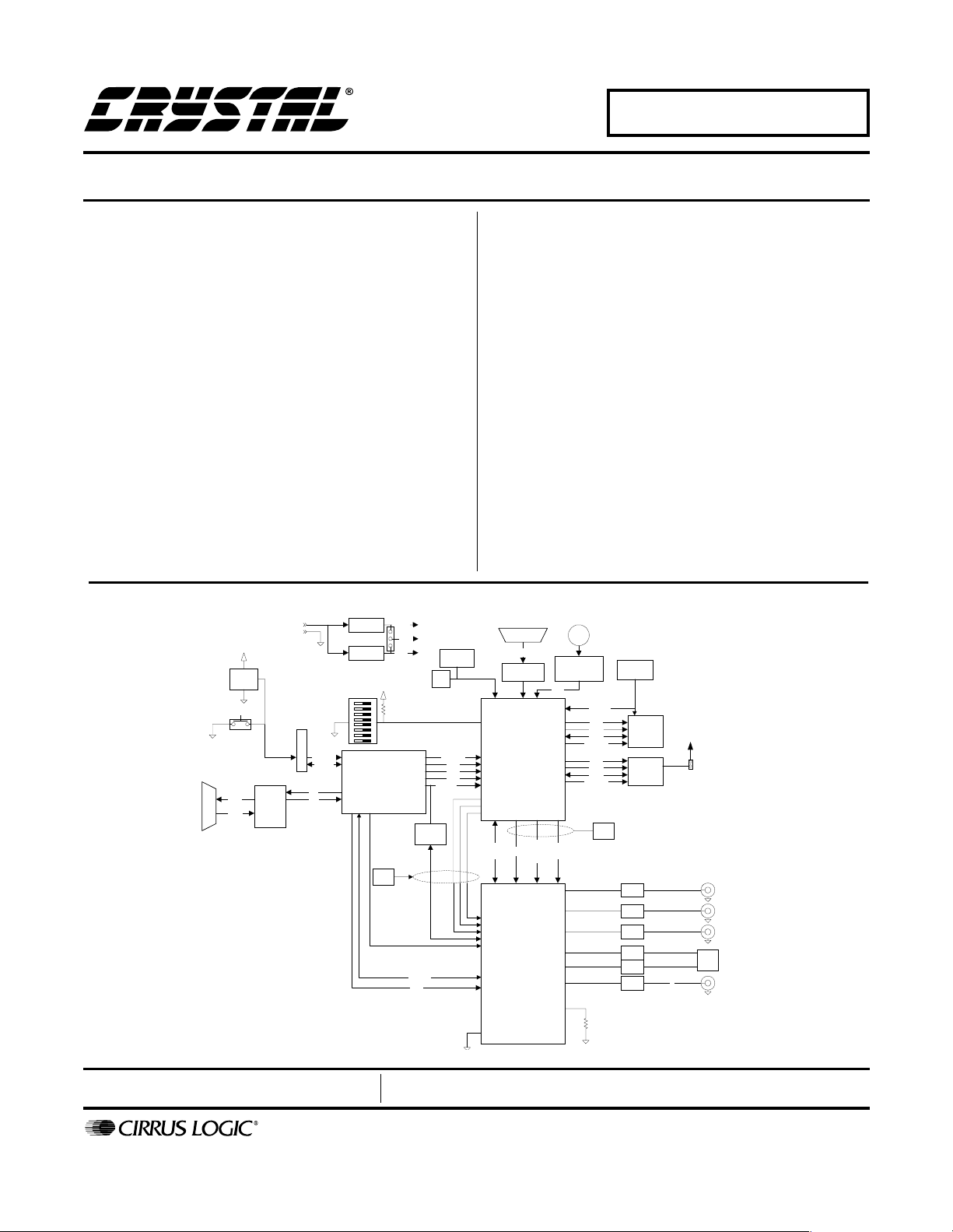
The CDB4954A/55A board allows fast evaluation of the
features of the CS4954 digital video encoders. The
board may also be configured to accept external TTL
level timing and data signals for use during system
development.
Also, to simplify the demonstration of the features of the
CS4954, the CDB4954A/55A is equipped with an onboard microcontroller and pre-programmed FLASH
memory to facilitate configuration and evaluation of
CS4954 digital video encoder.
ORDERING INFORMATION
CDB4954A Evaluation Board
CDB4955A Evaluation Board
CCIR 656 SERIAL/ PARALELL
INPUTS
656
DATA
/8
HS,VS,
CVBS
656
FIELD
BNC
SMPTE-259M
Interface
R
G
B
Y
C
54MHZ
CTL
Addr
Data
RESET-
CTL
Addr
Data
RESET-
Hdr 16PIN
OSC
SDRAM
Flash
SELECTABLE
HI/LOW
IMPEDANCE
FILTERS
OUT
FILT
OUT
FILT
OUT
FILT
OUT
FILT
OUT
FILT
OUT
FILT
u
PROGRAMMING
ENABLE
JUMPER
CONNECTORS
CONN.
CONNECTOR
RCA
DIN4
RCA
PLD
EEPROM
RESET-
ALE
WRRD-
TTX
/2
TTXD,
TTXRQ
ADDR
RDWRDAT<7..0>
RST-
SDA
SCL
DB25
656_IN
ECL
RECEIVER
FPGA
27MHz
CS4954
the
Preliminary Product Information
P.O. Box 17847, Austin, Texas 78760
(512) 445 7222 FAX: (512) 445 7581
http://www.cirrus.com
4K
TEST
1%
This document contains information for a new product.
Cirrus Logic reserves the right to modify this product without notice.
Copyright Cirrus Logic, Inc. 2001
(All Rights Reserved)
DS278DB2
MAY ‘01
1
Page 2

TABLE OF CONTENTS
1. CDB4954A/55A SYSTEM OVERVIEW .................................................................................... 4
2. SETUP ACTIVITIES .................................................................................................................. 4
2.1 DIP Switch Options ............................................................................................................ 4
2.2 Control Port Software ......................................................................................................... 4
2.2.1 Changing a CS4954/5 or FPGA Register ............................................................. 4
2.2.2 Actions Menu ........................................................................................................ 5
2.2.2.1 Convert to CCIR656 File Option ........................................................... 5
2.2.2.2 Video Input Source Option .................................................................... 6
2.2.2.3 Download a CCIR656 File to SDRAM and Display Option ................... 6
2.2.2.4 Download a CCIR656 File to Flash Option ........................................... 6
2.2.2.5 Display Video from Flash Option ........................................................... 6
2.2.2.6 Display Test Patterns Option ................................................................ 6
3. COMMAND LINE PARAMETERS ............................................................................................ 6
4. 3.3 V OR 5 V INTERFACE ........................................................................................................ 6
5. DIGITAL VIDEO INTERFACE .................................................................................................. 6
6. ANALOG OUTPUT ................................................................................................................... 6
7. OUTPUT FILTERS .................................................................................................................... 6
LIST OF FIGURES
CDB4954A/55A
Figure 1. CDB4954A/55A Evaluation Board Interface .................................................................... 5
Figure 2. Register Edit Box ............................................................................................................. 5
Figure 3. 300 Ω Filters..................................................................................................................... 7
Figure 4. 75 Ω Filters....................................................................................................................... 7
Figure 5. Digital Video Input ............................................................................................................ 9
Figure 6. FPGA ............................................................................................................................. 10
Figure 7. CS4954/5 ....................................................................................................................... 11
Figure 8. Microprocessor............................................................................................................... 12
Figure 9. Video Output Filters ....................................................................................................... 13
Figure 10. Power/RS232 Interface ................................................................................................14
Figure 11. Silkscreen Top ............................................................................................................. 15
Figure 12. Top Side ....................................................................................................................... 16
Figure 13. Power Layer ................................................................................................................. 17
Figure 14. Ground Layer ............................................................................................................... 18
Figure 15. Bottom Side.................................................................................................................. 19
Contacting Cirrus Logic Support
For a complete listing of Direct Sales, Distributor, and Sales Representative contacts, visit the Cirrus Logic web site at:
http://www.cirrus.com/corporate/contacts/
Microsoft, Windows 95, Windows 98, Windows 2000, and Windows NT are registered trademarks of Micosoft Corporation. IBM is a registered trademark of
International Business Machines, Inc. Macrovision is a registered trademark of Macrovision Corporation.
Preliminary product information describes products which are in production, but for which full characterization data is not yet available. Advance product information describes products which are in development and subject to development changes. Cirrus Logic, Inc. has made best efforts to ensure that the information
contained in this document is accurate and reliable. However, the information is subject to change without notice and is provided “AS IS” without warranty of
any kind (express or implied). No responsibility is assumed by Cirrus Logic, Inc. for the use of this information, nor for infringements of patents or other rights
of third parties. This document is the property of Cirrus Logic, Inc. and implies no license under patents, copyrights, trademarks, or trade secrets. No part of
this publication may be copied, reproduced, stored in a retrieval system, or transmitted, in any form or by any means (electronic, mechanical, photographic, or
otherwise) without the prior written consent of Cirrus Logic, Inc. Items from any Cirrus Logic website or disk may be printed for use by the user. However, no
part of the printout or electronic files may be copied, reproduced, stored in a retrieval system, or transmitted, in any form or by any means (electronic, mechanical,
photographic, or otherwise) without the prior written consent of Cirrus Logic, Inc. The names of products of Cirrus Logic, Inc. or other vendors and suppliers
appearing in this document may be trademarks or service marks of their respective owners which may be registered in some jurisdictions. A list of Cirrus Logic,
Inc. trademarks and service marks can be found at http://www.cirrus.com.
2
Page 3

CDB4954A/55A
LIST OF TABLES
Table 1. System Connections................................................................................................................ 7
Table 2. CBD4954 Jumper/Switch Settings........................................................................................... 7
Table 3. DIP Switch Settings ................................................................................................................. 8
3
Page 4

CDB4954A/55A
1. CDB4954A/55A SYSTEM OVERVIEW
The CDB4954A/55A Evaluation Board allows the
CS4954/55 NTSC/PAL Digital Video Encoder ICs
from Cirrus Logic to be evaluated with a variety of
internal and external video signals. DIP switches on
the evaluation board allow external serial or parallel
video to drive the CS4954/55, display test patterns
contained in the evaluation board’s control FPGA,
and display NTSC images stored in FLASH. When
the CDB4954A/55A (Microsoft Windows95®,
Windows 98®, Windows NT®, and Windows
2000® compatible) software is used, bitmaps up to
720x480 pixels may be converted to CCIR656 PAL
or NTSC files, downloaded to SDRAM on the evaluation board and played from SDRAM through the
CS4954/55. In addition, NTSC CCIR656 files can
be stored to FLASH memory on the evaluation
board for later play back. The CDB4954A/55A
board supports Composite, RGB and S-Video outputs simultaneously.
The CDB4954A/55A has been partitioned into 6
schematics shown in Figure 5, Figure 6, Figure 7,
Figure 8, Figure 9, and Figure 10. Notice that the
partitioned schematics show the interconnections
between the pages.
2.1 DIP Switch Options
If you use the CDB4954A/55A Evaluation Board
without a PC (i.e. in the standalone mode), use the
followings to set up the board using the 8 position
dip switch. The dip switch positions are marked 1-
8. The individual switches select these functions:
Switches 1-4 select different operating modes. (Refer to Table 3 on page 8 for more information.)
Switch 5 - Not Used
Switch 6 - PAL/NTSC data format.
Switch 7 - Pedestal Offset ON/OFF.
Switch 8 - Clipping Input Signals ON/OFF.
2.2 Control Port Software
The CDB4954A/55A is shipped with Microsoft
Windows® based software for interfacing with the
CS4954/55 via the DB9 connector, J26. This software allows the user to have complete access to the
control registers of the CS4954/55, as well as the
ability to access some features of the on-board FPGA. A comprehensive online Help is included.
2.2.1 Changing a CS4954/5 or FPGA Register
®
2. SETUP ACTIVITIES
Setup of the CDB4954A/55A is straightforward.
DC Power is supplied to the board either via the
supplied “wall wart” style power supply or by using the binding posts on the board (but not both!)
When the board is powered, the Power In LED
(D6) will illuminate. If you're planning to use the
supplied software, you will need to copy the files
on the distribution disk shipped with the evaluation
board to your hard disk drive. You should use the
supplied 9-pin serial cable to connect your IBM
PC (or compatible) to the 9-pin D-Sub connector
(labeled J6, RS-232) on the CDB4954A/55A.
4
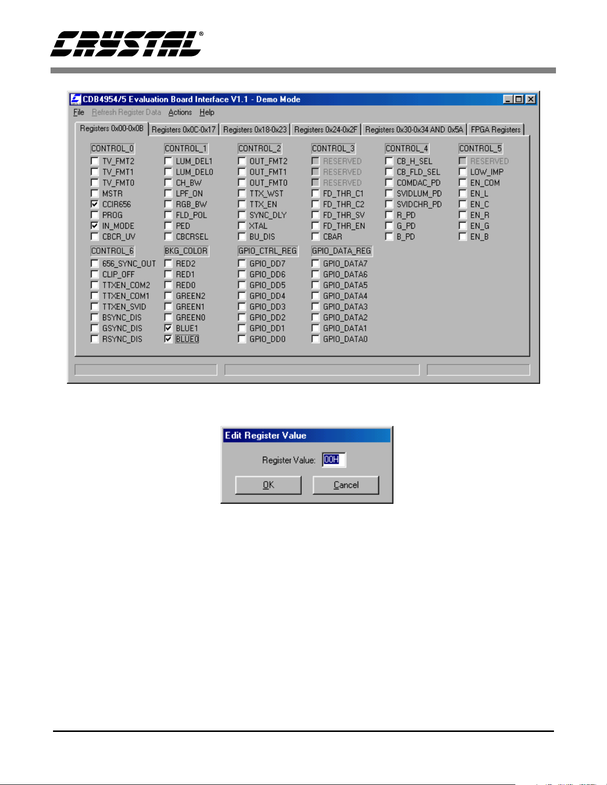
There are two ways to change the values of either
CS4954/55 or FPGA registers. When a register
check box is checked, the corresponding register
bit is set to a “1”. When unchecked, the bit is set to
“0”. The first approach, shown on Figure 1 on page
5, is to check or uncheck particular bit values in the
desired register. For example, in Figure 1, the
CONTROL_0 configuration register of the
CS4954/55 is set for CCIR656 mode (CCIR656
check box checked) and for video input from
V[7:0] (IN_MODE check box checked). In addi-
®
tion, the background color generated by the
CS4954/55 is set to blue (BLUE1 and BLUE0
check boxes are checked). The second approach is
to click the register label above any set of register
check boxes. This brings up a dialog which is
Page 5

CDB4954A/55A
Figure 1. CDB4954A/55A Evaluation Board Interface
Figure 2. Register Edit Box
shown in Figure 2. You can directly enter the hex
value for all bits in the register and click the OK
button. This will set all bits at once. The new value
will be reflected in the pattern of checks in the register check boxes and immediately downloaded to
either the CS4954/55 or the FPGA.
2.2.2 Actions Menu
If you use the CDB4954A/55A Evaluation Board
with a PC, the Action Menu will allow you to convert bitmaps of up to 720x480 pixels to CCIR656
PAL or NTSC files. These converted files can then
be downloaded to the FLASH on the evaluation
board for storage and later replay, or downloaded
directly to SDRAM for immediate playing.
2.2.2.1 Convert to CCIR656 File Option
This option converts a bitmap image (“.bmp” file
extension) of up to 720x480 into a CCIR656 NTSC
(“.nts” file extension) or PAL (“.pal” file extension) file. This step is necessary before attempting
to download either a NTSC or PAL image to
SDRAM and displaying it. It is also necessary before saving an NTSC or PAL file to FLASH.
5
Page 6

CDB4954A/55A
2.2.2.2 Video Input Source Option
This option selects the video source which will
serve as input for the CS4954/55. Internal Video
means all video content which is supplied by the
FPGA. External parallel inputs use J4, the 25 pin
D-Sub connector. External serial inputs use J19,
the right angle BNC connector.
2.2.2.3 Download a CCIR656 File to SDRAM and Display Option
This option downloads a previously converted bitmap file to SDRAM on the evaluation board and
displays it on the video outputs. Either a NTSC or
a PAL format file may be downloaded and displayed, but the monitor used must be compatible
with the downloaded file format to display correctly.
2.2.2.4 Download a CCIR656 File to Flash Option
This option downloads and stores a previously converted bitmap file to a block of on board Flash
memory. FLASH block 1 is contains the Cirrus
logo screen in NTSC format, while FLASH block
2 contains the Cirrus logo screen in PAL format.
2.2.2.5 Display Video from Flash Option
This option displays video from one of the 3
FLASH blocks.
2.2.2.6 Display Test Patterns Option
This option displays one of the eight test patterns
generated by the control FPGA. These patterns are
color bars, luma bars, step, aqua screen, luma ramp
(1 bit/2 pixel ramp rate), luma ramp (1bit/pixel),
luma ramp (2bits/pixel), and luma ramp (4bits/pixel).
3. COMMAND LINE PARAMETERS
There are two valid command line parameters
which can be used to modify the action of the program.
-f: This parameter shows the FPGA Register Values tab. This allows FPGA registers to be manipulated directly. Note that the FPGA Register is NOT
part of the CS4954/55.
-m: This parameter shows the Macrovision
isters tabs if a CS4955 is in place on the
CDB4954A/55A Evaluation Board. If a CS4954 is
in place on the board, the Macrovision Registers
tabs are not shown (since the CS4954 doesn’t have
Macrovision support) whether or not the "-m" command line parameter is included.
®
Reg-
4. 3.3 V OR 5 V INTERFACE
The CS4954 allows either 3.3 V or 5 V operation. The
CDB4954A/55A evaluation board is built so that you
can test this feature by changing jumper configurations. The voltage should only be changed when no
power is applied. Please refer to Table 1 on page 7.
5. DIGITAL VIDEO INTERFACE
The evaluation board is designed to accept the standard ITU-R BT.656 (i.e.: ECL) levels, but it also
allows for TTL levels and SMPTE-259M serial
digital interface to facilitate system development.
Please refer to Table 2 on page 7 for a description
of all the connectors located on the board.
6. ANALOG OUTPUT
Before connecting equipment such as a monitor to
one of the analog video outputs, verify that the
jumper configuration for the video connectors are
properly set for your application.
7. OUTPUT FILTERS
The filters present on the evaluation board are calculated for both high impedance loads (doubly terminated 300 Ω) and low impedance loads (doubly
terminated 75 Ω). Please note that when in low impedance mode, only 3 DACs may be enabled. Refer
to Table 2 on page 7 for the proper configuration.
Also, the CDB4954A/55A evaluation board allows
for other filter topologies by providing an extra opamp with open pads. Please refer to Figure 9 for
more detail.
6
Page 7

CDB4954A/55A
ENCODER
22 pF
1.8 µH
300Ω
300 Ω
330pF 270pF
Figure 3. 300 Ω Filters
DRIVER
22 pF
ENCODER
75 Ω
2.2 µH
330 pF 270 pF
Figure 4. 75 Ω Filters
.
Connector Input/Output Description
J1 Input 6 - 9V DC Power Supply
J4 Input 656 Parallel Video Input
J11 Output R Video Output
J12 Output G Video Output
J30 Output B Video Output
J14 Output Composite Video Output
J16 Output S-Video Output
J19 Input 656 Serial Video Input (-)
J35 Input 656 Serial Video Input (+)
J26 Input/Output RS232 Interface
TO 75 Ω LOAD
Table 1. System Connections
.
Header/Switch Purpose Jumper Position Function Selected
J2 Voltage Supply Select 3.3V
5V
J5
J7
Output Test Point for Serial
Receiver
- Testpoints
J6 Phase Sensor Output - Testpoints
J8 FPGA Program/Debug
- Testpoints
Header
J9 Flash Write Enable Jumpered
Open
J10 Testpoint from FPGA - Testpoints
J18 External 1.2V Source for
CS4954
Jumpered
Open
J28 MPU Debug - Testpoints
J32 Dig Video Input to CS4954 - Testpoints
J33 Processor Bus to CS4954 - Testpoints
Table 2. CBD4954 Jumper/Switch Settings
3.3 V Operation
5 V Operation
Write Enabled
Write Not Enabled
1.2 V Ex Source
No 1.2 V Source
7
Page 8

CDB4954A/55A
J34 GND Jumper for Dig Video
Input
J3
J13
J15
J17
J20
J21
J22
J23
J24
J25
J27
J29
J31
S1 DIP Switch for Stand Alone
S2 Reset Switch - Resets the
High/Low Impedance Select
NOTE: All Jumpers must be in
the same position, namely
High or Low. Also, only
change impedance loading
with the power off.
Mode
Table 2. CBD4954 Jumper/Switch Settings (Continued)
Jumpered
Open
High
Low
(See Ta bl e 3 )(See Table 3)
Gnd Connected
No Gnd Connect
High Impedance
Low Impedance
CDB4954A/55A
Switch Purpose Position Function Selected
8 Clipping Input Signals ON
OFF
7 Pedestal Offset ON
OFF
6 NTSC/PAL Format ON
OFF
5Not Used - -
1-4 Operating Modes
NOTE: OFF = 0
ON = 1
0000
1000
0100
1100
0010
1010
0110
1110
0001
1001
0101
1101
0011
1011
Clipping On
Clipping Off (CS4954 Con Reg 6, bit 6)
Pedestal Offset = 7.5 IRE
Pedestal Offset = 0 IRE (CS4954 Con Reg 1, bit 1)
PAL-B Mo d e
NTSC-M Mode
Display Color Bars (70% Amp, 70% Sat)
Display Luma Bars (70% Amp, 70% Sat)
Display a Luma Step
Display an Aqua Screen
Display a Luma Ramp (1 bit/2 pixels)
Display a Luma Ramp (1 bit/ pixel)
Display a Luma Ramp (2 bit/ pixel)
Display a Luma Ramp (4 bit/ pixel)
Select Parallel Video Input as External Source
Select Serial Video Input as External Source
Display Video from Flash Block 1 (Cirrus Logo - NTSC)
Display Video from Flash Block 2 (Cirrus Logo - PAL)
Display Video from Flash Block 3
Select the D656 Bus Header(J32) as external video
input source.
Table 3. DIP Switch Settings
8
Page 9

CDB4954A/55A
Figure 5. Digital Video Input
9
Page 10

CDB4954A/55A
Figure 6. FPGA
10
Page 11

CDB4954A/55A
Figure 7. CS4954/5
11
Page 12

CDB4954A/55A
12
Figure 8. Microprocessor
Page 13

CDB4954A/55A
Figure 9. Video Output Filters
13
Page 14

CDB4954A/55A
14
Figure 10. Power/RS232 Interface
Page 15

CDB4954A/55A
Figure 11. Silkscreen Top
15
Page 16

CDB4954A/55A
Figure 12. Top Side
16
Page 17

CDB4954A/55A
Figure 13. Power Layer
17
Page 18

CDB4954A/55A
18
Figure 14. Ground Layer
Page 19

CDB4954A/55A
Figure 15. Bottom Side
19
Page 20

 Loading...