

Page 1
CDB44800
Evaluation Board For CS44800
Features
z Eight Output Channels
z Configurable for full-bridge or half-bridge
operation, allowing evaluation of different output
power levels and BOM options.
z Single Positive Voltage Supply for Amplified
Audio Outputs
z CS4461 for Power Supply Rejection Feedback
z Header for External Serial Audio I/O
z Adjustable Power Supplies for Easy
Configuration
z Software provided to configure the board.
z Demonstrates recommended layout and
grounding arrangements.
I
PCM
Header
SDIN[1:4]
CS8416
SDOUT
Control
Port
PWMOUTB3+
PWMOUTA1+
PWMOUTB1+
MCK
SCLK
LRCK
RMCK
SCLK
LRCK
2:1 MUXes
MCLK_A
SCLK_A
LRCK_A
SDIN[1:4]_A
SDIN[1:4]
MCLK_B
SCLK_B
LRCK_B
SDIN[1:4]_B
MCK
SCLK
LRCK
VLC
Clock
Inputs
Osc /
Fndmntl /
3rd/5th /
7th
VDX
XTI
XTO
VLS
DAI_MCLK
DAI_SCLK
DAI_LRCK
DAI_SDIN[1:4]
VLC
RST
SCL/CCLK
SDA/CDOUT
AD1/CDIN
AD0/CS
MUTE
CS44800
Line Out
HP Out
RCA
OPT
Serial
USB
RXP0
RXP1
Description
The CDB44800 demonstration board is an excellent
means for evaluating the CS44800 eight-channel ClassD PWM modulator. Evaluation requires a digital audio
signal source, analog audio analyzer, and power
supplies.
Clocks and data can be provided to the CS44800 by the
CS8416 S/PDIF receiver or by an I/O header. PWM output from the CS44800 is amplified using the Philips
TDA8939 power stage. The CS4461 is used for power
supply rejection. A line out and headphone driver are
provided as well. A comprehensive GUI provides control
over the functions of the CS44800, CS4461, CS8416,
and Philips TDA8939.
ORDERING INFORMATION
CDB44800 Evaluation Board
TDA8939
VDP
PWMOUTA1+
PWMOUTA1-
PWMOUTB1+
PWMOUTB1-
PWMOUTA2+
PWMOUTA2-
PWMOUTB2+
PWMOUTB2-
PSR_MCLK
PSR_SYNC
PSR_DATA
PSR_EN
PSR_RESET
PWMOUTA3+
PWMOUTA3-
PWMOUTB3+
PWMOUTB3-
PWMOUTA4+
PWMOUTA4-
PWMOUTB4+
PWMOUTB4-
GPIO0
GPIO1
GPIO2
GPIO3
GPIO4
GPIO5
GPIO6
DIAG
PWR_UP_HB
ENABLE1
ENABLE2
PWR_UP_FB
ENABLE3
ENABLE4
PWR_UP_FB
ENABLE3
DIAG
PWR_UP_FB
ENABLE3
DIAG
PWR_UP_HB
ENABLE1
DIAG
PWR_UP_FB
ENABLE4
DIAG
PWR_UP_FB
ENABLE4
DIAG
PWR_UP_HB
ENABLE2
DIAG
IN1±
IN2±
PWRUP
ENABLE
DIAG
TDA8939
IN1±
IN2±
PWRUP
ENABLE
DIAG
TDA8939
IN1±
IN2±
PWRUP
ENABLE
DIAG
CS4461
PSR_MCLK AIN+
PSR_SYNC
PSR_DATA
PSR_EN
PSR_RESET
TDA8939
IN1±
IN2±
PWRUP
ENABLE
DIAG
TDA8939
IN1±
IN2±
PWRUP
ENABLE
DIAG
TDA8939
IN1±
IN2±
PWRUP
ENABLE
DIAG
OUT1
OUT2
OUT1
OUT2
OUT1
OUT2
AIN-
OUT1
OUT2
OUT1
OUT2
OUT1
OUT2
CH 1+ (Full Bridge)
CH 1- (Full Bridge)
CH 2+ (Full Bridge)
CH 2- (Full Bridge)
CH 3 (Half Bridge)
CH 4 (Half Bridge)
High Voltage
Power Suppy
(20 V to 50 V)
CH 5+ (Full Bridge)
CH 5- (Full Bridge)
CH 6+ (Full Bridge)
CH 6- (Full Bridge)
CH 7 (Half Bridge)
CH 8 (Half Bridge)
Cirrus Logic, Inc.
www.cirrus.com
Copyright © Cirrus Logic, Inc. 2004
(All Rights Reserved)
OCT ‘04
DS632DB2
Page 2

TABLE OF CONTENTS
1. SYSTEM OVERVIEW ............................................................................................................... 3
1.1 CS44800 PWM Modulator ................................................................................................. 3
1.2 CS4461 PSR Feedback ADC ................................. ... ... ... .... ... ... ... ... .... ... ... ........................3
1.3 TDA8939 Power Stage ....................... ... .... ... .......................................... ... ... .....................3
1.4 CS8416 Digital Audio Receiver .......................................................................................... 3
1.5 Line and Headphone Outputs ............................................................................................4
1.6 Control Port Interface and GUI .......................................................................................... 4
1.7 Power ..... ............................................................................................................................ 4
1.8 Grounding and Power Supply Decoupling ......................................................................... 4
1.9 Critical Component Selection ............................................................................................. 4
2. GUI CONTROL ......................................................................................................................... 7
2.1 CS44800 Dialog Tab .......................................................................................................... 7
2.2 Advanced Register Debug Tab .. ... ... ... ... .... .......................................... ... ... ... .... ... ..............8
3. SCHEMATICS ........................................................................................................................ 10
4. LAYOUT .................................................................................................................................. 19
5. REVISION HISTORY .............................................................................................................. 22
LIST OF FIGURES
Figure 1. CS44800 Dialog Tab........................................................................................................ 7
Figure 2. Advanced Register Debug Tab - CS44800......................................................................8
Figure 3. Advanced Register Debug Tab - CS8416........................................................................ 9
Figure 4. Power............................................................................................................................. 10
Figure 5. CS8416..........................................................................................................................11
Figure 6. CS44800........................................................................................................................12
Figure 7. CS4461 PSR Feedback.................................................................................................13
Figure 8. Half Bridge Channels .....................................................................................................14
Figure 9. Full Bridge Channels 1................................................................................................... 15
Figure 10. Full Bridge Channels 2................................................................................................. 16
Figure 11. Analog Outputs ............................................................................................................ 17
Figure 12. Control Port.................................................................................................................. 18
Figure 13. Silk Screen................................................................................................................... 19
Figure 14. Topside Layer .............................................................................................................. 20
Figure 15. Bottomside Layer .........................................................................................................21
CDB44800
LIST OF TABLES
Table 1. System Connections ....................... ... ... .... .......................................... ... ...........................6
Table 2. Revision History ..............................................................................................................22
2 DS632DB2
Page 3

CDB44800
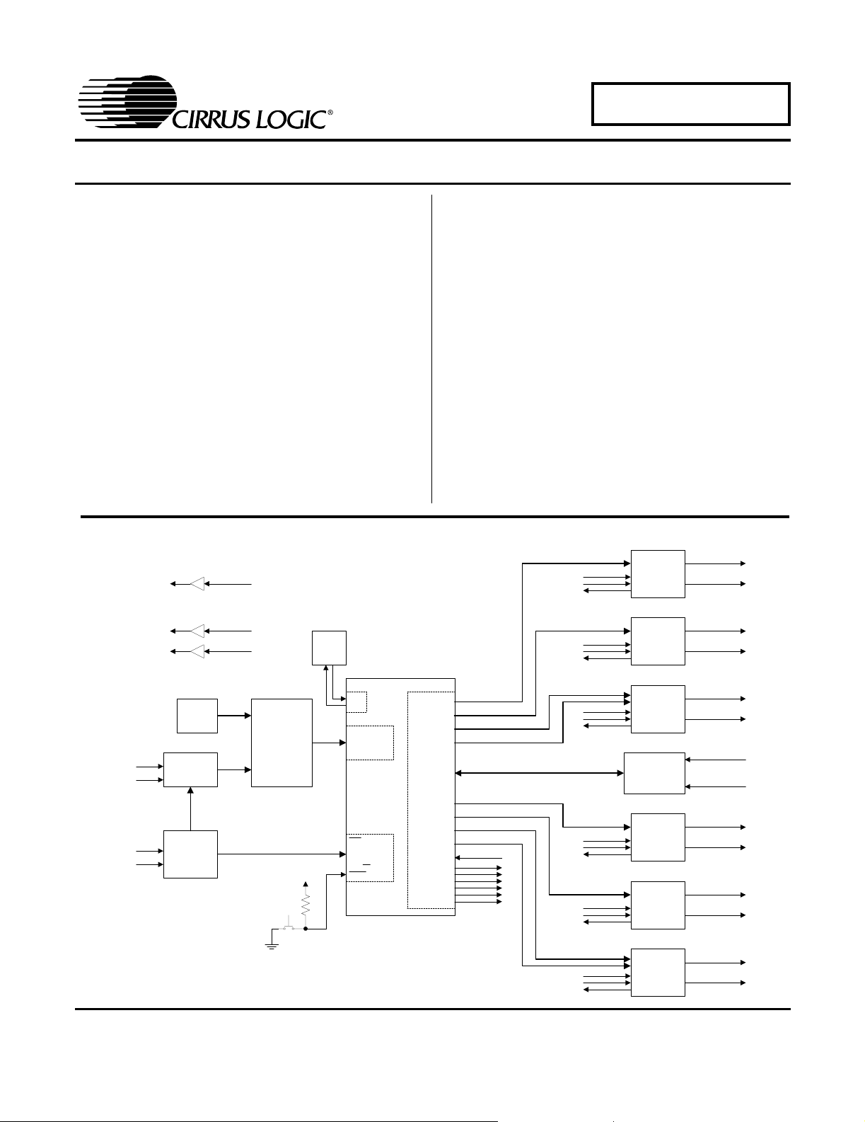
1. SYSTEM OVERVIEW
The CDB44800 demonstration board is an excellent means for evaluating the CS44800 eightchannel Class-D PWM modulator. It incorporates a digital audio interface, four full-bridge and 4
half-bridge configurations, and power supply rejection (PSR) circuitry, all on a two-layer board.
The CDB44800 schematic set is shown in Figures 4 through 12 and the board layout is shown
in Figures 13 through 15.
1.1 CS44800 PWM Modulator
A complete description of the CS44800 is included in the CS44800 product data sheet.
The CS44800 converts linear PCM data to pulse width modulated (PWM) output. It uses an
SRC to minimize jitter effects, resulting in high-quality sound output.
All supply voltages (VDX, VLS, VLC, and VDP) can be set using J30, J31, J32, and J28. A
push button is provided for immediate muting of the PWMOUTxxx outputs. PCM data and
clocks are input from either the CS8416 or J24 (PCM Input). J25 provides the SYS_CLK and
J21 provides the PS_SYNC output clocks for system development.
1.2 CS4461 PSR Feedback ADC
A complete description of the CS4461 is included in the CS4461 product data sheet.
The CS4461 is connected to the CS44800 to provide power supply rejection (PSR) for the
VP supply voltage connected to J17. Resistors R41 and R42 should be scaled for the supply
voltage used. See the CS4461 data sheet for equations to determine the resistor values.
The board comes initially populated with resistor values set for VP = 40 V.
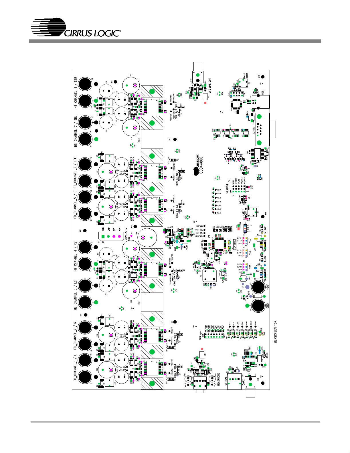
1.3 TDA8939 Power Stage
A complete description of the Philips TDA8939 is included in the TDA8939 product data
sheet.
The TDA8939 is a high-voltage PWM amplifier power stage. It integrates two half-bridge drivers and fault protection. With VP set to 40 V and R
to 65 W when set as a full-bridged output. With VP set to 40 V and R
can produce up to 35 W when set as a half-bridged output.
The supply voltage is set through J17 (VP) and should be between 20 V and 50 V. LEDs
D1 - D6 (DIAG) indicate a fault condition with the corresponding power stage. These signals
are OR’ed and input to GPIO0 pin on the CS44800. Speaker outputs are available from J1 J16. Care should be taken to not connect the full bridge black speaker connectors to ground
as these outputs are driven. The half bridge black speaker connectors can be connected directly to ground as these outputs are tied to ground on the board.
= 8 Ω, the TDA8939 can produce up
load
= 4 Ω, the TDA8939
load
1.4 CS8416 Digital Audio Receiver
The operation of the CS8416 receiver and a discussion of the digital audio interface are included in the CS8416 data sheet.
DS632DB2 3
Page 4

CDB44800
The CS8416 converts the input S/PDIF data stream into PCM data for the CS44800. The
CS8416 operates in master mode and can output either 128*Fs or 256*Fs from its RMCK pin.
Digital Interface format selection of I²S (24-bit), Left Justified (24-bit), or Right Justified (16 or
24-bit) can be made.
D20 (RERR) indicates a receiver error, such as loss of lock.
S/PDIF input is through OPT1 or J33.
1.5 Line and Headphone Outputs
An example of line level and headphone driver outputs are provided on the board. J18/J19
and J20 must be in place to connect the PWM outputs to drive the headphone and line outputs.
1.6 Control Port Interface and GUI
The CS44800 is controlled through the provided control port interface. Connections to the
control port can be made through J37 (RS-232 Serial) or J29 (External Control Header). A
Windows based GUI provides control over all the individual registers of the CS44800 and the
CS8416. To use the onboard control logic, J29 should be jumpered to “PC”. To use external
control logic J29 should have all jumpers removed and external signal and ground can be input through the pins labeled “EXT”. All external control signal levels should be referenced to
the VLC voltage setting of the board.
1.7 Power
Power must be supplied to the evaluation board through the +5.0 V binding post (J41). Onboard regulators supply +3.3 V and +2.5 V to the rest of the board. All voltage inputs must be
referenced to the single black banana-type ground connector (J40).
WARNING:Please refer to the CS44800 datasheet for allowable voltage levels.
1.8 Grounding and Power Supply Decoupling
The CS44800 requires careful attention to power supply and grounding arrangements to optimize performance. The block diagram on page 1 provides an overview of the connections
to the CS44800, Figure 13 shows the component placement, Figure 14 shows the top layout,
and Figure 15 shows the bottom layout. The 0.1µF ceramic decoupling capacitors are located as close to the power pins of the CS44800 as possible and on the same side of the board
as the CS44800. Extensive use of ground plane fill in the evaluation board yields large reductions in radiated noise.
1.9 Critical Component Selection
The output filter of the half-bridge and full-bridge outputs have components that must be chosen carefully.
The output snubbing resistors, R17-R40, used to shape the switching PWM output edges,
should be 5.6 Ω, ¼ W (VP = 30 V), ½ W (VP = 40 V), or 1 W (VP = 50 V) resistors. This board
is populated with DALE CRCW20105R62F parts.
4 DS632DB2
Page 5

CDB44800
The output snubbing capacitors, C43-C56, used to shape the switching PWM output edges,
should be 560 pF, C0G (NPO), with a voltage rating above the VP voltage. This board is populated with KEMET C0805C561K5GAC05R62F parts.
The output low-pass filter inductors, L1-L12, used to filter high frequency content from the
speakers, should be chosen so that their saturation current rating is above that of the maximum output current. This board is populated with TRANSTEK MAGNETICS TMP50627CT
and TMP50626CT parts.
The output low-pass filter capacitors, C13-C16, C18, C19, C21-C24, C26, and C27, used to
filter high frequency content from the speakers, should be chosen to have a dielectric of metallized film, with a voltage rating above the VP voltage. This board is populated with PANASONIC ECQV1H474JL and ECQV1H105JL parts.
The half-bridge channels output high-pass filter capacitors, C17, C20, C25, and C28, used
to filter DC frequency content from the speakers, should have a ripple current rating above
the maximum peak output current and have a voltage rating above the maximum peak output
voltage. This board is populated with PANASONIC ECA1HM102 parts. The capacitance value determines the cutoff frequency of the high-pass filter. The cutoff frequency (-3 dB point)
on the board has been set for 26 Hz when used with a 6 Ω load.
The VP power supply bulk decoupling capacitors, C29-C32 and C57-C60 should be chosen
to have a voltage rating above the VP voltage. The lower the capacitor’s ESR rating at the
working frequency, the better the noise attenuation. Low ESR decoupling capacitors will offer lower output speaker noise than high ESR capacitors. This board is populated with
NICHICON UPW1J102MHH parts.
The Zoble filter network resistors, R1-R12, used to impedance match the speaker, should be
chosen to have a power handling according to the following equation: P = C * V² * f. For this
board, C = 0.22 µF, f = 20 kHz, and V = the RMS full-scale output voltage. This board is populated with 1 W DALE CRCW251222R1F parts.
DS632DB2 5
Page 6
CDB44800
Reference
CONNECTOR
+5V J36 Input +5.0 V Power Supply
GND J35 Input Ground Reference
VDX J30 Input +2.5 V, +3.3 V, or +5.0 V Power Supply for VDX
VLS J31 Input +2.5 V, +3.3 V, or +5.0 V Power Supply for VLS
VLC J32 Input +2.5 V, +3.3 V, or +5.0 V Power Supply for VLC
VDP J28 Input +3.3 V or +5.0 V Power Supply for VDP
COAX IN J33 Input CS8416 digital audio input via coaxial cable
OPTICAL IN OPT1 Input CS8416 digital audio input via optical cable
PCM Input J24 Input Input for PCM Clocks and Data
HEADPHONE J23 Output Headphone Driver Output
LFE LINE OUT J22 Output Line Level Output for LFE Channel
SERIAL J37 Input Serial Control Port Interface
VP J17 Input +20 V to +50 V Power Supply for the TDA8939 Output Power
FB_CHANNEL_1/L J1
FB_CHANNEL_2/R J3
HB_CHANNEL_3/LS J5
HB_CHANNEL_4/RS J7
FB_CHANNEL_5/C J9
FB_CHANNEL_6/LFE J11
HB_CHANNEL_7/SBL J13
HB_CHANNEL_8/SBR J15
Designator
J2
J4
J6
J8
J10
J12
J14
J16
INPUT /
OUTPUT SIGNAL PRESENT
Stages
Output
Output
Output
Output
Output
Output
Output
Output
Output
Output
Output
Output
Output
Output
Output
Output
Positive and Negative Full Bridge Outputs for Channel 1 / Left
Positive and Negative Full Bridge Outputs for Channel 2 / Right
Positive Half Bridge Output and Ground Reference for Channel
3 / Left Surround
Positive Half Bridge Output and Ground Reference for Channel
4 / Right Surround
Positive and Negative Full Bridge Outputs for Chann el 5 / Center
Positive and Negative Full Bridge Outputs for Channel 6 / Low
Frequency Effects (Subwoofer)
Positive Half Bridge Output and Ground Reference for Channel
7 / Surround Back Left
Positive Half Bridge Output and Ground Reference for Channel
8 / Surround Back Right
Table 1. System Connections
6 DS632DB2
Page 7
CDB44800
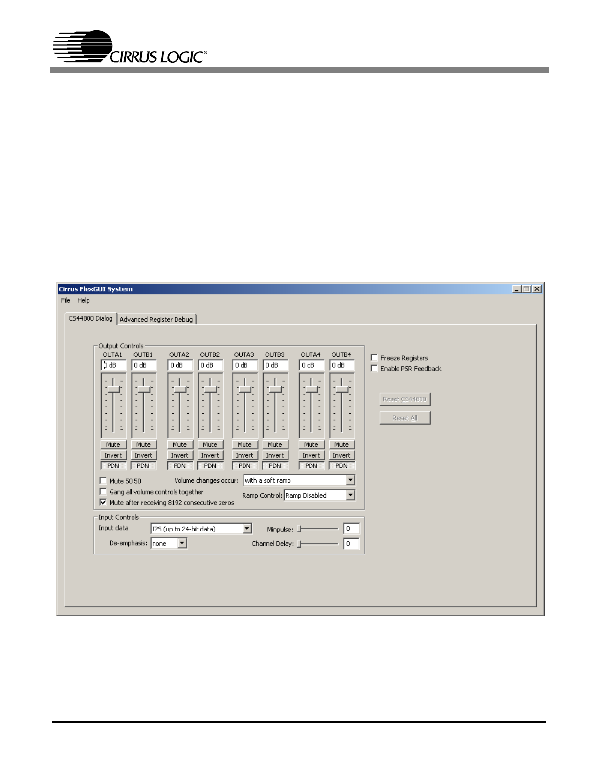
2. GUI CONTROL
The CDB44800 is shipped with a Microsoft Windows® based GUI, which allows control over the
CS8416 and CS44800 registers. Interface to the CDB44800 control port is provided using an RS232 serial cable. Once the appropriate cable is connected between the CDB44800 and the host
PC, load the FlexLoader.exe from the CDB44800 directory. Once loaded, all registers are set to
their default reset state. The GUI File menu provides the ability to save and restore (load) script
files containing all of the register settings. Sample script files are provided for basic functionality.
2.1 CS44800 Dialog Tab
The CS44800 Dialog tab provides high level control over the CS44800’s registers. Controls
are provided to change volume, mute, power down, ramp, SAI input format, minimum pulse
width, and channel delay.
Figure 1. CS44800 Dialog Tab
DS632DB2 7
Page 8
CDB44800
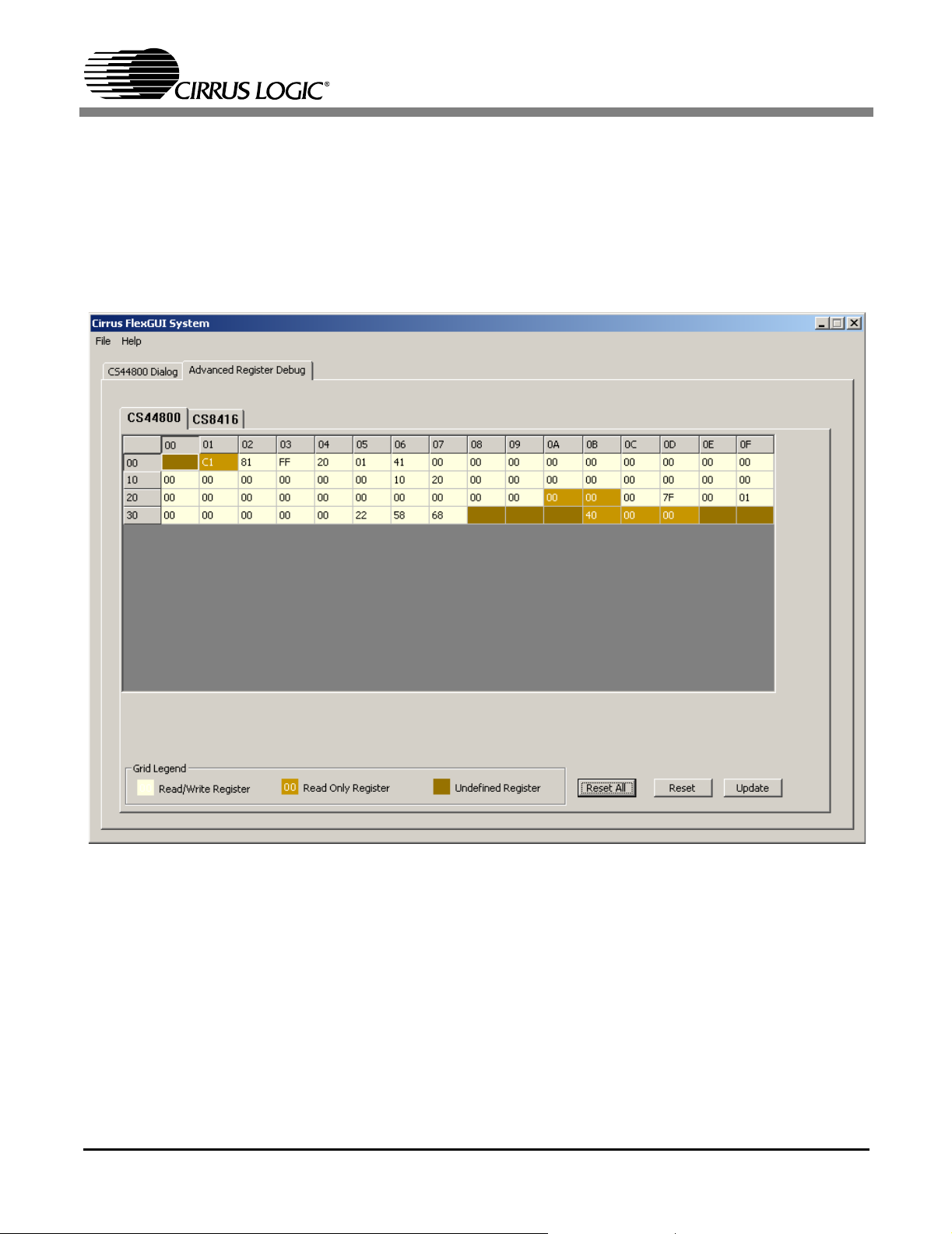
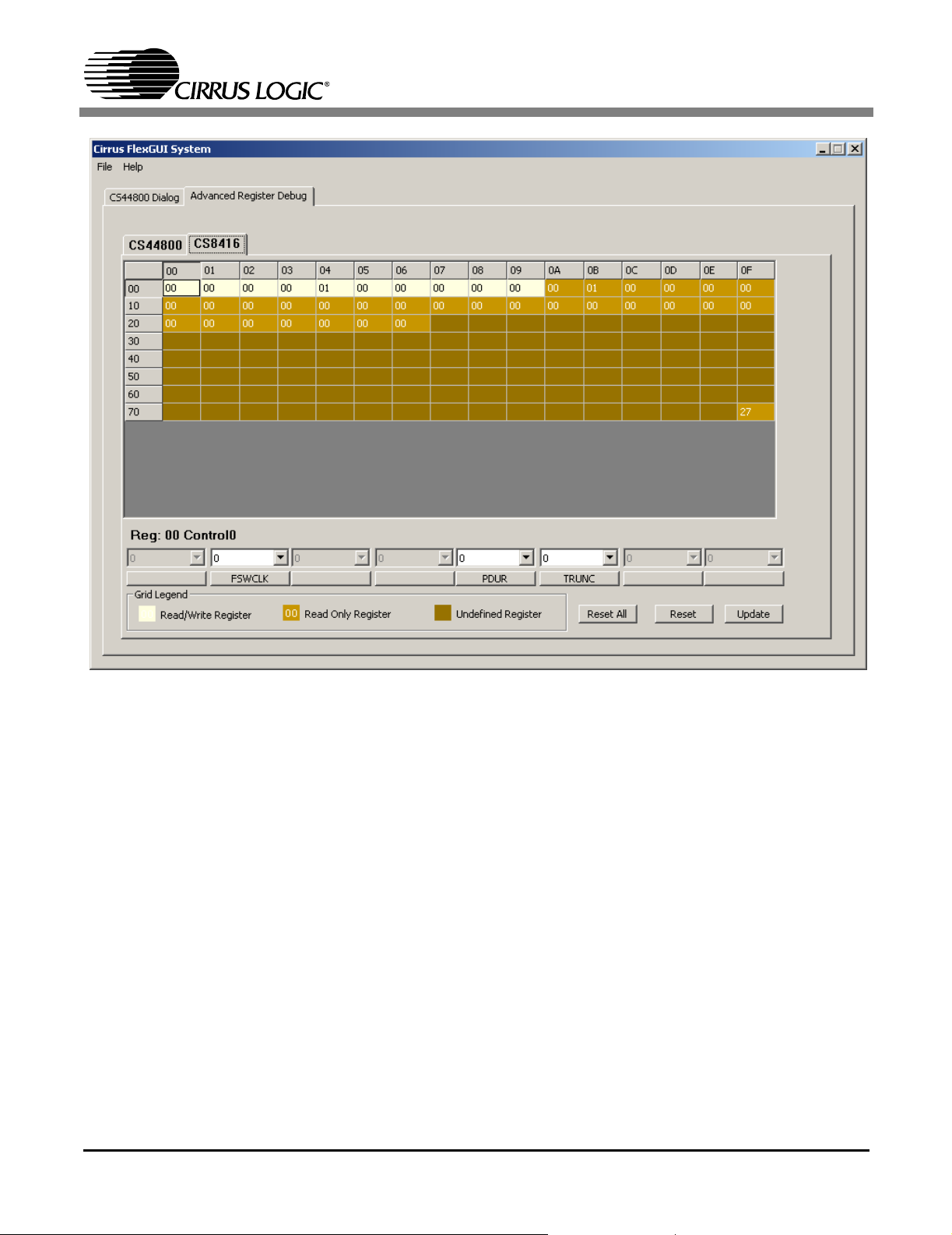
2.2 Advanced Register Debug Tab
The Advanced Register Debug tab provides low level control over the CS44800 and CS8416
individual register settings. Each device is displayed on a separate tab. Register values can
be modified bitwise or bytewise. For bitwise, click the appropriate push button for the desired
bit. For bytewise, the desired hex value can be typed directly in the register address box in
the register map.
Figure 2. Advanced Register Debug Tab - CS44800
8 DS632DB2
Page 9
CDB44800
Figure 3. Advanced Register Debug Tab - CS8416
DS632DB2 9
Page 10

3. SCHEMATICS
CDB44800
Figure 4. Power
10 DS632DB2
Page 11

CDB44800
Figure 5. CS8416
DS632DB2 11
Page 12

CDB44800
Figure 6. CS44800
12 DS632DB2
Page 13

CDB44800
Figure 7. CS4461 PSR Feedback
DS632DB2 13
Page 14

CDB44800
Figure 8. Half Bridge Channels
14 DS632DB2
Page 15

CDB44800
Figure 9. Full Bridge Channels 1
DS632DB2 15
Page 16

CDB44800
Figure 10. Full Bridge Channels 2
16 DS632DB2
Page 17

CDB44800
Figure 11. Analog Outputs
DS632DB2 17
Page 18

CDB44800
Figure 12. Control Port
18 DS632DB2
Page 19
4. LAYOUT
CDB44800
Figure 13. Silk Screen
DS632DB2 19
Page 20

CDB44800
Figure 14. Topside Layer
20 DS632DB2
Page 21

CDB44800
Figure 15. Bottomside Layer
DS632DB2 21
Page 22
5. REVISION HISTORY
Release Date Changes
DB1 June 2004 1st Release
DB2 October 2004 Updated sections to reflect board revision B changes:
-Updated “CS44800 PWM Modulator” on page 3
-Updated “CS4461 PSR Feedback ADC” on page 3
-Updated “TDA8939 Power Stage” on page 3
-Updated “CS8416 Digital Audio Receiver” on page 3
-Updated “Line and Headphone Outputs” on page 4
-Updated “Control Port Interface and GUI” on page 4
-Added “Critical Component Selection” on page 4
-Updated Table 1 on page 6
-Updated “CS44800 Dialog Tab” on page 7
-Updated Figure 1 on page 7
-Updated Figure 2 on page 8
-Updated Figure 4 on page 10
-Updated Figure 5 on page 11
-Updated Figure 6 on page 12
-Updated Figure 7 on page 13
-Updated Figure 8 on page 14
-Updated Figure 9 on page 15
-Updated Figure 10 on page 16
-Updated Figure 11 on page 17
-Updated Figure 12 on page 18
-Updated Figure 13 on page 19
-Updated Figure 14 on page 20
-Updated Figure 15 on page 21
CDB44800
Table 2. Revision History
22 DS632DB2
Page 23

CDB44800
Contacting Cirrus Logic Support
For all product questions and inquiries contact a Cirrus Logic Sales Representative.
To find one nearest you go to <http://www.cirrus.com/corporate/contacts/sales.cfm>
IMPORTANT NOTICE
Cirrus Logic, Inc. and it s s ubs i di ari es (“ Ci rr us ”) beli e ve t hat th e i nf or mat i on c ont ai ne d i n th i s docu ment is ac cur ate an d rel i able. However, the information is subject
to change without not ice and i s provid ed “AS IS” wit hout war ranty of any kind (ex press or i mplied) . Custome rs are advi sed to obt ain the late st version of relevant
information to verify, before placing orders, that information being relied on is current and complete. All products are sold subject to the terms and conditions of sale
supplied at the time of order acknowledgment, including those pertaining to warranty, patent infringement, and limitation of liability. No responsibility is assumed by
Cirrus for the use of this information, including use of this information as the basis for manufacture or sale of any items, or for infringement of patents or other rights
of third parties. This document is the property of Cirrus and by furnishing this information, Cirrus grants no license, express or implied under any patents, mask work
rights, copyrights, trademarks, trade secrets or othe r intellectual proper ty rights. Cirrus owns the copyrights of the information contained herein and gives consent for
copies to be made of the information only for use within your organization with respect to Cirrus integrated circuits or other parts of Cirrus. Thi s consent does not
extend to other copying such as copying for general distribution, advertising or promotional purposes, or for creating any work for resale.
CERTAIN APPLICATIONS USING SEMI CONDUCTOR P RODUCT S MAY I NVOL VE PO TENT I AL RI SKS OF DEAT H, PE RS ONAL IN JU RY, OR S EV ERE PRO PERTY OR ENVIRONMENTAL DAMAGE (“CRITICAL APPLICATIONS”). CIRRUS PRODUCTS ARE NOT DESIGNED, AUTHORIZED OR WARRANTED FOR USE
IN AIRCRAFT SYSTEMS, MILITARY APPLICATIONS, PRODUCTS SURGICALLY IMPLANTED INTO THE BODY, LIFE SUPPORT PRODUCTS OR OTHER CRITICAL APPLICATIONS (INCLUDING MEDICAL DEVICES, AIRCRAFT SYSTEMS OR COMPONENTS AND PERSONAL OR AUTOMOTIVE SAFETY OR SECURITY DEVICES). INCLUSION OF CIRRUS PRODUCTS IN SUCH APPLICATIONS IS UNDERSTOOD TO BE FULLY AT THE CUSTOMER’S RISK AND CIRRUS
DISCLAIMS AND MAKES NO WARRANTY, EXPRESS, STATUTORY OR IMPLIED, INCLUDING THE IMPLIED WARRANTIES OF MERCHANTABILITY AND FITNESS FOR PARTICULAR PURPOSE, WITH REGARD TO ANY CIRRUS PRODUCT THAT IS USED IN SUCH A MANNER. IF THE CUSTOMER OR CUSTOMER’S CUSTOMER USES OR PERMITS THE USE OF CIRRUS PRODUCTS IN CRITICAL APPLI CATIONS, CUSTO MER AGREES, BY SUCH US E, TO FULLY
INDEMNIFY CIRRUS, ITS OFFICERS, DIRECTORS, EMPLOYEES, DISTRIBUTORS AND OTHER AGENTS FROM ANY AND ALL LIABILITY, INCLUDING ATTORNEYS’ FEES AND COSTS, THAT MAY RESULT FROM OR ARISE IN CONNECTION WITH THESE USES.
Cirrus Logic, Cirrus, and the Cirrus Log ic lo go d esi gn s ar e trademarks of Cirrus Logic, Inc. All other brand an d product names in this document may be tradem arks
or service marks of their respective owners.
Microsoft Windows is a registered trademark of Microsoft Corporation.
DS632DB2 23
Page 24

CDB44800
24 DS632DB2
 Loading...