

Page 1
Evaluation Board for CS4384
CDB4384
Features
Demonstrates recommended layout and
grounding arrangements.
CS8416 receives S/PDIF, & EIAJ-340
compatible digital audio.
Headers for external audio input for either
PCM or DSD.
Requires only a digital signal source and
power supplies for a complete Digital-to-analog
converter system.
Inputs for PCM
Clocks and Data
Description
The CDB4384 evaluation board is an excellent means
for quickly evaluating the CS4384 24-bit, 48-pin, 8channel, single-ended D/A converter. Evaluation requires an analog signal analyzer, a digital signal source,
a PC for controlling the CS4384 (only required for control port mode), and a power supply. Analog line-level
outputs are provided via RCA phono jacks.
The CS8416 digital audio receiver IC provides the system timing necessary to operate the digital-to-analog
converter and will accept S/PDIF and EIAJ-340-compatible audio data. The evaluation board may also be
configured to accept external timing and data signals for
operation in a user application during system
development.
ORDERING INFORMATION
CDB4384 Evaluation Board
Hardware or
Software Board
Control
CS8416
Digital Audio
Interface
Inputs for DSD
Clocks and Data
http://www.cirrus.com
CS4384
Copyright © Cirrus Logic, Inc. 2005
(All Rights Reserved)
Analog Outputs
and Filtering
JULY '05
DS620DB1
Page 2

TABLE OF CONTENTS
1. CS4384 DIGITAL TO ANALOG CONVERTER . . . . . . . . . . . . . . . . . . . . . . . . . . . . . . . . . . . . 3
2. CS8416 DIGITAL AUDIO RECEIVER . . . . . . . . . . . . . . . . . . . . . . . . . . . . . . . . . . . . . . . . . . . 3
3. INPUT FOR CLOCKS AND DATA . . . . . . . . . . . . . . . . . . . . . . . . . . . . . . . . . . . . . . . . . . . . . . 3
4. INPUT FOR CONTROL DATA . . . . . . . . . . . . . . . . . . . . . . . . . . . . . . . . . . . . . . . . . . . . . . . . . 3
5. POWER SUPPLY CIRCUITRY . . . . . . . . . . . . . . . . . . . . . . . . . . . . . . . . . . . . . . . . . . . . . . . . . 4
6. GROUNDING AND POWER SUPPLY DECOUPLING . . . . . . . . . . . . . . . . . . . . . . . . . . . . . . 4
7. ANALOG OUTPUT FILTERING . . . . . . . . . . . . . . . . . . . . . . . . . . . . . . . . . . . . . . . . . . . . . . . . 4
8. ERRATA . . . . . . . . . . . . . . . . . . . . . . . . . . . . . . . . . . . . . . . . . . . . . . . . . . . . . . . . . . . . . . . . . . 5
9. SCHEMATICS . . . . . . . . . . . . . . . . . . . . . . . . . . . . . . . . . . . . . . . . . . . . . . . . . . . . . . . . . . . . 6
LIST OF FIGURES
Figure 1. System Block Diagram and Signal Flow. . . . . . . . . . . . . . . . . . . . . . . . . . . . . . . . . . . 6
CDB4384
Figure 2. CS4384 . . . . . . . . . . . . . . . . . . . . . . . . . . . . . . . . . . . . . . . . . . . . . . . . . . . . . . . . . . . . . . 7
Figure 3. Analog Output Pairs 1 & 2 . . . . . . . . . . . . . . . . . . . . . . . . . . . . . . . . . . . . . . . . . . . . . . 8
Figure 4. Analog Output Pairs 3 & 4 . . . . . . . . . . . . . . . . . . . . . . . . . . . . . . . . . . . . . . . . . . . . . . 9
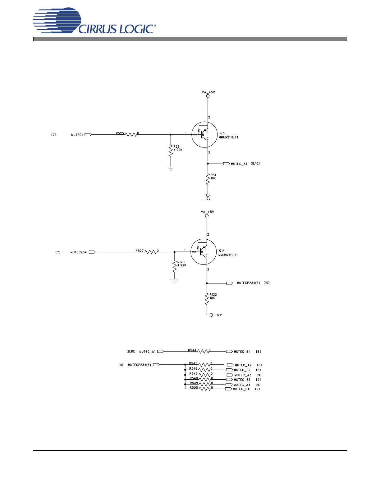
Figure 5. Mute Circuits . . . . . . . . . . . . . . . . . . . . . . . . . . . . . . . . . . . . . . . . . . . . . . . . . . . . . . . . 10
Figure 6. CS8416 S/PDIF Input. . . . . . . . . . . . . . . . . . . . . . . . . . . . . . . . . . . . . . . . . . . . . . . . . .11
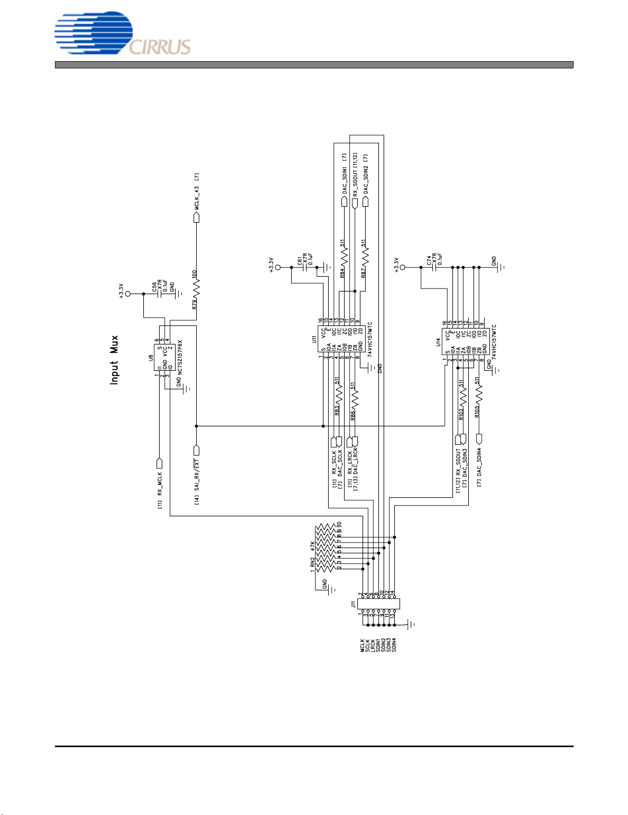
Figure 7. PCM input Header and Muxing . . . . . . . . . . . . . . . . . . . . . . . . . . . . . . . . . . . . . . . . . 12
Figure 8. DSD input Header . . . . . . . . . . . . . . . . . . . . . . . . . . . . . . . . . . . . . . . . . . . . . . . . . . . . 13
Figure 9. Control Input . . . . . . . . . . . . . . . . . . . . . . . . . . . . . . . . . . . . . . . . . . . . . . . . . . . . . . . . 14
Figure 10. Power inputs . . . . . . . . . . . . . . . . . . . . . . . . . . . . . . . . . . . . . . . . . . . . . . . . . . . . . . . 15
Figure 11. Silkscreen Top. . . . . . . . . . . . . . . . . . . . . . . . . . . . . . . . . . . . . . . . . . . . . . . . . . . . . . 16
Figure 12. Top Side . . . . . . . . . . . . . . . . . . . . . . . . . . . . . . . . . . . . . . . . . . . . . . . . . . . . . . . . . . . 17
Figure 13. Bottom Side . . . . . . . . . . . . . . . . . . . . . . . . . . . . . . . . . . . . . . . . . . . . . . . . . . . . . . . . 18
2 DS620DB1
Page 3

CDB4384
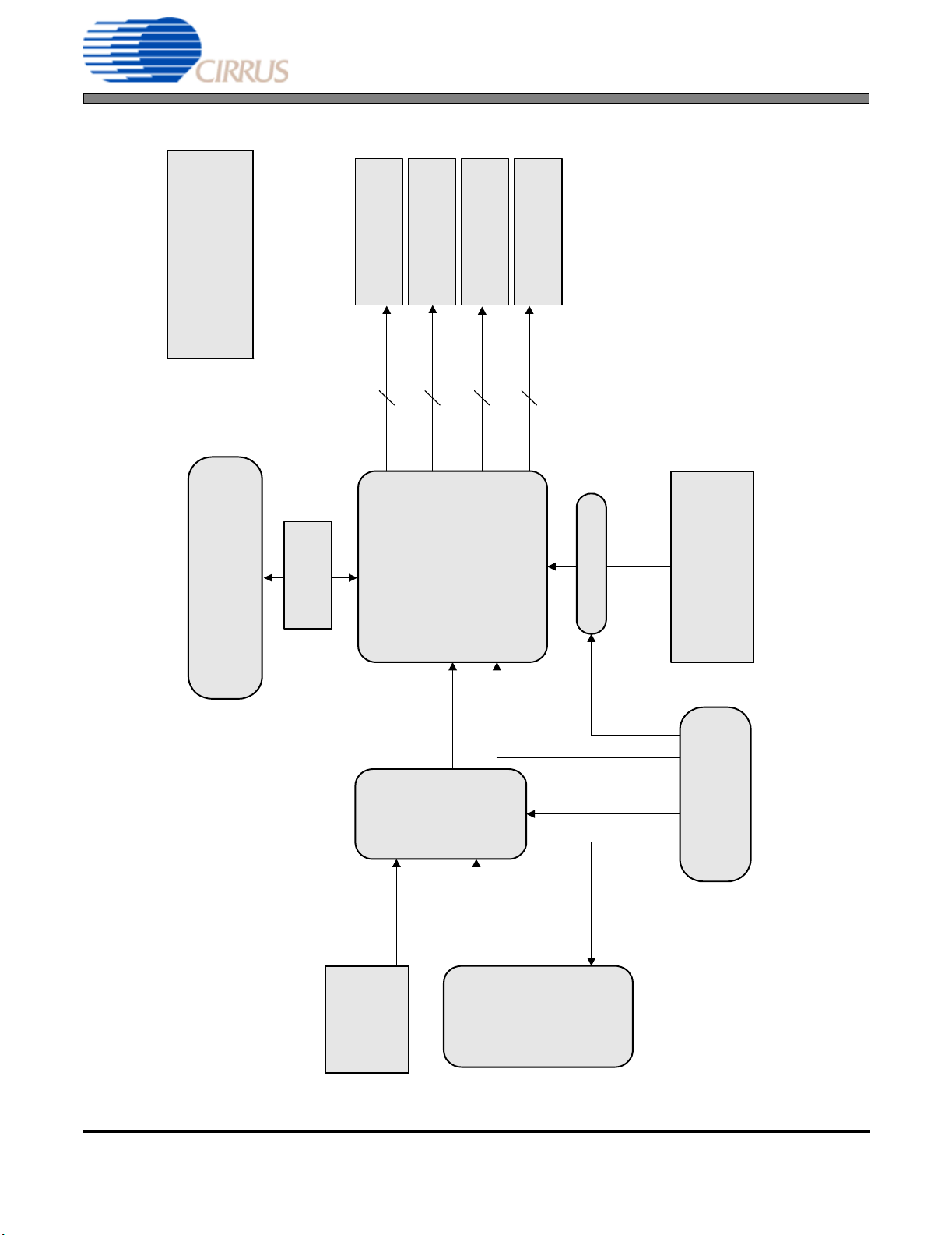
CDB4384 SYSTEM OVERVIEW
The CDB4384 evaluation board is an excellent means of quickly evaluating the CS4384. The CS8416 digital audio
interface receiver provides an easy interface to digital audio signal sources including the majority of digital audio
test equipment. The evaluation board also allows the user to supply external PCM or DSD clocks and data through
PCB headers for system development.
The CDB4384 uses the CDB4385 as a base PCB board. For this reason, there may be additional circuitry on board
which is not populated as it has no function for this device.
The CDB4384 schematic has been partitioned into 9 schematics shown in Figures 2 through 10. Each partitioned
schematic is represented in the system diagram shown in Figure 1. Notice that the system diagram also includes
the interconnections between the partitioned schematics.
1. CS4384 DIGITAL TO ANALOG CONVERTER
A description of the CS4384 is included in the CS4384 datasheet.
2. CS8416 DIGITAL AUDIO RECEIVER
The system receives and decodes the standard S/PDIF data format using a CS8416 digital audio receiver (Figure
6). The outputs of the CS8416 include a serial bit clock, serial data, left-right clock, and a 128/256 Fs master clock.
The CS8416 data format is fixed to I
is included in the CS8416 datasheet.
²S. The operation of the CS8416 and a discussion of the digital audio interface
The evaluation board has been designed such that the input can be either optical or coaxial, see Figure 6. However,
both inputs cannot be driven simultaneously.
Switch position 7 of S1 sets the output MCLK-to-LRCK ratio of the CS8416. This switch should be set to 256 (closed)
for inputs Fs ≤ 96 kHz and 128 (open) for Fs ≥ 64 kHz. The CS8416 must be manually reset using ‘HW RST’ (S2)
or through the software when this switch is changed.
3. INPUT FOR CLOCKS AND DATA
The evaluation board has been designed to allow interfacing to external systems via headers J11 and J7. Header
J11 allows the evaluation board to accept externally generated PCM clocks and data. The schematic for the
clock/data input is shown in Figure 7. Switch position 6 of S1 selects the source as either CS8416 (open) or header
J11 (closed).
Header J7 allows the evaluation board to accept externally generated DSD data and clocks. The schematic for the
clock/data input is shown in Figure 8. A synchronous MCLK must still be provided via Header J11. Switch position
8 of S1 selects either PCM (open) or DSD (closed).
Please see the CS4384 datasheet for more information.
4. INPUT FOR CONTROL DATA
The evaluation board can be run in either a stand-alone mode or with a PC. Stand-alone mode uses the CS4384 in
hardware mode and the mode pins are configured using switch positions 1 through 5 of S1. PC mode uses software
to setup the CS4384 through I
(RS232 or USB) is attached and the CDB4384 software is running. The latest control software may be downloaded
from: www.cirrus.com/msasoftware.
²C using the PC’s serial port. PC mode is automatically selected when the serial port
Header J15 offers the option for external input of RST and SPI
factory to use the on-board microcontroller in conjunction with the supplied software. To use an external control
DS620DB1 3
™/I²C clocks and data. The board is setup from the
Page 4
CDB4384
source, remove the shunts on J15 and place a ribbon cable so the signal lines are on the center row and the grounds
are on the right side. R116 and R119 should be populated with 2 kΩ resistors when using an external I
which does not already provide pull-ups.
²C source
5. POWER SUPPLY CIRCUITRY
Power is supplied to the evaluation board by four binding posts (GND, +5V, +12V, and -12V), see Figure 10. The
‘+5V’ terminal supplies VA and the rest of the +5 V circuitry on the board. The +3.3 V circuitry is powered from a
regulator. The +2.5 V required for VD is also provided from an on-board regulator. The +5 V supply should be set
within the recommended values for VA stated in the CS4384 datasheet.
WARNING: Refer to the CS4384 datasheet for maximum allowable voltage levels. Operation outside of this range
can cause permanent damage to the device.
6. GROUNDING AND POWER SUPPLY DECOUPLING
As with any high-performance converter, the CS4384 requires careful attention to power supply and grounding arrangements to optimize performance. Figure 2 details the connections to the CS4384 and Figures 11, 12, and 13
show the component placement and top and bottom layout. The decoupling capacitors are located as close to the
CS4384 as possible. Extensive use of ground plane fill in the evaluation board yields large reductions in radiated
noise.
7. ANALOG OUTPUT FILTERING
The analog output on the CDB4384 has been designed according to the CS4384 datasheet. This output circuit includes a passive 1-pole, 150 kHz filter with an AC coupled output.
CONNECTOR INPUT/OUTPUT SIGNAL PRESENT
+5V Input + 5 V power
GND Input Ground connection from power supply
+12V Input Unused
-12V Input Negative supply for the mute circuitry (-5 V to -12 V)
S/PDIF IN - J9 Input Digital audio interface input via coax
S/PDIF IN - OPT1 Input Digital audio interface input via optical
PCM INPUT - J11 Input Input for master, serial, left/right clocks and serial data
DSD INPUT - J7 Input Input for DSD serial clock and DSD data
OUTA1-B4 Output RCA line level analog outputs
Table 1. System Connections
4 DS620DB1
Page 5
JUMPER /
SWITCH PURPOSE POSITION FUNCTION SELECTED
J15
J16 JTAG micro programming - Reserved for factory use only
S2
S1
*Default Factory Settings.
Selects source of control
data
Resets CS8416 and
CS4384
CS4384 mode settings M0-
M4
Sets clock source 6
Sets MCLK ratio of CS8416 7
Selects PCM or DSD mode 8 For PCM input set to *Open, for DSD set to Closed
*shunts on Left
shunts removed
1-5
Table 2. CDB4384 Jumper Settings
*Control from PC and on-board microcontroller
External control input using center and right columns
The CS8416 must be reset if switch S1 is changed
*open = RX(CS8416), closed = EXT
Selects 128x (open) or 256x
Default: M0, M4 open (HI)
M1, M2, M3 closed (LO)
Sets clock source for CS4384
(*closed) MCLK/LRCK
ratio output for CS8416
CDB4384
(J11)
8. ERRATA
CDB4384 rev C.
-None at this time.
DS620DB1 5
Page 6
CDB4384
Outputs
Power
Figure 10 on page 15
Single-Ended Analog
A1, B1
A2, B2
Figure 3 on page 8
A3, B3
Figure 3 on page 8
A4, B4
Figure 4 on page 9
Figure 4 on page 9
2
C/SPI Header
2
I
Figure 9 on page 14
Serial Control Port
2
2
2
Figure 2 on page 7
CS4384
PCM Clocks/Data
DSD clk_enable
Data
DSD Clocks/
DSD HEADER
Figure 8 on page 13
DSD input enable
(for stand-alone mode)
M0 - M4 switches
PCM source select
Switches
PCM mux
Figure 7 on
page 12
CS8416 clock setting
Hardware Control
Figure 9 on page 14
PCM Clocks/Data
Input
S/PDIF
CS8416
Figure 6 on
page 11
PCM HEADER
PCM Clocks/Data
Figure 7 on
page 12
Figure 1. System Block Diagram and Signal Flow
9. SCHEMATICS
6 DS620DB1
Page 7

CDB4384
Figure 2. CS4384
DS620DB1 7
Page 8

CDB4384
Figure 3. Analog Output Pairs 1 & 2
8 DS620DB1
Page 9

CDB4384
Figure 4. Analog Output Pairs 3 & 4
DS620DB1 9
Page 10
CDB4384
Figure 5. Mute Circuits
10 DS620DB1
Page 11

CDB4384
Figure 6. CS8416 S/PDIF Input
DS620DB1 11
Page 12
CDB4384
Figure 7. PCM input Header and Muxing
12 DS620DB1
Page 13

CDB4384
Figure 8. DSD Input Header
DS620DB1 13
Page 14

CDB4384
Figure 9. Control Input
14 DS620DB1
Page 15

CDB4384
Figure 10. Power Inputs
DS620DB1 15
Page 16

CDB4384
Figure 11. Silkscreen Top
16 DS620DB1
Page 17

CDB4384
Figure 12. Top Side
DS620DB1 17
Page 18

CDB4384
Figure 13. Bottom Side
18 DS620DB1
Page 19

CDB4384
REVISION HISTORY
Release Date Changes
DB1 JULY 2005 Initial Release
Contacting Cirrus Logic Support
For all product questions and inquiries contact a Cirrus Logic Sales Representative.
To find the one nearest to you go to www.cirrus.com
IMPORTANT NOTICE
Cirrus Logic, Inc. and its subsidiaries ("Cirrus") believe that the information contained in this document is accurate and reliable. However, the information is subject to change without notice and is provided "AS IS" without warranty of any kind (express or implied). Customers are advised to obtain the latest version of
relevant information to verify, before placing orders, that information being relied on is current and complete. All products are sold subject to the terms and conditions of sale supplied at the time of order acknowledgment, including those pertaining to warranty, indemnification, and limitation of liability. No responsibility
is assumed by Cirrus for the use of this information, including use of this information as the basis for manufacture or sale of any items, or for infringement of
patents or other rights of third parties. This document is the property of Cirrus and by furnishing this information, Cirrus grants no license, express or implied
under any patents, mask work rights, copyrights, trademarks, trade secrets or other intellectual property rights. Cirrus owns the copyrights associated with the
information contained herein and gives consent for copies to be made of the information only for use within your organization with respect to Cirrus integrated
circuits or other products of Cirrus. This consent does not extend to other copying such as copying for general distribution, advertising or promotional purposes,
or for creating any work for resale.
CERTAIN APPLICATIONS USING SEMICONDUCTOR PRODUCTS MAY INVOLVE POTENTIAL RISKS OF DEATH, PERSONAL INJURY, OR SEVERE
PROPERTY OR ENVIRONMENTAL DAMAGE ("CRITICAL APPLICATIONS"). CIRRUS PRODUCTS ARE NOT DESIGNED, AUTHORIZED OR WARRANTED FOR USE IN AIRCRAFT SYSTEMS, MILITARY APPLICATIONS, PRODUCTS SURGICALLY IMPLANTED INTO THE BODY, AUTOMOTIVE SAFETY OR
SECURITY DEVICES, LIFE SUPPORT PRODUCTS OR OTHER CRITICAL APPLICATIONS. INCLUSION OF CIRRUS PRODUCTS IN SUCH APPLICATIONS IS UNDERSTOOD TO BE FULLY AT THE CUSTOMER'S RISK AND CIRRUS DISCLAIMS AND MAKES NO WARRANTY, EXPRESS, STATUTORY
OR IMPLIED, INCLUDING THE IMPLIED WARRANTIES OF MERCHANTABILITY AND FITNESS FOR PARTICULAR PURPOSE, WITH REGARD TO ANY
CIRRUS PRODUCT THAT IS USED IN SUCH A MANNER. IF THE CUSTOMER OR CUSTOMER'S CUSTOMER USES OR PERMITS THE USE OF CIRRUS
PRODUCTS IN CRITICAL APPLICATIONS, CUSTOMER AGREES, BY SUCH USE, TO FULLY INDEMNIFY CIRRUS, ITS OFFICERS, DIRECTORS, EMPLOYEES, DISTRIBUTORS AND OTHER AGENTS FROM ANY AND ALL LIABILITY, INCLUDING ATTORNEYS' FEES AND COSTS, THAT MAY RESULT
FROM OR ARISE IN CONNECTION WITH THESE USES.
Cirrus Logic, Cirrus, and the Cirrus Logic logo designs are trademarks of Cirrus Logic, Inc. All other brand and product names in this document may be trademarks or service marks of their respective owners.
SPI is a trademark of Motorola, Inc.
DS620DB1 19
 Loading...