

Page 1
Evaluation Board for CS4365
CDB4365
Features
Demonstrates recommended layout and
grounding arrangements
CS8416 receives S/PDIF, & EIAJ-340
compatible digital audio
Headers for external audio input for either PCM
or DSD
Requires only a digital signal source and power
supplies for a complete Digital-to-analog
converter system
®
Description
The CDB4365 evaluation board is an excellent means
for quickly evaluating the CS4365 24-bit, 48-pin, 6channel D/A converter. Evaluation requires an analog
signal analyzer, a digital signal source, a PC for controlling the CS4365 (only required for control port mode),
and a power supply. Analog line-level outputs are provided via RCA phono jacks.
The CS8416 digital audio receiver IC provides the system timing necessary to operate the digital-to-analog
converter and will accept S/PDIF and EIAJ-340-compatible audio data. The evaluat ion board may also be
configured to accept external timing and data signals for
operation in a user application during system
development.
ORDERING INFORMATION
CDB4365 Evaluation Board
Inputs for PCM
Clocks and Data
CS8416
Digital Audio
Interface
Inputs for DSD
Clocks and Data
Hardware or
Software Board
Control
CS4365
Analog Outputs
and Filtering
http://www.cirrus.com
Copyright © Cirrus Logic, Inc. 2008
(All Rights Reserved)
MAY '08
DS670DB3
Page 2

TABLE OF CONTENTS
1. CS4365 DIGITAL-TO-ANALOG CONVERTER ..................................................................................... 4
2. CS8416 DIGITAL AUDIO RECEIVER .................................................................................................... 4
3. INPUT FOR CLOCKS AND DATA ......................................................................................................... 4
4. INPUT FOR CONTROL DATA ............................................................................................................... 4
5. POWER SUPPLY CIRCUITRY ............................................................................................................... 5
6. GROUNDING AND POWER SUPPLY DECOUPLING .......................................................................... 5
7. ANALOG OUTPUT FILTERING ........................... ................................................ .... ... ... ... ..................... 5
8. PERFORMANCE PLOTS ....................................................................................................................... 7
9. CDB4365 SCHEMATICS ..................................................................................................................... 17
10. REVISION HISTORY ......................................................................................................................... 30
LIST OF FIGURES
Figure 1.FFT (48 kHz, 0 dB) ............................................... ... ... ... .... ... ... ... .................................................. 7
Figure 2.FFT (48 kHz, -60 dB) ........................... .... ... ... ... .... ... ... ... .... ... ... ..................................................... 7
Figure 3.FFT (48 kHz, No Input) ................................................................................................................. 7
Figure 4.FFT (48 kHz Out-of-Band, No Input) ............................................................................................. 7
Figure 5.FFT (48 kHz, -60 dB Wideband) .............. ... ... ... .... ... ................................................... .... .............. 8
Figure 6.FFT (IMD 48 kHz) ......................................................................................................................... 8
Figure 7.48 kHz, THD+N vs. Input Freq . ... ... ... ... .... ... ... ... .... ... ... ................................................ .... .............. 8
Figure 8.48 kHz, THD+N vs. Level ................. ... .... ... ... ... .... ................................................ ... ... .................. 8
Figure 9.48 kHz, Fade-to-Noise Linearity ........................................... ... ... ... .... ... ... ... .... ... ... ... ... .... .............. 8
Figure 10.48 kHz, Frequency Response ......................... .... ... ................................................ ... .... ... ........... 8
Figure 11.48 kHz, Crosstalk .. .... ... ... ... .... ... ..................................................................................................9
Figure 12.48 kHz, Impulse Response ................................. ........................................................................ 9
Figure 13.48 kHz, Impulse Prefilter ........................................... ... .... ... ... ... ... .... ........................................... 9
Figure 14.48 kHz Dynamic Range ............................ ... ... .... ... ... ... .... ... ... ... ... .... ......................................... 10
Figure 15.FFT (96 kHz, 0 dB) ................................................................................................................... 10
Figure 16.FFT (96 kHz, -60 dB) ................................................................................................................ 10
Figure 17.FFT (96 kHz, No Input) ............................................................................................................. 11
Figure 18.FFT (96 kHz Out-of-Band, No Input) ......................................................................................... 11
Figure 19.FFT (96 kHz, -60 db Wideband) ............................................................................................... 11
Figure 20.FFT (IMD 96 kHz) ..................................................................................................................... 11
Figure 21.96 kHz, THD+N vs. Input Freq .................................................................................................. 11
Figure 22.96 kHz, THD+N vs. Level ......................................................................................................... 11
Figure 23.96 kHz, Fade-to-Noise Linearity ...................................... ... ... ... ................................................ 12
Figure 24.96 kHz, Frequency Response ......................... .... ... ................................................ ... .... ... .........12
Figure 25.96 kHz, Crosstalk .. .... ... ... ... .... ... ................................................................................................ 12
Figure 26.96 kHz, Impulse Response ................................. ...................................................................... 12
Figure 27.96 kHz, Impulse Prefilter ........................................... ... .... ... ... ... ... .... ......................................... 12
Figure 28.Dynamic Range 96 kHz ................................................................................................
Figure 29.FFT (192 kHz, 0 dB) ................................................................................................................. 13
Figure 30.FFT (192 kHz, -60 dB) ..............................................................................................................13
Figure 31.FFT (192 kHz, No Input) ...........................................................................................................14
Figure 32.FFT (192 kHz Out-of-Band, No Input) ....................................................................................... 14
Figure 33.FFT (192 kHz, -60 dB Wideband) ............................................................................................. 14
Figure 34.FFT (IMD 192 kHz) ................................................................................................... ................ 14
Figure 35.192 kHz, THD+N vs. Input Freq ................................................................................................ 14
Figure 36.192 kHz, THD+N vs. Level ....................................................................................................... 14
Figure 37.192 kHz, Fade-to-Noise Linearity ............................................................................................. 15
Figure 38.192 kHz, Frequency Response ................. .......... ......... .......... .......... ......... .......... .......... ............ 15
Figure 39.192 kHz, Crosstalk .................................................................................................................... 15
CDB4365
............ 13
2 DS670DB3
Page 3

Figure 40.192 kHz, Impulse Response ..................................................................................................... 15
Figure 41.192 kHz, Impulse Prefilter ......................................................................................................... 15
Figure 42.Dynamic Range 192 kHz .......................................................................................................... 16
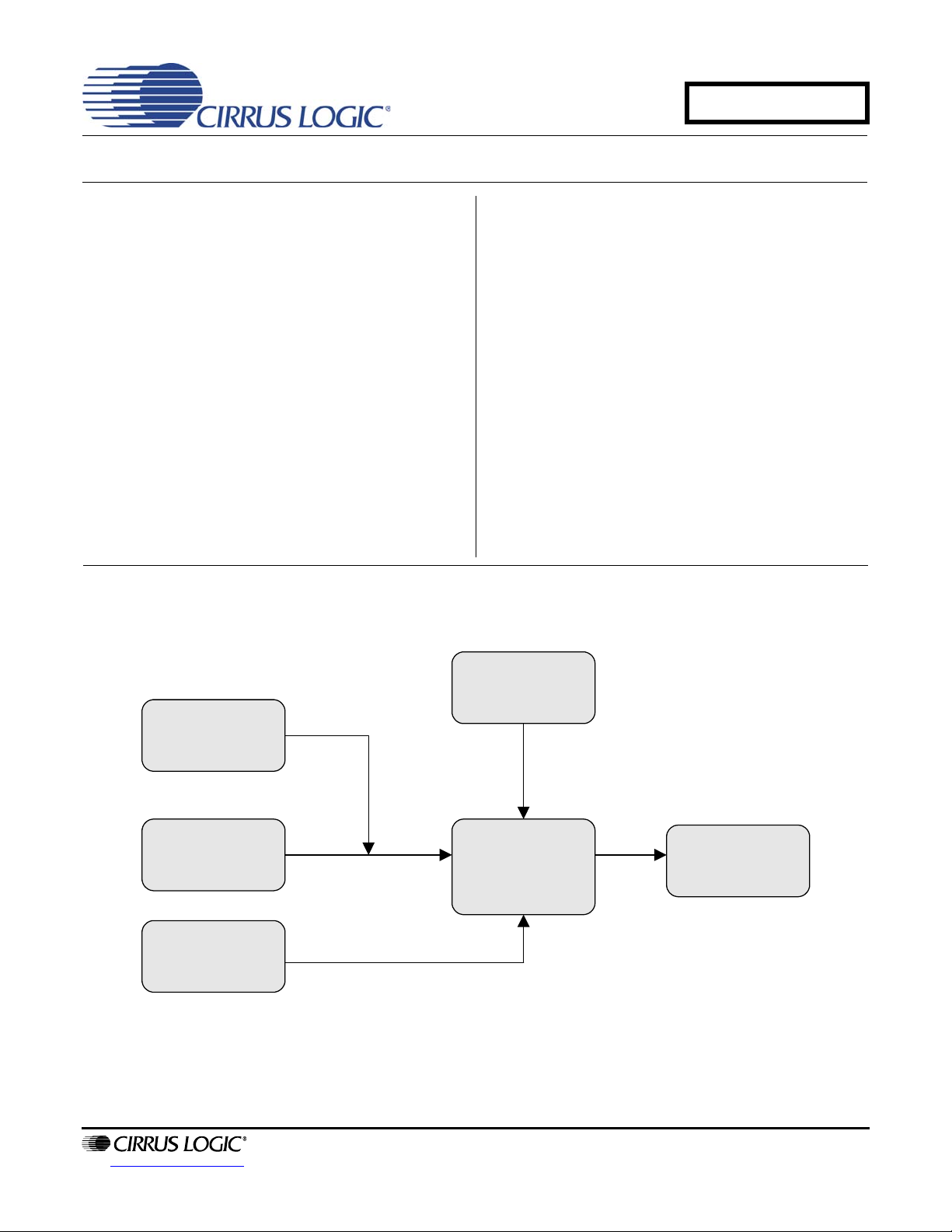
Figure 43.System Block Diagram and SIgnal Flow ................................................................................... 17
Figure 44.CS4365 ..................................................................................................................................... 18
Figure 45.Analog Outputs A1 - B1 ............................................................................................................ 19
Figure 46.Analog Outputs A2 - B2 ............................................................................................................ 20
Figure 47.Analog Outputs A3 - B3 ............................................................................................................ 21
Figure 48.CS8416 S/PDIF Input ............................................................................................................... 22
Figure 49.PCM Input Header and Muxing ................................................................................................. 23
Figure 50.DSD Input Header ..................................................................................................................... 24
Figure 51.Control Input ............................................................................................................................. 25
Figure 52.Power Inputs ............................................................................................................................. 26
Figure 53.Silkscreen Top .......................................................................................................................... 27
Figure 54.Top Side .................................................................................................................................... 28
Figure 55.Bottom Side .............................................................................................................................. 29
LIST OF TABLES
Table 1. System Connections .................................................................................................................... 5
Table 2. CDB4365 Jumper Settings ............................................................................................................6
CDB4365
DS670DB3 3
Page 4

CDB4365
CDB4365 SYSTEM OVERVIEW
The CDB4365 evaluation board is an excellent means of quickly evaluating the CS4365. The CS8416 digital audio
interface receiver provides an easy interface to digi tal audio signal sources including the majority of dig ital audio test
equipment. The evaluation board also allows th e user to supply external PCM or DSD clocks and data through PCB
headers for system development.
The CDB4365 uses the CDB4385 as a base PCB board. For this reason, the re may be additional circui try on board
which is not populated as it has no function for this device.
The CDB4365 schematic has been partitioned into 9 schematics shown in Figure 44 through 52. Each partitioned
schematic is represented in the system diagram shown in Figure Figure 43 on page 17. Notice that the system diagram also includes the interconnections between the partitioned schematics.
1. CS4365 DIGITAL-TO-ANALOG CONVERTER
A description of the CS4365 is included in the CS4365 datasheet.
2. CS8416 DIGITAL AUDIO RECEIVER
The system receives and decodes the standard S/PDIF data format using a CS8416 digital audio receiver
(Figure 48). The outputs of the CS8416 include a serial bit clock, serial data, left-right clock, and a 128/256 Fs master clock. The CS8416 data format is fixed to I²S. The operatio n of the CS8416 and a discu ssion of the digital audio
interface are included in the CS8416 datasheet.
The evaluation board has been designed such that the input can be either optical or coaxial (See Figure 48). However, both inputs cannot be driven simultaneously.
Switch position 7 of S1 sets the output MCLK-to-LRCK ratio of the CS8416. This switch should be set to 256 (closed)
for inputs Fs≤96 kHz and 128 (open) for Fs≥64 kHz. The 8416 must be manually reset using ‘HW RST’ (S2) or
through the software when this switch is changed.
3. INPUT FOR CLOCKS AND DATA
The evaluation board has been designed to allow interfacing to external systems via headers J11 and J7. H eader
J11 allows the evaluation board to accept externally generated PCM clocks and data. The schematic for the
clock/data input is shown in Figure 49. Switch position 6 of S1 selects the source as either CS8416 (o pen) or header
J11 (closed).
Header J7 allows the evaluation board to accept externally generated DSD data and clocks. The sch ematic for the
clock/data input is shown in Figure 50. A synchronous MCLK must still be provided via Header J11. Switch position
8 of S1 selects either PCM (open) or DSD (closed).
Please see the CS4365 datasheet for more info rm at ion .
4. INPUT FOR CONTROL DATA
The evaluation board can be run in either a stand-alon e mode or with a PC. Stand-alone mod e uses the CS4365 in
hardware mode and the mode pins are configured u sing switch positions 1 through 5 of S1. PC mode uses software
to setup the CS4365 through I²C
serial or USB port is attached and the CDB4365 software is running.
®
using the PC’s serial or USB ports. PC mode is automatically selected when the
Header J15 offers the option for external input of RST and SPI
factory to use the on-board microcont roller in conjunction with the supplied software. To use an external control
4 DS670DB3
™/I²C clocks and data. The board is setup from the
Page 5
CDB4365
source, remove the shunts on J15 and place a ribbon cable so the signal lines are on the ce nter row and the grounds
are on the right side. R116 and R119 should be populated with 2-kΩ resistors when using an external I²C source
that does not already provide pull-ups.
5. POWER SUPPLY CIRCUITRY
Power is supplied to the evaluation board by four binding posts: GND, +5V, +12V, and -12V (See Figure 52). The
‘+5V’ terminal supplies VA and the rest of the +5-V circuitry on the board. The +3.3-V circuitry is powered from a
regulator. The +2.5 volts required for VD is also prov ided from an on-boar d regulator. The +5 -V supply should be
set within the recommended values for VA stated in the CS4365 datasheet.
WARNING
cause permanent damage to the device.
: Refer to the CS4365 datasheet for maximum allowable voltage levels. Operation outside this range can
6. GROUNDING AND POWER SUPPLY DECOUPLING
As with any high-performance converter, the CS4365 requires careful attention to power supply and grounding arrangements to optimize performance. Figure 44 details the connections to the CS4365 and Figures 53, 54, and 55
show the component placement and top and bottom layout. The decoupling capacitors are located as close to the
CS4365 as possible. Extensive use of ground plane fill in the evaluation board yields large reductions in radiated
noise.
7. ANALOG OUTPUT FILTERING
The analog output on the CDB4365 has been designed according to the CS4365 datasheet. This output circuit includes an active 2-pole, 50-kHz filter which uses the multiple-feedback topology.
CONNECTOR INPUT/OUTPUT SIGNAL PRESENT
+5V Input + 5 V power
GND Input Ground connection from power supply
+12V Input +12 V positive supply for the on-board filtering
-12V Input -12 V negative supply for the on-board filtering
S/PDIF IN - J9 Input Digital audio interface input via coax
S/PDIF IN - OPT1 Input Digital audio interface input via optical
PCM INPUT - J11 Input Input for master, serial, left/right clocks and serial data
DSD INPUT - J7 Input Input for DSD serial clock and DSD data
OUTA1-B3 Output RCA line level analog outputs
Table 1. System Connections
DS670DB3 5
Page 6
JUMPER /
SWITCH PURPOSE POSITION FUNCTION SELECTED
J15 Selects source of control data
J16 JT AG micro programming - Reserved for factory use only
S2 Resets CS8416 and CS4365 The CS8416 must be reset if switch S1 is changed
CS4365 mode settings M0-M4 1-5
S1
Sets clock source 6
Sets MCLK ratio of CS8416 7
Selects PCM or DSD mode 8 For PCM input set to *Open, for DSD set to Closed
*shunts on Left
shunts removed
*Default Factory Settings
*Control from PC and on-board microcontroller
External control input using center and right columns
Default: M0, M4 open (HI)
M1, M2, M3 closed (LO)
Sets clock source for CS4365
*open = RX(CS8416), closed = EXT
Selects 128x (open) or 256x
output for CS8416
(*closed) MCLK/LRCK ratio
Table 2. CDB4365 Jumper Settings
CDB4365
(J11)
6 DS670DB3
Page 7
CDB4365
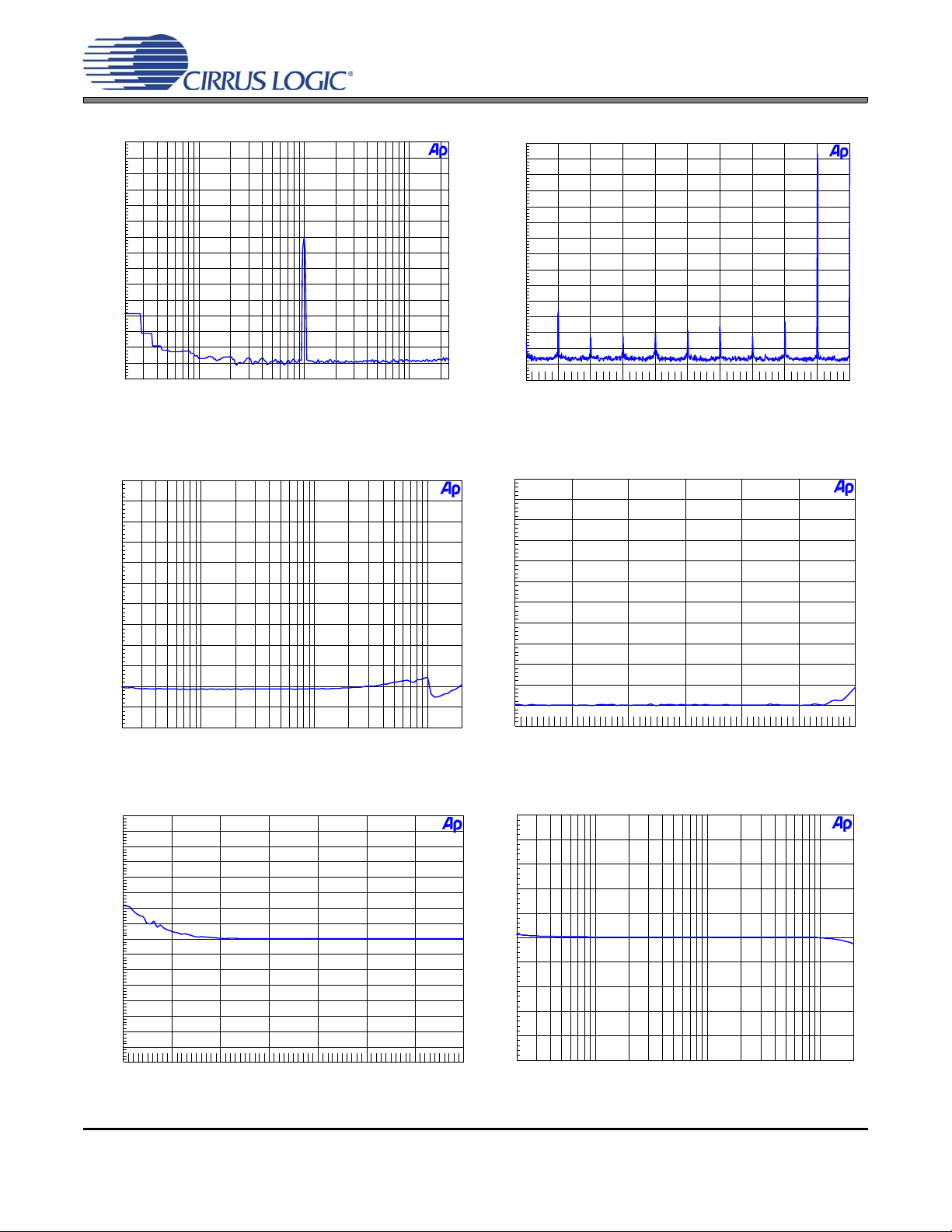
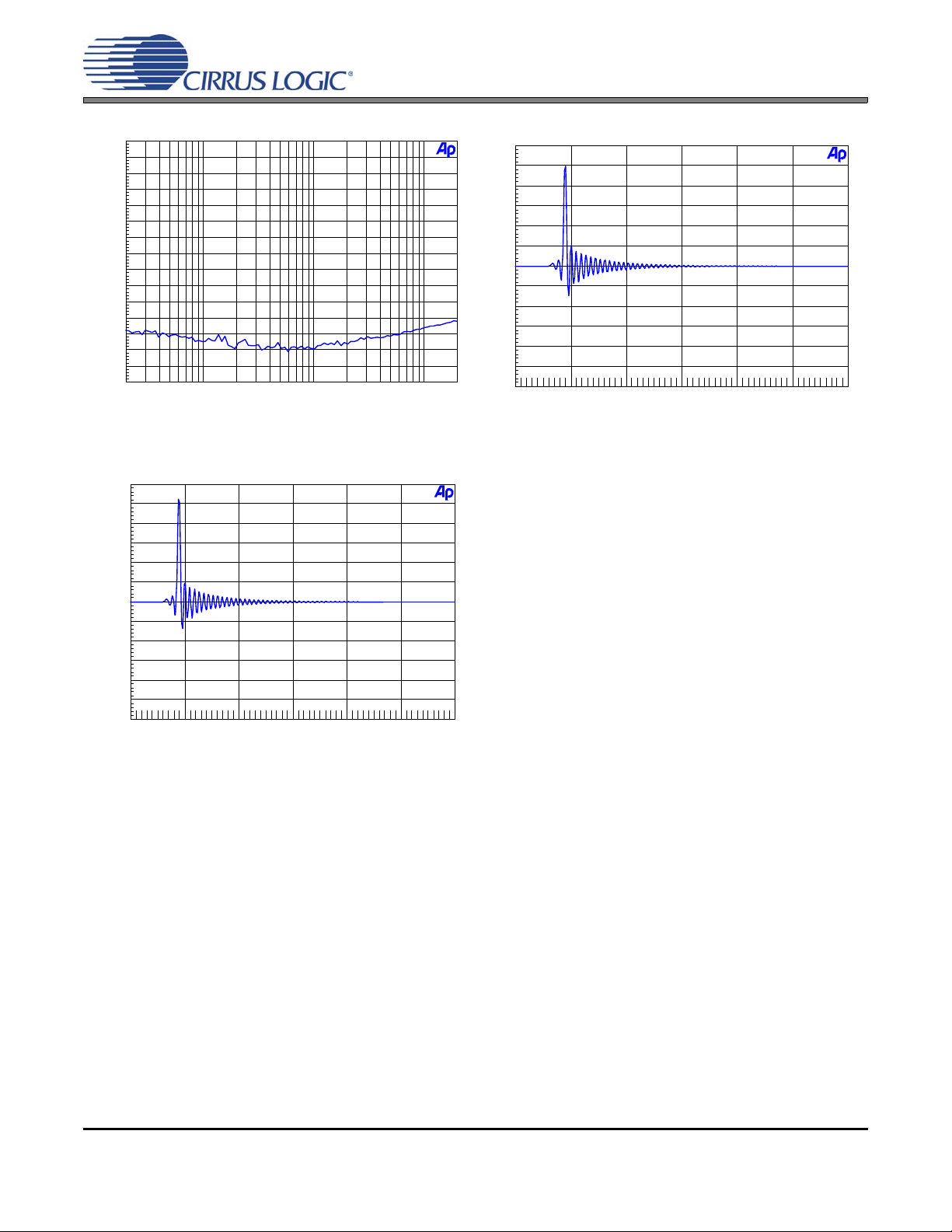
8. PERFORMANCE PLOTS
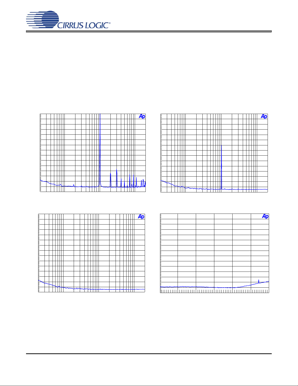
The plots in the following section were acheived using an Audio Precision System 2700 and a ra ndomly chosen production CDB4365. In some cases the performance may be limited by the CDB4365. All measurements were taken
at room temp using the standard AP filter options (20 Hz to 22 kHz) with default board settings and nominal
datasheet voltages applied unless otherwise no te d.
The impulse response plots were taken both pre-and post filtering as the off-chip filter wa s degrading the performance at higher sample rates. The pre-filter impulse response plots were taken directly at the output pins of the
DAC (with the analog filter still connected) to show the effect of the CDB’s analog filtering on the impulse response
(as the analog filtering adds its own signature to the impulse response of the DAC, and in the case of the higher
sampling rates it was band-limiting it).
+0
-10
-20
-30
-40
-50
-60
d
B
-70
r
-80
A
-90
-100
-110
-120
-130
-140
-150
20 20k50 100 200 500 1k 2k 5k 10k
Figure 1. FFT (48 kHz, 0 dB) Figure 2. FFT (48 kHz, -60 dB)
+0
-10
-20
-30
-40
-50
-60
d
-70
B
r
-80
A
-90
-100
-110
-120
-130
-140
-150
20 20k50 100 200 500 1k 2k 5k 10k
Figure 3. FFT (48 kHz, No Input) Figure 4. FFT (48 kHz Out-of-Band, No Input)
Hz
Hz
+0
-10
-20
-30
-40
-50
-60
d
-70
B
r
-80
A
-90
-100
-110
-120
-130
-140
-150
20 20k50 100 200 500 1k 2k 5k 10k
+0
-10
-20
-30
-40
-50
-60
d
B
-70
r
-80
A
-90
-100
-110
-120
-130
-140
-150
20k 120k40k 60k 80k 100k
Hz
Hz
DS670DB3 7
Page 8
CDB4365
+0
-10
-20
-30
-40
-50
-60
d
-70
B
r
-80
A
-90
-100
-110
-120
-130
-140
-150
20 20k50 100 200 500 1k 2k 5k 10k
Hz
+0
-10
-20
-30
-40
-50
-60
d
-70
B
r
-80
A
-90
-100
-110
-120
-130
-140
-150
2k 20k4k 6k 8k 10k 12k 14k 16k 18k
Hz
Figure 5. FFT (48 kHz, -60 dB Wideband) Figure 6. FFT (IMD 48 kHz)
+0
-10
-20
-30
-40
-50
d
B
-60
r
A
-70
-80
-90
-100
-110
-120
20 20k50 100 200 500 1k 2k 5k 10k
Hz
+0
-10
-20
-30
-40
-50
d
B
-60
r
A
-70
-80
-90
-100
-110
-120
-120 +0-100 -80 -60 -40 -20
dBFS
Figure 7. 48 kHz, THD+N vs. Input Freq Figure 8. 48 kHz, THD+N vs. Level
+40
+35
+30
+25
+20
+15
+10
d
+5
B
+0
r
-5
A
-10
-15
-20
-25
-30
-35
-40
-140 +0-120 -100 -80 -60 -40 -20
dBFS
+5
+4
+3
+2
+1
d
B
+0
r
A
-1
-2
-3
-4
-5
20 20k50 100 200 500 1k 2k 5k 10k
Hz
Figure 9. 48 kHz, Fade-to-Noise Linearity Figure 10. 48 kHz, Frequency Response
8 DS670DB3
Page 9
CDB4365
+0
-10
-20
-30
-40
-50
-60
-70
d
B
-80
-90
-100
-110
-120
-130
-140
-150
20 20k50 100 200 500 1k 2k 5k 10k
Hz
Figure 11. 48 kHz, Crosstalk Figure 12. 48 kHz, Impulse Response
3
2.5
2
1.5
1
500m
0
V
-500m
-1
-1.5
-2
-2.5
-3
0 3m500u 1m 1.5m 2m 2.5m
sec
3
2.5
2
1.5
1
500m
0
V
-500m
-1
-1.5
-2
-2.5
-3
0 3m500u 1m 1.5m 2m 2.5m
sec
Figure 13. 48 kHz, Impulse Prefilter
DS670DB3 9
Page 10

CDB4365
Figure 14. 48 kHz Dynamic Range
+0
-10
-20
-30
-40
-50
-60
d
-70
B
r
-80
A
-90
-100
-110
-120
-130
-140
-150
20 20k50 100 200 500 1k 2k 5k 10k
Hz
Figure 15. FFT (96 kHz, 0 dB) Figure 16. FFT (96 kHz, -60 dB)
+0
-10
-20
-30
-40
-50
-60
d
-70
B
r
-80
A
-90
-100
-110
-120
-130
-140
-150
20 20k50 100 200 500 1k 2k 5k 10k
Hz
10 DS670DB3
Page 11

CDB4365
+0
-10
-20
-30
-40
-50
-60
d
-70
B
r
-80
A
-90
-100
-110
-120
-130
-140
-150
20 20k50 100 200 500 1k 2k 5k 10k
Hz
Figure 17. FFT (96 kHz, No Input) Figure 18. FFT (96 kHz Out-of-Band, No Input)
+0
-10
-20
-30
-40
-50
-60
d
B
-70
r
-80
A
-90
-100
-110
-120
-130
-140
-150
20 40k50 100 200 500 1k 2k 5k 10k 20k
Hz
+0
-10
-20
-30
-40
-50
-60
d
B
-70
r
-80
A
-90
-100
-110
-120
-130
-140
-150
+0
-10
-20
-30
-40
-50
-60
d
-70
B
r
-80
A
-90
-100
-110
-120
-130
-140
-150
20k 120k40k 60k 80k 100k
2k 20k4k 6k 8k 10k 12k 14k 16k 18k
Hz
Hz
Figure 19. FFT (96 kHz, -60 db Wideband) Figure 20. FFT (IMD 96 kHz)
+0
-10
-20
-30
-40
-50
d
B
-60
r
A
-70
-80
-90
-100
-110
-120
20 20k50 100 200 500 1k 2k 5k 10k
Hz
+0
-10
-20
-30
-40
-50
d
B
-60
r
A
-70
-80
-90
-100
-110
-120
-120 +0-100 -80 -60 -40 -20
dBFS
Figure 21. 96 kHz, THD+N vs. Input Freq Figure 22. 96 kHz, THD+N vs. Level
DS670DB3 11
Page 12

CDB4365
+40
+35
+30
+25
+20
+15
+10
d
+5
B
+0
r
-5
A
-10
-15
-20
-25
-30
-35
-40
-140 +0-120 -100 -80 -60 -40 -20
dBFS
+5
+4
+3
+2
+1
d
B
+0
r
A
-1
-2
-3
-4
-5
20 20k50 100 200 500 1k 2k 5k 10k
Hz
Figure 23. 96 kHz, Fade-to-Noise Linearity Figure 24. 96 kHz, Frequency Response
+0
-10
-20
-30
-40
-50
-60
-70
d
B
-80
-90
-100
-110
-120
-130
-140
-150
20 20k50 100 200 500 1k 2k 5k 10k
Hz
3
2.5
2
1.5
1
500m
0
V
-500m
-1
-1.5
-2
-2.5
-3
0 1.5m250u 500u 750u 1m 1.25m
sec
Figure 25. 96 kHz, Crosstalk Figure 26. 96 kHz, Impulse Response
3
2.5
2
1.5
1
500m
0
V
-500m
-1
-1.5
-2
-2.5
-3
0 1.5m250u 500u 750u 1m 1.25m
sec
Figure 27. 96 kHz, Impulse Prefilter
12 DS670DB3
Page 13

CDB4365
Figure 28. Dynamic Range 96 kHz
+0
-10
-20
-30
-40
-50
-60
d
-70
B
r
-80
A
-90
-100
-110
-120
-130
-140
-150
20 20k50 100 200 500 1k 2k 5k 10k
Hz
Figure 29. FFT (192 kHz, 0 dB) Figure 30. FFT (192 kHz, -60 dB)
+0
-10
-20
-30
-40
-50
-60
d
-70
B
r
-80
A
-90
-100
-110
-120
-130
-140
-150
20 20k50 100 200 500 1k 2k 5k 10k
Hz
DS670DB3 13
Page 14

CDB4365
+0
-10
-20
-30
-40
-50
-60
d
-70
B
r
-80
A
-90
-100
-110
-120
-130
-140
-150
20 20k50 100 200 500 1k 2k 5k 10k
Hz
+0
-10
-20
-30
-40
-50
-60
d
-70
B
r
-80
A
-90
-100
-110
-120
-130
-140
-150
20k 120k40k 60k 80k 100k
Hz
Figure 31. FFT (192 kHz, No Input) Figure 32. FFT (192 kHz Out-of-Band, No Input)
+0
-10
-20
-30
-40
-50
-60
d
B
-70
r
-80
A
-90
-100
-110
-120
-130
-140
-150
20 90k50 100 200 500 1k 2k 5k 10k 20k 50k
Hz
+0
-10
-20
-30
-40
-50
-60
d
-70
B
r
-80
A
-90
-100
-110
-120
-130
-140
-150
2k 20k4k 6k 8k 10k 12k 14k 16k 18k
Hz
Figure 33. FFT (192 kHz, -60 dB Wideband) Figure 34. FFT (IMD 192 kHz)
+0
-10
-20
-30
-40
-50
d
B
-60
r
A
-70
-80
-90
-100
-110
-120
20 20k50 100 200 500 1k 2k 5k 10k
Hz
+0
-10
-20
-30
-40
-50
d
B
-60
r
A
-70
-80
-90
-100
-110
-120
-120 +0-100 -80 -60 -40 -20
dBFS
Figure 35. 192 kHz, THD+N vs. Input Freq Figure 36. 192 kHz, THD+N vs. Level
14 DS670DB3
Page 15

CDB4365
+40
+35
+30
+25
+20
+15
+10
d
+5
B
+0
r
-5
A
-10
-15
-20
-25
-30
-35
-40
-140 +0-120 -100 -80 -60 -40 -20
dBFS
+5
+4
+3
+2
+1
d
B
+0
r
A
-1
-2
-3
-4
-5
20 20k50 100 200 500 1k 2k 5k 10k
Hz
Figure 37. 192 kHz, Fade-to-Noise Linearity Figure 38. 192 kHz, Frequency Response
+0
-10
-20
-30
-40
-50
-60
-70
d
B
-80
-90
-100
-110
-120
-130
-140
-150
20 20k50 100 200 500 1k 2k 5k 10k
Hz
3
2.5
2
1.5
1
500m
0
V
-500m
-1
-1.5
-2
-2.5
-3
0 600u200u 400u
sec
Figure 39. 192 kHz, Crosstalk Figure 40. 192 kHz, Impulse Response
3
2.5
2
1.5
1
500m
0
V
-500m
-1
-1.5
-2
-2.5
-3
0 600u200u 400u
sec
Figure 41. 192 kHz, Impulse Prefilter
DS670DB3 15
Page 16

CDB4365
Figure 42. Dynamic Range 192 kHz
16 DS670DB3
Page 17

DS670DB3 17
9. CDB4365 SCHEMATICS
Serial Control Port
Figure 51 on page 25
Power
Figure 52 on page 26
PCM HEADER
Figure 49 on
page 23
CS8416
S/PDIF
Input
Figure 48 on
page 22
PCM Clocks/Data
PCM Clocks/Data
PCM mux
Figure 49 on
page 23
select
PCM source
6
S
841
C
clock setting
PCM Clocks/Data
)
s
alone
mode
switche
-
4
- M
0
for
stand
M
(
Hardware Control
Switches
Figure 51 on page 25
I2C/SPI Hea d er
Differential to Single-Ended
Analog Outputs
2
2
A1, B1
Figure 45 on page 19
A2, B2
Figure 46 on page 20
CS4365
2
DSD clk_enable
enable
DSD input
Figure 50 on page 24
a
Dat
DSD Clocks/
DSD HEADER
A3, B3
Figure 47 on page 21
CDB4365
Figure 43. System Block Diagram and SIgnal Flow
Page 18

18 DS670DB3
Figure 44. CS4365
CDB4365
Page 19

CDB4365
Figure 45. Analog Outputs A1 - B1
DS670DB3 19
Page 20

CDB4365
Figure 46. Analog Outputs A2 - B2
20 DS670DB3
Page 21

CDB4365
Figure 47. Analog Outputs A3 - B3
DS670DB3 21
Page 22

22 DS670DB3
Figure 48. CS8416 S/PDIF Input
CDB4365
Page 23

DS670DB3 23
Figure 49. PCM Input Header and Muxing
CDB4365
Page 24

24 DS670DB3
Figure 50. DSD Input Header
CDB4365
Page 25

DS670DB3 25
Figure 51. Control Input
CDB4365
Page 26

26 DS670DB3
Figure 52. Power Inputs
CDB4365
Page 27

DS670DB3 27
Figure 53. Silkscreen Top
CDB4365
Page 28

28 DS670DB3
Figure 54. Top Side
CDB4365
Page 29

DS670DB3 29
Figure 55. Bottom Side
CDB4365
Page 30

10.REVISION HISTORY
Release Changes
DB1 Initial Release
DB2 Added Performance Plots
DB3 Added USB support to Section 4. Input for Control Data
CDB4365
Contacting Cirrus Logic Support
For all product questions and inquiries, contact a Cirrus Logic Sales Representative.
To find the one nearest to you, go to www.cirrus.com.
IMPORTANT NOTICE
Cirrus Logic, Inc. and it s subsidiaries ("Cirrus") believe that the information contained in this document is accurate and reliable. However, the information is subject
to change without noti ce and is provided " AS IS" withou t warrant y of any ki nd (expr ess or impli ed). Cust omers are ad vised to ob tain the latest version of relevant
information to verify, before placin g or ders, tha t in form ation be ing r elied o n is cu rre nt an d com ple te. All prod ucts a re so ld subject to the terms and conditions of sale
supplied at the time of order acknow ledgment, includ ing those pertaini ng to warranty, indem nification, and limitation of liability . No respons ibility is assume d by Cirrus
for the use of this information, including use of this information as the basis for manufacture or sale of any items, or for infringement of patents or other rights of third
parties. This document is the property of Cirrus and by furnishing this information, Cirrus grants no license, express or implied under any patents, mask work rights,
copyrights, trademarks, trade secrets or other intellectual property rights. Cirrus owns the copyrights associated with the information contained herein and gives consent for copies to be made of the inform atio n o nl y for use with in yo ur or ga ni zatio n with respect to Cirrus integrated circuits or other products of Cirrus. This consent
does not extend to other copying such as copying for ge neral distribution, advertising or promotional purposes, or for creating any work for resale .
CERTAIN APPLICATIONS USING SEMICONDUCTOR PRODUCTS MAY INVOLVE POTENTIAL RISKS OF DEATH, PERSONAL INJURY, OR SEVERE PROPERTY OR ENVIRONMENTAL DAM AGE (“CRITICAL APPLICATIONS”). CIRRUS PRODUCTS ARE NOT DESIGNED, AUTHORIZED OR WARRANTED FOR USE
IN PRODUCTS SURGICALLY IMPLANTED INTO THE BODY, AUTOMOTIVE SAFETY OR SECURITY DEVICES, LIFE SUPPORT PRODUCTS OR OTHER CRITICAL APPLICATIONS. INCLUSION OF CIRRUS PRODUCTS IN SUCH APPLICATIONS IS UNDERSTOOD TO BE FULLY AT THE CUSTOMER’S RISK AND
CIRRUS DISCLAIMS AND MAKES NO WARRANTY, EXPRESS, STATUTORY OR IMPLIED, INCLUDING THE IMPLIED WARRANTIES OF MERCHANTABILITY
AND FITNESS FOR PARTICULAR PURPOSE, WITH REGARD TO ANY CIRRUS PRODUCT THAT IS USED IN SUCH A MANNER. IF THE CUSTOMER OR
CUSTOMER’S CUSTOMER USES OR PERMITS THE USE OF CIRRUS PRODUCTS IN CRITICAL APPLICATIONS, CUSTOMER AGREES, BY SUCH U SE, TO
FULLY INDEMNIFY CIRRUS, ITS OFFICERS, DIRECTORS, EMPLOYEES, DISTRIBUTORS AND OTHER AGEN T S FR OM ANY AND ALL LIABILITY, INCLUDING ATTORNEYS’ FEES AND COSTS, THAT MAY RESULT FROM OR ARISE IN CONNECTION WITH THESE USES.
Cirrus Logic, Cirrus, and the Cirrus Logic logo design s are trad em ark s of Cirrus Logi c, Inc. All other b rand and p rodu ct nam es in this d ocum ent ma y be trad em arks
or service marks of their respective owners.
DSD is a registered trademark of Sony Kabushiki Kaisha TA Sony Company.
I²C is a registered trademark of Philips Semiconductor.
SPI is a trademark of Motorola, Inc.
30 DS670DB3
 Loading...