Page 1

CDB4360
Evaluation Board for CS4360 Rev. B
Features
l Demonstrates recommended layout and
grounding arrangements
l CS8414 receives AES/EBU, S/PDIF, and
EIAJ-340 Compatible Digital Audio
l Requires only a digital signal source and
power supplies for a complete Digital-toAnalog-Converter system
Description
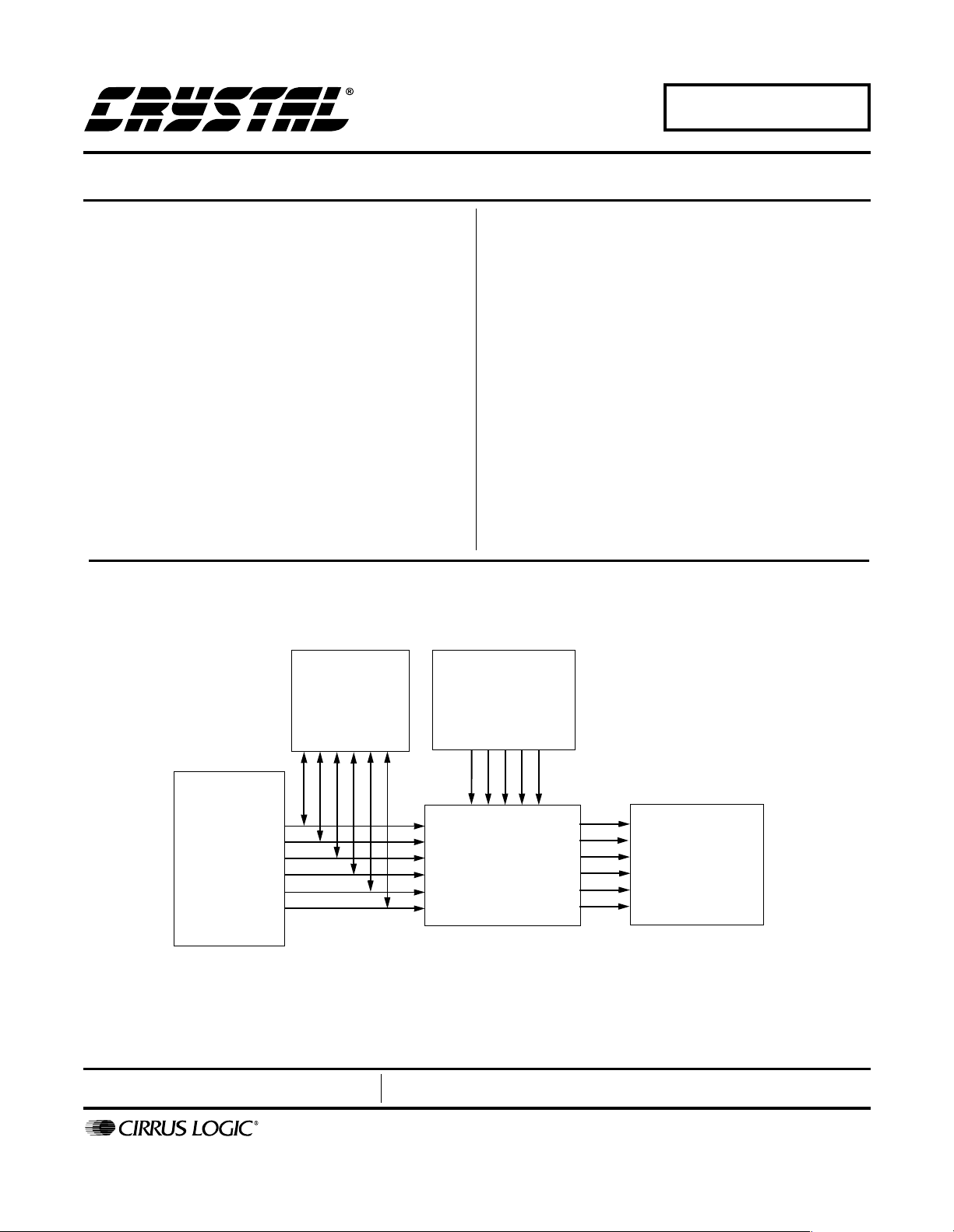
The CDB4360 evaluation board is an excellent means
for quickly evaluating the CS4360 24-bit, stereo D/A converter. Evaluation requires an analog signal analyzer, a
digital signal source, a PC for controlling the CS4360 (for
control port mode only) and a power supply. Line outputs are provided via RCA phono jacks.
The CS8414 digital audio receiver I.C. provides the system timing necessary to operate the Digital-to-Analog
converter and will accept AES/EBU, S/PDIF, and EIAJ340 compatible audio data. The evaluation board may
also be configured to accept external timing and data
signals for operation in a user application during system
development.
ORDERING INFORMATION
CDB4360 Evaluation Board
I/O for
Clocks
and Data
CS8414
Digital
Audio
Interface
Preliminary Product Information
Control Port
Six
CS4360
Line Level
Outputs
This document contains information for a new product.
Cirrus Logic reserves the right to modify this product without notice.
P.O. Box 17847, Austin, Texas 78760
(512) 445 7222 FAX: (512) 445 7581
http://www.cirrus.com
Copyright Cirrus Logic, Inc. 2001
(All Rights Reserved)
AUG ‘01
DS517DB2
1
Page 2

TABLE OF CONTENTS
1. CDB4360 SYSTEM OVERVIEW .................................................................... 3
2. CS4360 DIGITAL TO ANALOG CONVERTER .............................................. 3
3. CS8414 DIGITAL AUDIO RECEIVER ............................................................ 3
4. INPUT/OUTPUT FOR CLOCKS AND DATA ................................................. 3
5. POWER SUPPLY CIRCUITRY ....................................................................... 3
6. GROUNDING AND POWER SUPPLY DECOUPLING .................................. 3
7. CONTROL PORT SOFTWARE ...................................................................... 3
8. ERRATA ......................................................................................................... 4
LIST OF FIGURES
Figure 1. System Block Diagram and Signal Flow .......................................................................... 5
Figure 2. CS4360 ............................................................................................................................ 6
Figure 3. CS8414 - Digital Audio Receiver...................................................................................... 7
Figure 4. Control Port Interface and Level Shifters ......................................................................... 8
Figure 5. Digital Audio Inputs and Level Shifters ............................................................................ 9
Figure 6. Line Level Outputs (AOUTA1, AOUTB1) ....................................................................... 10
Figure 7. Line Level Outputs (AOUTA2, AOUTB2) ....................................................................... 11
Figure 8. Line Level Outputs (AOUTA3, AOUTB3) ....................................................................... 12
Figure 9. Power Supplies .............................................................................................................. 13
Figure 10. Silkscreen Top ............................................................................................................. 14
Figure 11. Top Side ....................................................................................................................... 15
Figure 12. Bottom Side.................................................................................................................. 16
CDB4360
Contacting Cirrus Logic Support
For a complete listing of Direct Sales, Distributor, and Sales Representative contacts, visit the Cirrus Logic web site at:
http://www.cirrus.com/corporate/contacts/
Preliminary product information describes products which are in production, but for which full characterization data is not yet available. Advance product information describes products which are in development and subject to development changes. Cirrus Logic, Inc. has made best efforts to ensure that the information
contained in this document is accurate and reliable. However, the information is subject to change without notice and is provided “AS IS” without warranty of
any kind (express or implied). No responsibility is assumed by Cirrus Logic, Inc. for the use of this information, nor for infringements of patents or other rights
of third parties. This document is the property of Cirrus Logic, Inc. and implies no license under patents, copyrights, trademarks, or trade secrets. No part of
this publication may be copied, reproduced, stored in a retrieval system, or transmitted, in any form or by any means (electronic, mechanical, photographic, or
otherwise) without the prior written consent of Cirrus Logic, Inc. Items from any Cirrus Logic website or disk may be printed for use by the user. However, no
part of the printout or electronic files may be copied, reproduced, stored in a retrieval system, or transmitted, in any form or by any means (electronic, mechanical,
photographic, or otherwise) without the prior written consent of Cirrus Logic, Inc.Furthermore, no part of this publication may be used as a basis for manufacture
or sale of any items without the prior written consent of Cirrus Logic, Inc. The names of products of Cirrus Logic, Inc. or other vendors and suppliers appearing
in this document may be trademarks or service marks of their respective owners which may be registered in some jurisdictions. A list of Cirrus Logic, Inc. trademarks and service marks can be found at http://www.cirrus.com.
2 DS517DB2
Page 3

CDB4360
1. CDB4360 SYSTEM OVERVIEW
The CDB4360 evaluation board is an excellent
means of quickly evaluating the CS4360. The
CS8414 digital audio interface receiver provides an
easy interface to digital audio signal sources including the majority of digital audio test equipment. The evaluation board also allows the user to
supply clocks and data through a 10-pin header for
system development.
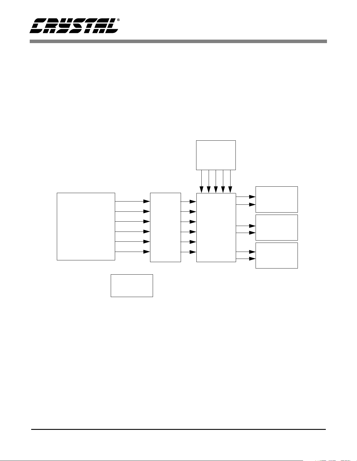
The CDB4360 schematic has been partitioned into
8 schematics shown in Figures 2 through 9. Each
partitioned schematic is represented in the system
diagram shown in Figure 1. Notice that the system
diagram also includes the interconnections between the partitioned schematics.
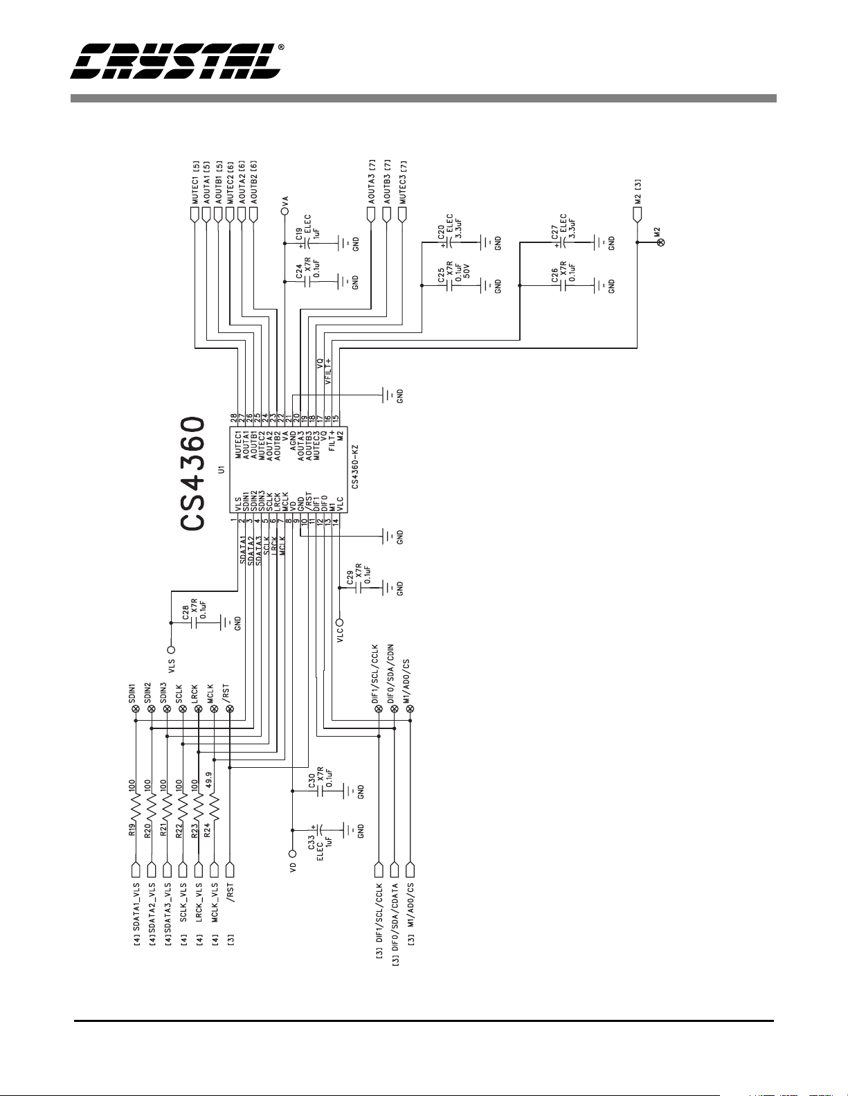
2. CS4360 DIGITAL TO ANALOG CONVERTER
A description of the CS4360 is included in the
CS4360 datasheet.
3. CS8414 DIGITAL AUDIO RECEIVER
accept externally generated clocks and data. The
schematic for the clock/data I/O is shown in
Figure 5.
5. POWER SUPPLY CIRCUITRY
Power is supplied to the evaluation board by six
binding posts (GND, +5 V, VLC, VLS, VD, and
VA), see Figure 9. The +5 V input supplies power
to the +5 Volt digital circuitry (VD_+5), while the
VLC input supplies power to the Voltage Level
Converters for the control port interface and the
CS4360 VLC pin. The VLS input supplies power
to the Voltage Level Converters for the serial audio
port interface and the CS4360 VLS pin. VA and
VD supply power to the CS4360. For ease of use,
it is possible to connect VLC, VLS, VD, and VA to
the same supply.
WARNING: VA and VD must be between +2.7V
and +5.5V. VLC and VLS must be between +1.7 V
and +5.5 V. Operation outside of this range can
cause permanent damage to the device. See the
CS4360 datasheet for more details.
The system receives and decodes the standard
S/PDIF data format using a CS8414 Digital Audio
Receiver, Figure 3. The outputs of the CS8414 include a serial bit clock, serial data, left-right clock
(FSYNC), and a 256 x Fs master clock. The operation of the CS8414 and a discussion of the digital
audio interface are included in the CS8414
datasheet.
The evaluation board has been designed such that
the input can be either optical or coax, see Figure 3.
However, both inputs cannot be driven simultaneously.
The CS8414 data format is hard-wired to I2S.
4. INPUT/OUTPUT FOR CLOCKS AND
DATA
The evaluation board has been designed to allow
interfacing to external systems via the 10-pin header, J24. This header allows the evaluation board to
6. GROUNDING AND POWER SUPPLY DECOUPLING
The CS4360 requires careful attention to power
supply and grounding arrangements to optimize
performance. Figure 2 details the power distribution used on this board. The decoupling capacitors
are located as close to the CS4360 as possible. Extensive use of ground plane fill on both the analog
and digital sections of the evaluation board yields
large reductions in radiated noise. See Figures 1012 for the CDB4360 PCB layout artwork.
7. CONTROL PORT SOFTWARE
The CDB4360 is shipped with Windows based
software for interfacing with the CS4360 control
port via the parallel connector, J28. The software
can be used to communicate with the CS4360 in
SPI or Two Wire mode. Note: J18-J21 must be set
appropriately for control port mode operation.
DS517DB2 3
Page 4

CDB4360
8. ERRATA
should be labeled “SA”. The labeling is correct in
the schematics.
CDB4360 Revision A.0
The CDB4360 revision A.0 has the following errata. The silkscreen for J18 is reversed. The right position should be labeled “CP” and the left position
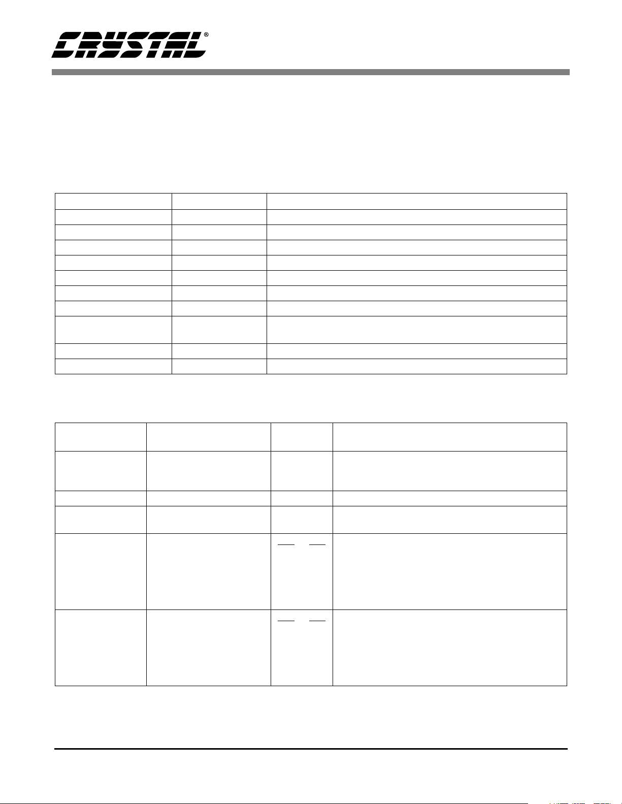
CONNECTOR INPUT/OUTPUT SIGNAL PRESENT
+5 V Input + 5 Volt power
VA, VD Input + 3.0 Volt to + 5.0 Volt power for the CS4360
VLC, VLS Input +1.8 Volt to +5.0 Volt power for the Level Shifters and the CS4360
GND Input Ground connection from power supply
Coax Input Input Digital audio interface input via coax
Optical Input Input Digital audio interface input via optical
J24 Input/Output I/O for master, serial, left/right clocks and serial data
Parallel Port Input/Output Serial connection to PC for SPI and Two Wire mode control port
signals
J17 Input/Output I/O for SPI and Two Wire mode control port signals
AOUTAx, AOUTBx Output Line outputs
Table 1. System Connections
CDB4360 Revision B.0
The CDB4360 revision B.0 has no Errata.
JUMPER/
SWITCH PURPOSE POSITION FUNCTION SELECTED
S1 (DIP SW) Enable/Disable the
CS8414
Reset (S2) Resets the CDB4360
†
J18
J19, J20 Interface Format J19
J22, J21 Mode Select J22
Notes: *Default factory settings
†See Errata section
Selects Stand-Alone or
Control Port mode
*CLOSED
OPEN
CP
*SA
J20
LO
*LO
*LO
LO
HI
HI
HI
HI
HI
HI
LO
*HI
LO
HI
HI
J21
*LO
HI
LO
HI
HI
CS8414 is enabled (J24 is an output)
Disabled (External Clocks and Data are input via
J24)
Control Port Mode selected
Stand-Alone mode selected
Stand-Alone Mode, Left Justified format
Stand-Alone Mode, I2S format
Stand-Alone Mode, Right Justified, 16-bit format
Stand-Alone Mode, Right Justified, 24-bit format
Control Port Mode setting
Stand-Alone Mode, Single Speed, no De-Emphasis
Stand-Alone Mode, Single Speed, De-Emphasis
Stand-Alone Mode, Double Speed
Stand-Alone Mode, Quad Speed
Control Port Mode setting
Table 2. CDB4360 Jumper and Switch settings
4 DS517DB2
Page 5

CDB4360
Control
Port
Figure 4
Line Level
Output
Figure 6
Line Level
Output
Figure 7
Line Level
Output
Figure 8
CS8414
Digital & Audio
Receiver
Figure 3
I/O for
Clock
and
Data
&
Level
Shifter
Figure 5
CS4360
Figure 2
Power
Figure 9
Figure 1. System Block Diagram and Signa
DS517DB2 5
l Flow
Page 6

CDB4360
Figure 2. CS4360
6 DS517DB2
Page 7

CDB4360
Figure 3. CS8414 - Digital Audio Receiver
DS517DB2 7
Page 8

CDB4360
Figure 4. Control Port Interface and Level Shifters
8 DS517DB2
Page 9

CDB4360
Figure 5. Digital Audio Inputs and Level Shifters
DS517DB2 9
Page 10

CDB4360
Figure 6. Line Level Outputs (AOUTA1, AOUTB1)
10 DS517DB2
Page 11

CDB4360
Figure 7. Line Level Outputs (AOUTA2, AOUTB2)
DS517DB2 11
Page 12

CDB4360
Figure 8. Line Level Outputs (AOUTA3, AOUTB3)
12 DS517DB2
Page 13

CDB4360
Figure 9. Power Supplies
DS517DB2 13
Page 14

CDB4360
Figure 10. Silkscreen Top
14 DS517DB2
Page 15

CDB4360
Figure 11. Top Side
DS517DB2 15
Page 16

CDB4360
Figure 12. Bottom Side
16 DS517DB2
Page 17

• Notes •
Page 18

 Loading...