

Page 1
Evaluation Board for the CS4354
CDB4354
Features
Requires Only a Digital Signal Source and a
+5 V Power Supply for a Complete Digital-toAnalog Converter System
Demonstrates Recommended Layout and
Grounding Arrangements
CS8416 Receives S/PDIF, & EIAJ-340-
Compatible Digital Audio
Header for External PCM Audio
Single-ended Stereo Analog Outputs
Power and S/PDIF Error Indicator LEDs
Hardware Controls: +5 V/3.3 V select for VL,
De-emphasis select
Current Sense Resistors for CS4354 Supplies
(VA and VL)
Description
The CDB4354 evaluation board is a dedicated platform
designed to facilitate the evaluation of the CS4354 24bit, stereo D/A converter. Evaluation requires an analog
signal analyzer, a digital signal source, and a +5 V power supply. Analog line-level outputs are provided via
RCA phono jacks.
The CS8416 digital audio receiver IC provides the system timing necessary to operate the Digital-to-Analog
converter and will accept S/PDIF and EIAJ-340-compatible audio data. The evaluation board may also be
configured to accept external timing and data signals for
operation in a custom user application during system
development.
To accommodate various system configurations, several hardware controls and resistor population options are
provided. Current sense resistors allow for easy power
calculations during system development.
ORDERING INFORMATION
CDB4354 Evaluation Board
Optical S/PDIF
Input
Coaxial S/PDIF
Input
Direct External
Input
http://www.cirrus.com
Hardware Controls
CS8416
Manual
Reset
CS8416
S/PDIF
Receiver
Clocks &
Serial
Audio
Data
+5V Input, +3.3V Regulator
VL Select:
5V or 3.3V
Clocks &
Data
Selection
(Headers)
Copyright Cirrus Logic, Inc. 2010
(All Rights Reserved)
Power:
Serial
Audio
Clocks &
Data
De-emphasis
CS4354
CS4354
Select
Indicator LEDs
+5V power
+3.3V pow er
VL power
S/P DIF E rror
AOUTA
Filter
Analog
Outputs
AOUTB
Filter
JULY '10
DS895DB1
Page 2

TABLE OF CONTENTS
1. THE CDB4354 SYSTEM ........................................................................................................................ 3
2. BOARD CONNECTIONS AND SETTINGS ............................................................................................ 5
3. SCHEMATICS AND LAYOUT ........................................................................................................... 7
4. REVISION HISTORY ........................................................................................................................... 11
LIST OF FIGURES
Figure 1. CDB4354 Factory Default Jumper Settings ................................................................................. 6
Figure 2. System Block Diagram and Signal Flow ...................................................................................... 7
Figure 3. CS8416 and CS4354 ................................................................................................................... 8
Figure 4. Power ........................................................................................................................................... 9
Figure 5. Silkscreen Top ........................................................................................................................... 10
Figure 6. Top Side ..................................................................................................................................... 10
Figure 6. Top Side ..................................................................................................................................... 10
Figure 7. Bottom Side ............................................................................................................................... 10
LIST OF TABLES
Table 1. System Connections .................................................................................................................... 5
Table 2. CDB4354 Jumper Pin Block Settings ............................................................................................ 5
Table 3. LED Information ............................................................................................................................ 5
CDB4354
2 DS895DB1
Page 3

CDB4354
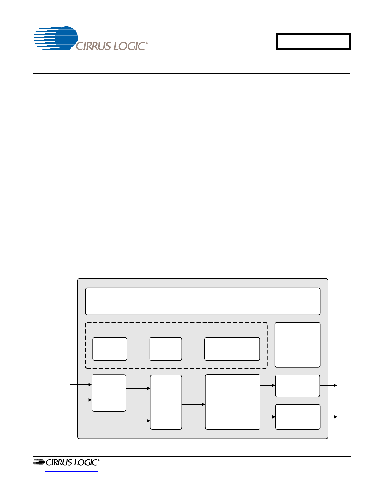
1. THE CDB4354 SYSTEM
The CDB4354 is a dedicated platform for evaluating the CS4354. The CS8416 digital audio interface receiver provides an easy interface to digital audio signal sources, including the majority of digital audio test equipment. The
evaluation board also allows the user to supply external PCM clocks and data directly to the CS4354 through a header block for system development. In addition, hardware controls are available to test board and CS4354-specific features.
The CDB4354 system block diagram and signal flow is shown in Figure 2. The CDB4354 schematics are shown in
Figures 3 and 4.
1.1 CS4354 Digital-to-Analog Converter
The CS4354 is a 24-bit, 2 V
ed) dynamic range. A complete description of the CS4354 is included in the CS4354 datasheet.
ground-centered output digital-to-analog converter with 101 dB (A-weight-
RMS
1.2 CS8416 Digital Audio Receiver
The system receives and decodes the standard S/PDIF data format using a CS8416 Digital Audio Receiver.
The outputs of the CS8416 are standard PCM clocks and data: 256 Fs master clock, serial bit clock, leftright clock, and serial data. The operation of the CS8416 and a discussion of the digital audio interface is
included in the CS8416 datasheet.
The evaluation board has been designed such that the active input can be either optical (OPT1) or coaxial
(J16). However, both inputs cannot be driven simultaneously.
1.3 Input for Serial Audio Clocks and Data
By default, the shunts on header block J6 are placed across columns 1 and 2, marked “SPDIF_RX”, which
routes the serial audio clocks and data from the CS8416 to the CS4354. This makes the S/PDIF inputs on
the evaluation board the default inputs. However, the user may remove these shunts and connect an external source to columns 2 and 3 of header block J6, marked “EXT,” via a ribbon cable. Column 3 of J6 are
GND pins to maintain signal ground integrity when using external clocks and data.
Signals input to header J6 must be at the same voltage level as the VL supply on the evaluation board.
When using the S/PDIF inputs on the evaluation board with columns 1 and 2 of J6 shunted, this requirement
is always met and thus requires no precaution on the user’s part.
Please see the CS4354 datasheet for more information on clocking data into the CS4354.
Note: If the VL supply is set to a low voltage level (VL<1.8 V), termination resistors may need to be added
to the J6 header signals to match the source and transmission-line impedances that are driving the
header. This may be accomplished by soldering resistors across the rows of J6 on the back of the
evaluation board.
1.4 Power Supply Circuitry
Power is supplied to the evaluation board by two binding posts, J2 (+5 V) and GND. The allowable input
voltage range for J2 is 4.75 V to 5.25 V. The VA supply for the CS4354 is sourced directly from the +5 V
supply. The VL supply can be sourced from either the +5 V supply or a +3.3 V regulated version, selected
using J12. Furthermore, the user can have full control over the VL supply voltage by removing the shunt
from J12, and connecting an external supply to pin 2 of J12. When using the S/PDIF inputs, the allowable
voltage range for pin 2 of J12 is 3.13 V to 5.25 V. When using external serial audio clocks and data, the
allowable voltage range for pin 2 of J12 is 1.4 V to 5.25 V.
DS895DB1 3
Page 4

Power consumption of the CS4354 can be calculated with the measured voltage drop at J4 and J5 when
the shunts are removed.
WARNING: Refer to the CS4354 datasheet for maximum allowable voltages levels. Operation outside of
this range can cause permanent damage to the device.
1.5 Grounding and Power Supply Decoupling
As with any high-performance converter, the CS4354 requires careful attention to power supply and grounding arrangements to optimize performance. Figure 3 details the connections to the CS4354 and Figures 5,
6, and 7 show the component placement and top and bottom layout. The charge-pump and decoupling ca-
pacitors are located as close to the CS4354 as possible.
1.6 Hardware Control
The CDB4354 includes several shuntable jumper pin blocks to test CS4354-specific and board features,
such as:
• De-emphasis and Internal Serial Clock select for the CS4354
• Manual reset for the CS8416
• +5 V/+3.3 V select for the VL supply
Please use Table 2 as a guide to the possible configurations for these controls.
CDB4354
1.7 Analog Output Filtering
The analog output filter circuitry on the CDB4354 has been designed according to the CS4354 datasheet.
This circuit is a first order resistor-capacitor low pass filter with values 470 /2.2 nF, respectively, which sets
the -3 dB pole at 154 kHz. The resulting filter keeps signal attenuation below 0.1 dB at 20 kHz while providing sufficient filtering for noise outside the audio band.
4 DS895DB1
Page 5

2. BOARD CONNECTIONS AND SETTINGS
Board connections and settings are shown in Table 1 and Table 2 below.
CONNECTOR INPUT/OUTPUT SIGNAL PRESENT
+5 V - J2 Input +3.3 V power for the evaluation board
GND - J1 Input Ground connection from power supply
S/PDIF INPUT - J16 Input Digital audio interface input via coaxial cable
S/PDIF INPUT - OPT1 Input Digital audio interface input via optical cable
Serial Audio Header Pin
Block - J6
AOUTA - J7
AOUTB - J8
Input
Output
Input for master, serial, left/right clocks and serial data (MCLK, SCLK,
LRCK, and SDIN) - direct to CS4354
RCA line-level analog outputs
Table 1. System Connections
CDB4354
JUMPER PIN
BLOCK
J12
J4 Current measure for VL
J5 Current measure for VA
J9 CS8416 Manual Reset
J3
PURPOSE POSITION FUNCTION SELECTED
Selects source of voltage
for the VL supply
CS4354 De-emphasis and
Internal Serial Clock Mode
Select
Table 2. CDB4354 Jumper Pin Block Settings
pins [1, 2] shunted
*pins [2,3] shunted
not shunted
*shunted
not shunted
*shunted
not shunted
shunted
*not shunted
pins [1, 2] shunted
*pins [2, 3] shunted
not shunted
LED FUNCTION
+3.3V - D1
+5V - D2 LED is illuminated when the +5 V supply is on
VL - D4 LED is illuminated when the VL supply is on (either by the onboard +3.3 V, +5 V or external supply)
S/PDIF - D10
LED is illuminated when the +3.3 V supply is on (+3.3V is derived from the +5V supply by an on-board
regulator)
LED is illuminated when the CS8416 reports a Receiver Error. See the CS8416 datasheet for a full
description of the error reporting functionality.
Voltage source is +5 V
Voltage source is +3.3 V
Voltage source is pin 2 of J12
When shunt is removed, the voltage can be measured
across a fixed resistance R2 to determine current.
When shunt is removed, the voltage can be measured
across a fixed resistance R3 to determine current.
CS8416 is held in reset as long as J9 is shunted
CS8416 uses the on-board automatic reset
Internal Serial Clock Mode, De-emphasis enabled
External Serial Clock Mode, De-emphasis disabled
Internal Serial Clock Mode, De-emphasis disabled
Table 3. LED Information
Note: All settings denoted by an asterisk (*) are the Factory Default Settings.
DS895DB1 5
Page 6

CDB4354
Figure 1. CDB4354 Factory Default Jumper Settings
6 DS895DB1
Page 7

DS895DB1 7
CS4354
CS8416
S/PDIF
Receiver
Serial
Audio
Clocks &
Data
Analog
Outputs
Clocks &
Data
Selection
(Headers)
Serial
Audio
Clocks &
Data
Direct External
Input
Optical S/PDIF
Input
AOUTA
Filter
AOUTB
Filter
Coaxial S/PDIF
Input
Indicator LEDs
+5V power
+3.3V power
VL power
S/PDIF Error
Power:
+5V Input, +3.3V Regulator
CS4354
De-emphasis
Select
CS8416
Manual
Reset
Hardware Controls
VL Select:
5V or 3.3V
Figure 2. System Block Diagram and Signal Flow
Figure 4
Figure 3
Figure 3
Figure 3
Figure 3
Figure 3
Figure 3
3. SCHEMATICS AND LAYOUT
CDB4354
Page 8

DS895DB1 8
Figure 3. CS8416 and CS4354
CDB4354
Page 9

DS895DB1 9
Figure 4. Power
CDB4354
Page 10

CDB4354
Figure 5. Silkscreen Top
Figure 6. Top Side
Figure 7. Bottom Side
Note: Figure 5, 6, and 7 show the actual size of the CDB4354 if this document is printed on letter-sized paper.
10 DS895DB1
Page 11

4. REVISION HISTORY
Contacting Cirrus Logic Support
For all product questions and inquiries, contact a Cirrus Logic Sales Representative.
To find the one nearest you, go to www.cirrus.com.
IMPORTANT NOTICE
Cirrus Logic, Inc. and its subsidiaries ("Cirrus") believe that the information contained in this document is accurate and reliable. However, the information is subject
to change without notice and is provided "AS IS" without warranty of any kind (express or implied). Customers are advised to obtain the latest version of relevant
information to verify, before placing orders, that information being relied on is current and complete. All products are sold subject to the terms and conditions of sale
supplied at the time of order acknowledgment, including those pertaining to warranty, indemnification, and limitation of liability. No responsibility is assumed by Cirrus
for the use of this information, including use of this information as the basis for manufacture or sale of any items, or for infringement of patents or other rights of third
parties. This document is the property of Cirrus and by furnishing this information, Cirrus grants no license, express or implied under any patents, mask work rights,
copyrights, trademarks, trade secrets or other intellectual property rights. Cirrus owns the copyrights associated with the information contained herein and gives consent for copies to be made of the information only for use within your organization with respect to Cirrus integrated circuits or other products of Cirrus. This consent
does not extend to other copying such as copying for general distribution, advertising or promotional purposes, or for creating any work for resale.
CERTAIN APPLICATIONS USING SEMICONDUCTOR PRODUCTS MAY INVOLVE POTENTIAL RISKS OF DEATH, PERSONAL INJURY, OR SEVERE PROPERTY OR ENVIRONMENTAL DAMAGE (“CRITICAL APPLICATIONS”). CIRRUS PRODUCTS ARE NOT DESIGNED, AUTHORIZED OR WARRANTED FOR USE
IN PRODUCTS SURGICALLY IMPLANTED INTO THE BODY, AUTOMOTIVE SAFETY OR SECURITY DEVICES, LIFE SUPPORT PRODUCTS OR OTHER CRITICAL APPLICATIONS. INCLUSION OF CIRRUS PRODUCTS IN SUCH APPLICATIONS IS UNDERSTOOD TO BE FULLY AT THE CUSTOMER’S RISK AND CIRRUS DISCLAIMS AND MAKES NO WARRANTY, EXPRESS, STATUTORY OR IMPLIED, INCLUDING THE IMPLIED WARRANTIES OF MERCHANTABILITY AND
FITNESS FOR PARTICULAR PURPOSE, WITH REGARD TO ANY CIRRUS PRODUCT THAT IS USED IN SUCH A MANNER. IF THE CUSTOMER OR CUSTOMER’S CUSTOMER USES OR PERMITS THE USE OF CIRRUS PRODUCTS IN CRITICAL APPLICATIONS, CUSTOMER AGREES, BY SUCH USE, TO FULLY
INDEMNIFY CIRRUS, ITS OFFICERS, DIRECTORS, EMPLOYEES, DISTRIBUTORS AND OTHER AGENTS FROM ANY AND ALL LIABILITY, INCLUDING ATTORNEYS’ FEES AND COSTS, THAT MAY RESULT FROM OR ARISE IN CONNECTION WITH THESE USES.
Cirrus Logic, Cirrus, and the Cirrus Logic logo designs are trademarks of Cirrus Logic, Inc. All other brand and product names in this document may be trademarks
or service marks of their respective owners.
Release Changes
DB1 Initial Release
CDB4354
DS895DB1 11
 Loading...