

Page 1
Evaluation Board for the CS4353
CDB4353
Features
Demonstrates Recommended Layout and
Grounding Arrangements
CS8416 Receives S/PDIF, & EIAJ-340-
Compatible Digital Audio
Headers for External PCM Audio
Single-ended Stereo Analog Outputs
Requires Only a Digital Signal Source and a
+3.3 V Power Supply for a Complete Digital-toAnalog Converter System
Configured by On-board Hardware Controls
Power, Digital Source Select, and S/PDIF Error
Indicator LEDs
Current Sense Resistors for CS4353 Supplies
(VA, VL, and VCP)
Description
The CDB4353 evaluation board is an excellent means
for quickly evaluating the CS4353 24-bit, high-performance stereo D/A converter. Evaluation requires an
analog signal analyzer, a digital signal source, and a
+3.3 V power supply. Analog line-level outputs are provided via RCA phono jacks.
The CS8416 digital audio receiver IC provides the system timing necessary to operate the Digital-to-Analog
converter and will accept S/PDIF and EIAJ-340-compatible audio data. The evaluation board may also be
configured to accept external timing and data signals for
operation in a user application during system
development.
The CDB4353 is controlled by switches to select the
digital signal source and configuration options for the
CS4353. Current sense resistors allow for easy power
calculations during system development.
ORDERING INFORMATION
CDB4353 Evaluation Board
PCM Input
Optical
S/PDIF
Input
Coaxial
S/PDIF
Input
PCM Header
http://www.cirrus.com
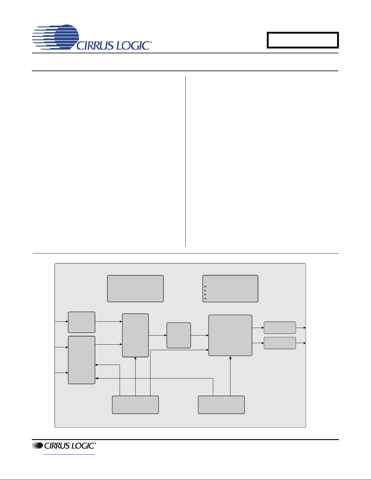
CS8416
S/PDIF
Receiver
(Optional separate VL)
PCM Clocks/Data
PCM Clocks/Data
CS8416 serial port
format
CS8416 Reset
Hardware Control
+3.3V Power
PCM Mux
and Level
Shifter
PCM source select
Switches
Indicator LEDs
S/PDIF Error
S/PDIF or PCM Input Selected
+3.3V power
VL power
External
System
Connector
CS4353 Settings
Copyright © Cirrus Logic, Inc. 2008
(All Rights Reserved)
PCM Clocks/DataPCM Clocks/Data
CS4353
Reset Circuit
AOUTA
Analog Outputs
AOUTB
CS4353 Reset
AUG '08
DS803DB2
Page 2

TABLE OF CONTENTS
1. CDB4353 SYSTEM OVERVIEW ............................................................................................................ 4
2. CS4353 DIGITAL-TO-ANALOG CONVERTER ..................................................................................... 4
3. CS8416 DIGITAL AUDIO RECEIVER .................................................................................................... 4
4. INPUT FOR CLOCKS AND DATA ......................................................................................................... 4
5. POWER SUPPLY CIRCUITRY ............................................................................................................... 5
6. GROUNDING AND POWER SUPPLY DECOUPLING .......................................................................... 5
7. HARDWARE CONTROL ........................................................................................................................ 5
8. CS8416 AND CS4353 RESET ............. ... ... ... .... ... ... ... .... ... ... ... .... ... ... ... ... .... ........................................... 5
9. ANALOG OUTPUT FILTERING .............................. ... .... ... ... ... .... ... ... ... ... ............................................... 5
10. BOARD CONNECTIONS AND SETTINGS .......................................................................................... 6
11. PERFORMANCE PLOTS ..................................................................................................................... 7
12. SCHEMATICS AND LAYOUT ....................................................................................................... 12
13. REVISION HISTORY .........................................................................................................................18
LIST OF FIGURES
Figure 1. FFT (48 kHz, 0 dB) .................... ... ... ... .... ... ... ... .... ... ... ... .... ...........................................................7
Figure 2. FFT (48 kHz, -60 dB) ................................................. ... .... ... ... ... ... .... ... ... ... .... ... ... ........................ 7
Figure 3. FFT (48 kHz, No Input) ................................................................................................................7
Figure 4. FFT (48 kHz Out-of-Band, No Input) ................................. ........................................................... 7
Figure 5. 48 kHz, THD+N vs. Input Freq .....................................................................................................7
Figure 6. 48 kHz, THD+N vs. Level ............................................................................................................ 7
Figure 7. 48 kHz, Fade-to-Noise Linearity .................................................................................................. 8
Figure 8. 48 kHz, Frequency Response ...................................................................................................... 8
Figure 9. 48 kHz, Crosstalk ......................................................................................................................... 8
Figure 10. 48 kHz, Impulse Response ......................... ............................................................................... 8
Figure 11. FFT (96 kHz, 0 dB) .................................................................................................................... 8
Figure 12. FFT (96 kHz, -60 dB) ................................................................................................................. 8
Figure 13. FFT (96 kHz, No Input) .............................................................................................................. 9
Figure 14. FFT (96 kHz Out-of-Band, No Input) ..........................................................................................9
Figure 15. 96 kHz, THD+N vs. Input Freq .............. ... ....................................................... ... ... ... .... ..............9
Figure 16. 96 kHz, THD+N vs. Level . .... ... ... ... ....................................................... ... .... ... ... ... ... .................. 9
Figure 17. 96 kHz, Fade-to-Noise Linearity ................................................................................................ 9
Figure 18. 96 kHz, Frequency Response ..................................... .......... .......... ......... .......... .......... .............. 9
Figure 19. 96 kHz, Crosstalk ..................................................................................................................... 10
Figure 20. 96 kHz, Impulse Response ......................... ............................................................................. 10
Figure 21. FFT (192 kHz, 0 dB) ................................................................................................................ 10
Figure 22. FFT (192 kHz, -60 dB) ............................................................................................................. 10
Figure 23. FFT (192 kHz, No Input) .......................................................................................................... 10
Figure 24. FFT (192 kHz Out-of-Band, No Input) ................................................................................
Figure 25. 192 kHz, THD+N vs. Input Freq ............................................................................................... 11
Figure 26. 192 kHz, THD+N vs. Level ......................................................................................................11
Figure 27. 192 kHz, Fade-to-Noise Linearity ............................................................................................ 11
Figure 28. 192 kHz, Frequency Response ................................................................................................ 11
Figure 29. 192 kHz, Crosstalk ................................................... ... .... ... ... ... ................................................ 11
Figure 30. 192 kHz, Impulse Response .................... ... ... .... ... ... ... .......................................................... ... 11
Figure 31. System Block Diagram and Signal Flow .................................................................................. 12
Figure 32. CS8416 and CS4353 ........................ .... ... ... ... .... ... ... ... .... ... ... ... ... .... ... ... ... .... ... ... ... ... ................13
Figure 33. HW Configuration, PCM Header, and Power ........................................................................... 14
Figure 34. Silkscreen Top ......................................................................................................................... 15
Figure 35. Top Side ................................................................................................................................... 16
Figure 36. Bottom Side ................ ... ... .... ... ... ... ....................................................... ... ................................ 17
CDB4353
...... 10
2 DS803DB2
Page 3

LIST OF TABLES
Table 1. Switch S1 Quick Setup .................................................................................................................. 5
Table 2. System Connections .................................................................................................................... 6
Table 3. CDB4353 Jumper Settings ............................................................................................................ 6
Table 4. CDB4353 Switch Settings ............................................................................................................. 6
CDB4353
DS803DB2 3
Page 4

CDB4353
1. CDB4353 SYSTEM OVERVIEW
The CDB4353 evaluation board is an excellent means of quickly evaluating the CS4353. The CS8416 digital audio
interface receiver provides an easy interface to digital audio signal sources, including the majority of digital audio
test equipment. The evaluation board also allo ws the user to supply e xternal PCM clocks and data throug h two separate header options for system development. Configurati on of the CDB4353 can be m odified through p iano switch
S1, see Table 4. The CDB4353 system block diagram and signal flow is shown in Figure 31, and the CDB4353
schematics are shown in Figures 32 and 33.
2. CS4353 DIGITAL-to-ANALOG CONVERTER
A description of the CS4353 is included in the CS4353 datasheet.
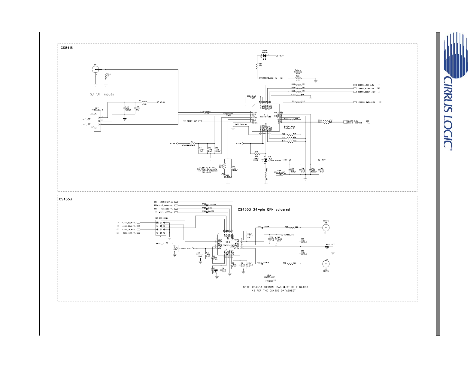
3. CS8416 DIGITAL AUDIO RECEIVER
The system receives and decodes the standard S/PDIF data format using a CS8416 Digital Audio Receiver,
Figure 32. The outputs of the CS8416 include a serial bit clock, serial data, left-ri ght clock, and a 128/256 Fs master
clock. The operation of the CS8416 and a discussion of the digital audio interface is included in the CS8416
datasheet.
The evaluation board has been designed such that the input can be either optical or coaxial, see Figure 32. However, both inputs cannot be driven simultaneously.
Position 3 of piano switch S1 sets the CS8416 output data format to either I²S (down) or LJ (up). Position 2 of S1
sets the output MCLK to LRCK ratio of the CS8416. This switch should be set to 256 (down) for input F s<=48 kHz
and can be either 256 (down) or 128 (up) for Fs>48 kHz. The CS8416 must be manually reset via S2 after either
switch has been toggled for the change to take effect.
4. INPUT FOR CLOCKS AND DATA
The evaluation board has been designed to allow interfacing to external systems via headers J13 and J4. H eader
J13 allows the evaluation board to accept externally generated PCM clocks and da ta at a nomina l voltage of 3.3 V.
The PCM clocks and data are buffered, level-shifted to the VL supply, and then inp ut to the CS4353. The schematic
for the clock/data input is shown in Figure 33. Position 1 of S1 selects the CS4353 PCM source as either the CS8416
(up) or header J13 (down).
Note: If the VL supply is set to a low voltage level (VL<1.8 V), termination resistors may need to be ad ded to the
J13 header signals to match the source and transmission-line impedances that are driving the header. This
may be accomplished by soldering resistors across the rows of J13 on the back of the evaluation board.
Header J4 bypasses position 1 of S1 and allow s for a direct connection of PCM clocks and data to the CS4353.
Under normal operation, shunts placed across the left two rows of J4 connects the PCM clocks and data from the
source specified by position 1 of S1 to the CS4353. An external system can be directly conn ected to the CS4353 by
removing the shunts on J4 and connecting PCM clocks and data across the right two rows of J4 using a ribbon cable.
A single row of “GND” pins are provided to maintain signal ground integrity. Signals input to header J4 must be at
the same voltage level as the VL supply on the evaluation board. The schematic for the header J4 and CS4353 is
shown in Figure 32.
Please see the CS4353 datasheet for more information on clocking data into the CS4353.
4 DS803DB2
Page 5
CDB4353
5. POWER SUPPLY CIRCUITRY
Power is supplied to the evaluation board by two binding posts, GND and +3.3 V (see Figure 33). The allowable
input voltage range for the binding posts is 3.13 V to 3.47 V. The VL supply can be connected to the +3.3 V binding
post by shunting J1 or provided externally by removing the shunt on J1 and connecting another voltage to pin 2 of
J1 (labeled VL). VCP and VA are normally supplied by the 3.3 V binding post but can be set to separate voltages
by removing the shunts on J8 and J10, removing R9 and R14, and then applying external voltages to pin 1 of J8
and J10.
Power consumption of the CS4353 can be measured through the voltage drop at J8, J9, and J10 when the shunts
are removed.
WARNING:Refer to the CS4353 datasheet for maximum allowable voltages levels. Operatio n outside of this range
can cause permanent damage to the device.
6. GROUNDING AND POWER SUPPLY DECOUPLING
As with any high-performance converter, the CS4353 requires careful attention to power supply and grounding arrangements to optimize performance. Figure 32 details the connections to the CS4353 and Figures 34, 35, and 36
show the component placement and top and bottom layout. The decoupling capacitors are located as close to the
CS4353 as possible.
7. HARDWARE CONTROL
The CDB4353 is controlled through settings on switch S1. This allows for configuration of the board without a PC.
Switch S1 can toggle settings for CS8416 MCLK speed, CS8416 and CS4353 PCM data format, clock and data
source for the board, and the Hardware Mode configuration of the CS4353. Table 1 below shows S1 settings for
S/PDIF input and PCM input header quick setup modes. See Table 4 for details on each switch S1 setting.
S1 POSITION S/PDIF INPUT - OPT1 or J16 PCM INPUT - J3
1Up Down
2 Down Down
3 Down Down
4Up Up
5 Down Down
Table 1. Switch S1 Quick Setup
8. CS8416 AND CS4353 RESET
Pressing switch S2 resets the CS8416. Jumper J5 sets whether the CS4353 is reset by switch S2 (External) or by
the CS4353’s internal power-on reset function (POR).
9. ANALOG OUTPUT FILTERING
The analog output on the CDB4353 has been designed according to th e CS4353 datasheet. This output circuit consists of a single-pole R and C filter. J11 selects the output ground reference for the CS4353. The output reference
can be set to the evaluation board’s ground (shunted) or J14 and J15’s ground connection (not shunted). See
Figure 33 for details of CS4353 output filter.
DS803DB2 5
Page 6
10.BOARD CONNECTIONS AND SETTINGS
Board connections and settings are shown in Table 2, Table 3, and Table 4 below.
CONNECTOR INPUT/OUTPUT SIGNAL PRESENT
3.3 V - J3 Input +3.3 V power for the evaluation board
GND - J2 Input Ground connection from power supply
SPDIF INPUT - J16 Input Digi tal audio interfac e input via coaxial cable
SPDIF INPUT - OPT1 Input Digital audio interface input via optical cable
PCM INPUT - J13 Input In put for master, serial, left/right clocks and serial data
EXT SYS CONN - J4 Input
AOUTA - J14
AOUTB - J15
Output
JUMPER PURPOSE POSITION FUNCTION SELECTED
J1
J8 Current measure for VCP *shunted
J9 Current measure for VL *shunted
J10 Current measure for VA *shunted
J5 CS4353 Reset Select
J1 1 CS4353 Output Reference
Selects source of voltage for
the VL supply
Input for master, serial, left/right clocks and serial data - direct to CS4353
RCA line-level analog outputs
Table 2. System Connections
*shunted
not shunted
*EXTERNAL
POR
*shunted
not shunted
Voltage source is +3.3 V binding post (J3)
Voltage source is pin 2 of J1
When shunt is removed, the voltage can be measured
across a fixed resistance to determine current.
When shunt is removed, the voltage can be measured
across a fixed resistance to determine current.
When shunt is removed, the voltage can be measured
across a fixed resistance to determine current.
CS4353 reset by S2
CS4353 uses internal power-on reset
Output reference is board ground
Output reference is J14 and J15 ground
CDB4353
Table 3. CDB4353 Jumper Settings
SWITCH PURPOSE POSITION FUNCTION SELECTED
Selects PCM source for
CS4353
CS8416 MCLK/LRCK Ratio 2
S1
S2 Resets CS4353 and CS8416 -
CS8416 and CS4353 PCM
Format
CS4353 Output Amplitude 4
CS4353 De-emphasis select 5
Table 4. CDB4353 Switch Settings
1
3
CS8416 must be reset if switch S1 position 2 or 3 is
down = PCM Header J3
*up = CS8416
*down = MCLK is 256xFs
up = MCLK is 128xFs
2
rms
rms
S
output
output
*down = I
up = LJ
down = 1 V
*up = 2 V
*down = De-emphasis off
up = De-emphasis on
changed
Note: All settings denoted by an asterisk (*) are the Default Factory Settings.
6 DS803DB2
Page 7

CDB4353
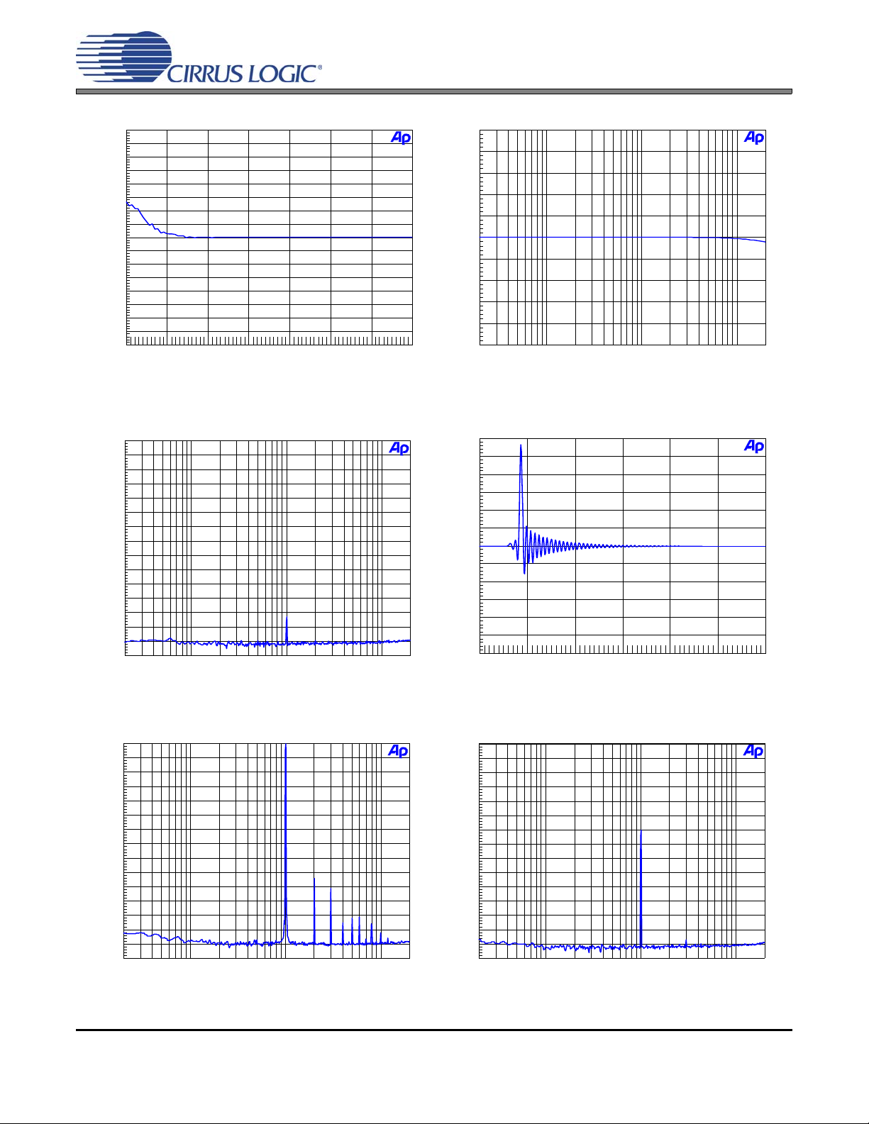
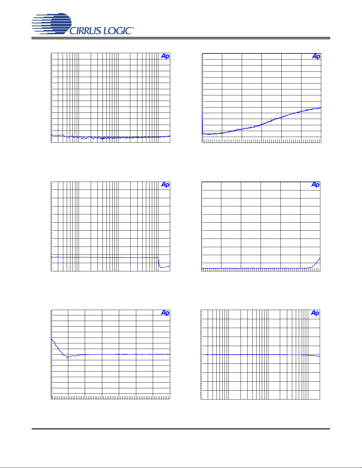
11.PERFORMANCE PLOTS
Test conditions (unless otherwise specified): TA = 25°C; VCP = VA = VL = 3.3 V; AGND = DGND =CPGND = 0 V;
OPT1 S/PDIF input source; PCM data Left-Justified format; 2 V
997 Hz sine wave at 0 dBFS; dB values relative to 2.1 V
RMS
20 kHz. CDB4353 revision A3 with CS4353 revision B1 used.
+0
-10
-20
-30
-40
-50
-60
d
-70
B
r
-80
A
-90
-100
-110
-120
-130
-140
-150
20 20k50 100 200 500 1k 2k 5k 10k
Hz
d
B
r
A
Figure 1. FFT (48 kHz, 0 dB) Figure 2. FFT (48 kHz, -60 dB)
+0
-10
-20
-30
-40
-50
-60
d
-70
B
r
-80
A
-90
-100
-110
-120
-130
-140
-150
20 20k50 100 200 500 1k 2k 5k 10k
Hz
d
B
r
A
Figure 3. FFT (48 kHz, No Input) Figure 4. FFT (48 kHz Out-of-Band, No Input)
+0
-10
-20
-30
-40
d
-50
B
r
-60
A
-70
-80
-90
-100
-110
20 20k50 100 200 500 1k 2k 5k 10k
Hz
d
B
r
A
Figure 5. 48 kHz, THD+N vs. Input Freq Figure 6. 48 kHz, THD+N vs. Level
output; De-emphasis off; input test signal is a
RMS
full-scale output; measurement bandwidth 10 Hz to
+0
-10
-20
-30
-40
-50
-60
-70
-80
-90
-100
-110
-120
-130
-140
-150
20 20k50 100 200 500 1k 2k 5k 10k
+0
-10
-20
-30
-40
-50
-60
-70
-80
-90
-100
-110
-120
-130
-140
-150
+0
-10
-20
-30
-40
-50
-60
-70
-80
-90
-100
-110
-120 +0-100 -80 -60 -40 -20
20k 120k40k 60k 80k 100k
Hz
Hz
dBFS
DS803DB2 7
Page 8
CDB4353
+40
+35
+30
+25
+20
+15
+10
d
+5
B
+0
r
-5
A
-10
-15
-20
-25
-30
-35
-40
-140 +0-120 -100 -80 -60 -40 -20
dBFS
+5
+4
+3
+2
+1
d
B
+0
r
A
-1
-2
-3
-4
-5
20 20k50 100 200 500 1k 2k 5k 10k
Hz
Figure 7. 48 kHz, Fade-to-Noise Linearity Figure 8. 48 kHz, Frequency Response
+0
-10
-20
-30
-40
-50
-60
d
-70
B
r
-80
A
-90
-100
-110
-120
-130
-140
-150
20 20k50 100 200 500 1k 2k 5k 10k
Hz
3
2.5
2
1.5
1
500m
0
V
-500m
-1
-1.5
-2
-2.5
-3
0 3m500u 1m 1.5m 2m 2.5m
sec
Figure 9. 48 kHz, Crosstalk Figure 10. 48 kHz, Impulse Response
+0
-10
-20
-30
-40
-50
-60
d
-70
B
r
-80
A
-90
-100
-110
-120
-130
-140
-150
20 20k50 100 200 500 1k 2k 5k 10k
Hz
+0
-10
-20
-30
-40
-50
-60
d
B
-70
r
-80
A
-90
-100
-110
-120
-130
-140
-150
20 20k50 100 200 500 1k 2k 5k 10k
Hz
Figure 11. FFT (96 kHz, 0 dB) Figure 12. FFT (96 kHz, -60 dB)
8 DS803DB2
Page 9
CDB4353
+0
-10
-20
-30
-40
-50
-60
d
-70
B
r
-80
A
-90
-100
-110
-120
-130
-140
-150
20 20k50 100 200 500 1k 2k 5k 10k
Hz
Figure 13. FFT (96 kHz, No Input) Figure 14. FFT (96 kHz Out-of-Band, No Input)
+0
-10
-20
-30
-40
d
-50
B
r
-60
A
-70
-80
-90
-100
-110
20 20k50 100 200 500 1k 2k 5k 10k
Hz
+0
-10
-20
-30
-40
-50
-60
d
B
-70
r
-80
A
-90
-100
-110
-120
-130
-140
-150
+0
-10
-20
-30
-40
d
-50
B
r
-60
A
-70
-80
-90
-100
-110
-120 +0-100 -80 -60 -40 -20
20k 120k40k 60k 80k 100k
Hz
dBFS
Figure 15. 96 kHz, THD+N vs. Input Freq Figure 16. 96 kHz, THD+N vs. Level
+40
+35
+30
+25
+20
+15
+10
d
+5
B
+0
r
-5
A
-10
-15
-20
-25
-30
-35
-40
-140 +0-120 -100 -80 -60 -40 -20
dBFS
+5
+4
+3
+2
+1
d
B
+0
r
A
-1
-2
-3
-4
-5
20 20k50 100 200 500 1k 2k 5k 10k
Hz
Figure 17. 96 kHz, Fade-to-Noise Linearity Figure 18. 96 kHz, Frequency Response
DS803DB2 9
Page 10

CDB4353
+0
-10
-20
-30
-40
-50
-60
d
-70
B
r
-80
A
-90
-100
-110
-120
-130
-140
-150
20 20k50 100 200 500 1k 2k 5k 10k
Hz
Figure 19. 96 kHz, Crosstalk Figure 20. 96 kHz, Impulse Response
+0
-10
-20
-30
-40
-50
-60
d
-70
B
r
-80
A
-90
-100
-110
-120
-130
-140
-150
20 20k50 100 200 500 1k 2k 5k 10k
Hz
3
2.5
2
1.5
1
500m
0
V
-500m
-1
-1.5
-2
-2.5
-3
0 1.5m500u 1m
+0
-10
-20
-30
-40
-50
-60
d
B
-70
r
-80
A
-90
-100
-110
-120
-130
-140
-150
20 20k50 100 200 500 1k 2k 5k 10k
sec
Hz
Figure 21. FFT (192 kHz, 0 dB) Figure 22. FFT (192 kHz, -60 dB)
+0
-10
-20
-30
-40
-50
-60
d
-70
B
r
-80
A
-90
-100
-110
-120
-130
-140
-150
20 20k50 100 200 500 1k 2k 5k 10k
Hz
+0
-10
-20
-30
-40
-50
-60
d
B
-70
r
-80
A
-90
-100
-110
-120
-130
-140
-150
20k 120k40k 60k 80k 100k
Hz
Figure 23. FFT (192 kHz, No Input) Figure 24. FFT (192 kHz Out-of-Band, No Input)
10 DS803DB2
Page 11

CDB4353
+0
-10
-20
-30
-40
d
-50
B
r
-60
A
-70
-80
-90
-100
-110
20 20k50 100 200 500 1k 2k 5k 10k
Hz
+0
-10
-20
-30
-40
d
-50
B
r
-60
A
-70
-80
-90
-100
-110
-120 +0-100 -80 -60 -40 -20
dBFS
Figure 25. 192 kHz, THD+N vs. Input Freq Figure 26. 192 kHz, THD+N vs. Level
+40
+35
+30
+25
+20
+15
+10
d
+5
B
+0
r
-5
A
-10
-15
-20
-25
-30
-35
-40
-140 +0-120 -100 -80 -60 -40 -20
dBFS
+5
+4
+3
+2
+1
d
B
+0
r
A
-1
-2
-3
-4
-5
20 20k50 100 200 500 1k 2k 5k 10k
Hz
Figure 27. 192 kHz, Fade-to-Noise Linearity Figure 28. 192 kHz, Frequency Response
+0
-10
-20
-30
-40
-50
-60
d
-70
B
r
-80
A
-90
-100
-110
-120
-130
-140
-150
20 20k50 100 200 500 1k 2k 5k 10k
Hz
3
2.5
2
1.5
1
500m
0
V
-500m
-1
-1.5
-2
-2.5
-3
0 600u200u 400u
sec
Figure 29. 192 kHz, Crosstalk Figure 30. 192 kHz, Impulse Response
DS803DB2 11
Page 12

12 DS803DB2
12.SCHEMATICS AND LAYOUT
PCM Input
Optical
S/PDIF
Input
Coaxial
S/PDIF
Input
PCM HEADER
Figure 33
CS8416
S/PDIF
Receiver
Figure 32
PCM Clocks/Data
PCM Clocks/Data
CS8416 serial port
format
CS8416 Reset
+3.3V Power
(Optional separate VL)
Figure 33
PCM Mux
and Level
Shifter
Figure 33
PCM source select
Hardware Control
Switches
Figure 33
External
System
Connector
Figure 32
CS4353 Settings
Indicator LEDs
S/PDIF Error
S/PDIF or PCM Input Selected
+3.3V power
VL power
PCM Clocks/DataPCM Clocks/Data
CS4353
Figure 32
Reset Circuit
Figure 33
AOUTA
Figure 32
Analog Outputs
AOUTB
Figure 32
CS4353 Reset
Figure 31. System Block Diagram and Signal Flow
CDB4353
Page 13
DS803DB2 13
Figure 32. CS8416 and CS4353
CDB4353
Page 14
14 DS803DB2
Figure 33. HW Configuration, PCM Header, and Power
CDB4353
Page 15

DS803DB2 15
Figure 34. Silkscreen Top
CDB4353
Page 16

16 DS803DB2
Figure 35. Top Side
CDB4353
Page 17

DS803DB2 17
Figure 36. Bottom Side
CDB4353
Page 18

13.REVISION HISTORY
Release Changes
DB1 Initial Release
DB2 Updated block diagram on page 1 and Figure 31.
Updated features and description on page 1.
Updated plots in Section 11. Performance Plots.
Updated Figure 32 and Figure 33.
CDB4353
Contacting Cirrus Logic Support
For all product questions and inquiries, contact a Cirrus Logic Sales Representative.
To find the one nearest you, go to www.cirrus.com.
IMPORTANT NOTICE
Cirrus Logic, Inc. and its subsidiaries ("Cirrus") believe that the information contained in this document is accurate and reliable. However, the information is subject
to change without not ice and is pr ovided "AS IS" witho ut warr anty of any kind (express or implied). Customers are advised to obtain the latest version of relevant
information to verify, before placing orders, that information being relied on is current and complete. All products are sold subject to the terms and conditions o f sale
supplied at the time of order acknowledgment, including those pertaining to warranty, indemnification, and limitation of liability. No responsibility is assumed by Cirrus
for the use of this information, including use of this information as the basis for manufacture or sale of any items, or for infringement of patents or other rights of third
parties. This document is the property of Cirrus and by furnishing this information, Cirrus grants no license, express or implied under any patents, mask work rights,
copyrights, trademarks, trade secrets or other inte llectual property rig hts. Cirrus owns the copyrights associated with the information contained herein and gives consent for copies to be made of the information only for use within your organization with respect to Cirrus integrated circuits or other products of Cirrus. This consent
does not extend to other copying such as copying for general distribution, advertising or promotional purposes, or for creating any work for resale.
CERTAIN APPLICATIONS USING SEMICONDUCTOR PRODUCTS MAY INVOLVE POTENTIAL RISKS OF DEATH, PERSONAL INJURY, OR SEVERE PROPERTY OR ENVIRONMENTAL DAMAGE (“CRITICAL APPLICATIONS”). CIRRUS PRODUCTS ARE NOT DESIGNED, AUTHORIZED OR WARR ANTED FOR USE
IN PRODUCTS SURGICALLY IMPLANTED INTO THE BODY, AUTOMOTIVE SAFETY OR SECURITY DEVICES, LIFE SUPPORT PRODUCTS OR OTHER CRITICAL APPLICATIONS. INCLUSION OF CIRRUS PRODUCTS IN SUCH APPLICATIONS IS UNDERSTOOD TO BE FULLY AT THE CUSTOM ER’S RISK AND CIRRUS DISCLAIMS AND MAKES NO WARRANTY, EXPRESS, STATUTORY OR IMPLIED, INCLUDING THE IMPLIED WARR ANTIES OF MERCHANTABILITY AND
FITNESS FOR PARTICULAR PURPOSE, WITH REGARD TO ANY CIRRUS PRODUCT THAT IS USED IN SUCH A MANNER. IF THE CUSTOMER OR CUSTOMER’S CUSTOMER USES OR PERMITS THE USE OF CIRRUS PRODUCTS IN CRITICAL APPLICATIONS, CUSTOMER AGREES, BY SUCH USE, TO FULLY
INDEMNIFY CIRRUS, ITS OFFICERS, DIRECTORS, EMPLOYEES, DISTRIBUTORS AND OT HER AGE NTS FRO M ANY AND AL L LI ABI L IT Y, I NCL UDING ATTORNEYS’ FEES AND COSTS, THAT MAY RESULT FROM OR ARISE IN CONNECTION WITH THESE USES.
Cirrus Logic, Cirrus, and the Cirrus Logic logo design s ar e tra de m a rks of Ci rru s Lo gi c, Inc. All o ther bra nd and product names in this document may be trademarks
or service marks of their respective owners.
18 DS803DB2
 Loading...