

Page 1
Evaluation Board for CS4351
CDB4351
Features
Demonstrates recommended layout and
grounding arrangements.
CS8416 receives S/PDIF, & EIAJ-340compatible digital audio.
Headers for Ext ernal PCM Aud io and Control
Input
Requires only a digital signal source and
power supplies for a complete Digital-toAnalog Converter system.
Description
The CDB4351 evalua tion board is an excellent means
for quickly evaluating the CS4351 24-bit, high performance stereo D/A converter. Evaluation requires an
analog signal analyzer, a digital signal source, a P C for
controlling the CS4351 (stand alone operation is also
available) and a power supply. Analog line-level outputs
are provided via RCA phono jacks.
The CS8416 digital audio receiver IC. provides the system timing necessary to operate the Digital-to-Analog
converter and will accept S/PDIF, and EIAJ-340-compatible audio data. The evaluation board may also be
configured to accept external timing and data signals for
operation in a user application during system
development.
ORDERING INFORMATION
CDB4351 Evaluation Board
Inputs for Clocks
and Data
CS8416
Digital Au d io
In terfac e
http://www.cirrus.com
Control
Port
CS43 51
Copyright © Cirrus Logic, Inc. 2004
(All Rights Reserved)
Analog Outputs
and Mu ting
OCT ‘04
DS566DB3
1
Page 2

TABLE OF CONTENTS
1. CS4351 DIGITAL TO ANALOG CONVERTER . . . . . . . . . . . . . . . . . . . . . . . . . . . . . . . . . . . .3
2. CS8416 DIGITAL AUDIO RECEIVER . . . . . . . . . . . . . . . . . . . . . . . . . . . . . . . . . . . . . . . . . . .3
3. INPUT FOR CLOCKS AND DATA . . . . . . . . . . . . . . . . . . . . . . . . . . . . . . . . . . . . . . . . . . . . . .3
4. POWER SUPPLY CIRCUITRY . . . . . . . . . . . . . . . . . . . . . . . . . . . . . . . . . . . . . . . . . . . . . . . . .3
5. GROUNDING AND POWER SUPPLY DECOUPLING . . . . . . . . . . . . . . . . . . . . . . . . . . . . . .4
6. CONTROL PORT SOFTWARE . . . . . . . . . . . . . . . . . . . . . . . . . . . . . . . . . . . . . . . . . . . . . . . .4
7. ANALOG OUTPUT FILTERING . . . . . . . . . . . . . . . . . . . . . . . . . . . . . . . . . . . . . . . . . . . . . . . .4
8. DESIGN NOTE . . . . . . . . . . . . . . . . . . . . . . . . . . . . . . . . . . . . . . . . . . . . . . . . . . . . . . . . . . . . .5
LIST OF FIGURES
Figure 1. System Block Diagram and Signal Flow. . . . . . . . . . . . . . . . . . . . . . . . . . . . . . . . . . .6
CDB4351
Figure 2. CS4351 . . . . . . . . . . . . . . . . . . . . . . . . . . . . . . . . . . . . . . . . . . . . . . . . . . . . . . . . . . . . . .7
Figure 3. Analog Outputs . . . . . . . . . . . . . . . . . . . . . . . . . . . . . . . . . . . . . . . . . . . . . . . . . . . . . . . 8
Figure 4. PCM Input Headers . . . . . . . . . . . . . . . . . . . . . . . . . . . . . . . . . . . . . . . . . . . . . . . . . . . . 9
Figure 5. CS8416 S/PDIF Input. . . . . . . . . . . . . . . . . . . . . . . . . . . . . . . . . . . . . . . . . . . . . . . . . .10
Figure 6. Control Port Interface . . . . . . . . . . . . . . . . . . . . . . . . . . . . . . . . . . . . . . . . . . . . . . . . .11
Figure 7. Power Supply Connections . . . . . . . . . . . . . . . . . . . . . . . . . . . . . . . . . . . . . . . . . . . .12
Figure 8. Silkscreen Top. . . . . . . . . . . . . . . . . . . . . . . . . . . . . . . . . . . . . . . . . . . . . . . . . . . . . . .13
Figure 9. Top Side. . . . . . . . . . . . . . . . . . . . . . . . . . . . . . . . . . . . . . . . . . . . . . . . . . . . . . . . . . . . 14
Figure 10. Bottom Side. . . . . . . . . . . . . . . . . . . . . . . . . . . . . . . . . . . . . . . . . . . . . . . . . . . . . . . .15
2 DS566DB3
Page 3

CDB4351
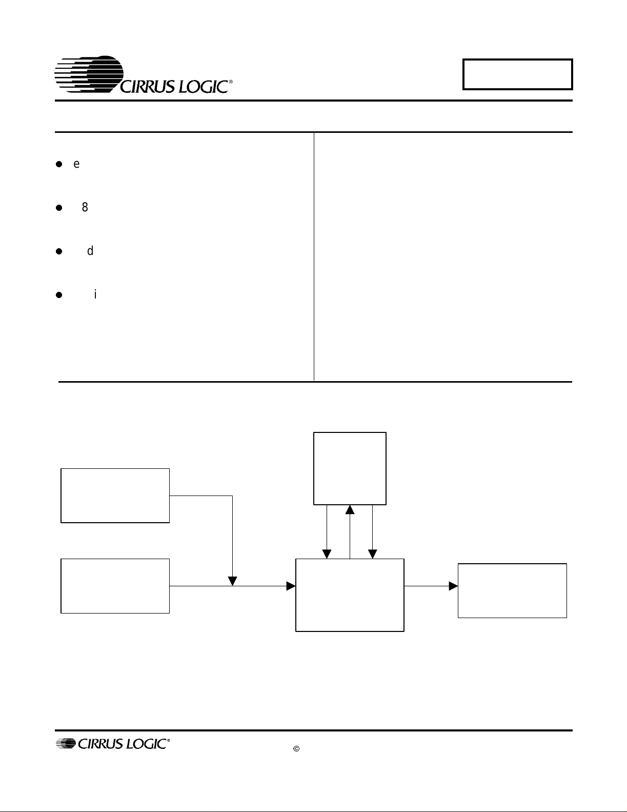
CDB4351 SYSTEM OVERVIEW
The CDB4351 evaluation board is an excellent means of quickly evaluating the CS4351. The
CS8416 digital audio i nterface receiver provide s an easy interface to digita l audio signal sou rces
including the majority of digital audio test equipment. The evaluation board also allows the user
to supply external PCM clocks and data through a header for system development.
The CDB4351 schematic has been partitioned into 6 schematics shown in Figures 2 through 7.
Each partitioned schematic is represented in the system diagram shown in Figure 1. Notice that
the system diagram also includes the interconnections between the partitioned schematics.
1. CS4351 DIGITAL-to-ANALOG CONVERTER
A description of the CS4351 is included in the CS4351 datasheet.
2. CS8416 DIGITAL AUDIO RECEIVER
The system receives and decodes the standard S/PDIF data format using a CS8416 Digital Audio Receiver, F igure 5. The outputs of the CS8416 includ e a serial bit clock, serial data, l eft-ri ght
clock, and a 128/256 Fs master clock. The CS8416 data format is selected by switch S1. The
operation of th e CS8416 an d a discussion of the digital au dio inter face is includ ed in the CS8 416
datasheet.
The evaluat ion b oard has bee n de si gned such that the i npu t can be eithe r optical or coaxial , see
Figure 5. However, both inputs cannot be driven simultaneously.
Positions 1 and 2 of S1 set th e seri al f orma t for t he C S8416. These should match t he setti n gs of
the CS4351 (default is both set to I2S). Position 3 of S1 sets the output MCLK to LRCK ratio of
the CS8416. This switch should be set to 256 (LO) for input Fs<=48 kHz and can be either 256
(LO) or 128 (HI) for Fs>48 kHz
3. INPUT FOR CLOCKS AND DATA
The evaluation board has been designed to allow interfacing to external systems via the header
J9. Header J9 allows the evaluation bo ard to accept exte rnally gen erat ed P CM clocks and d ata.
The schematic for the clock/data input is shown in Figure 4. Switch position 4 of S1 selects the
source as either CS8416 or header J9.
Please see the CS4351 datasheet for more information.
4. POWER SUPPLY CIRCUITRY
Power is supplied to the evaluation board by six binding posts (GND, +5 V, VL, VD, VA, and
VA_H), see Figure 7. The VD, VL, and VA supplies can be jumpered to a +3.3 V regulator and
the +5 V binding post can be jumpered to a 5 V regulator thus requir ing only V A_H an d GND for
ease of use. VD, VL, VA and VA_H should be set to the recommended values stated in the
CS4351 datasheet.
WARNING: Refer to the CS4351 datasheet for maximum allowable voltages levels. Operation
outside of this range can cause permanent damage to the device.
DS566DB3 3
Page 4
CDB4351
5. GROUNDING AND POWER SUPPLY DECOUPLING
As with any high-performance converter, the CS4351 requires careful attention to power supply
and grounding arrangements to optimize performance. Figure 2 details the connections to the
CS4351 and Figures 8, 9, and 10 show the component placement and top and bottom layout.
The decoupling capacitors are located as close to the CS4351 as possible. Extensive use of
ground plane fill in the evaluation board yields large reductions in radiated noise.
6. CONTROL PORT SOFTWARE
The CDB4351 is shipped with Windows 95/98/ME-based software as well as Windows
NT/2000/XP drivers for interfacing with the CS4351 control port via the DB25 connector, J16.
The software can be u sed to comm unicate with the CS435 1 i n e ither SPI® or I2C mode. See the
readme.txt file for more information.
7. ANALOG OUTPUT FILTERING
The analog outp ut on the CDB4351 has be en designed according to th e CS4351 datasheet . This
output circuit includes an AC coupling cap, the FET mute circuit, and a single-pole R and C. An
additional load re sistance of 5.1 k Ω can be jumpered in (J15 and J24) to test the CS4351’ s load
driving capability. The FET muting circuit may be bypassed by placing a shunt on J13 and J21.
CONNECTOR INPUT/OUTPUT SIGNAL PRESENT
+5V Input + 5 V power
VD Input + 3.3 V power for the CS4351 digital supply
VL I nput + 1.8 V to +3.3 V power for the CS4351 serial interface
VA Input + 3.3 V power for the CS4351 low-voltage analog
VA_H Input +9 V to +12 V positive supply for the CS4351 high-voltage analog
GND Input Ground connection from power supply
SPDIF INPUT - J11 Input Digital audio interface input via coaxial cable
SPDIF INPUT - OPT1 Input Digital audio interface input via optical cable
PCM INPUT - J9 Input Input for master, serial, left/right clocks and serial data
PC Port Input/Output
EXT CTRL I/O Input/Output
AOUTA and AOUTB Output RCA line-level analog outputs
Table 1. System Connections
Parallel connection to PC for SPI / I
2
I/O for SPI / I
C control port signals
2
C control port signals
4 DS566DB3
Page 5
CDB4351
JUMPER /
SWITCH PURPOSE POSITION S/C FUNCTION SELECTED
J5 Selects source of voltage
for the +5V suppli e s
J6 Selects source of voltage
for the VD supplies
J7 Selects source of voltage
for the VL supply
J10 Selects source of voltage
for the VA supply
S1 Sets Mode of CS8416 and
clock source
J20 Stand-alone/Control Port
Select
J17 DEM(AD0/CS) HI
J18 DIF0(SDA/CDIN) *HI
J19 DIF1(SCL/CCLK) *HI
J15
J24
J13
J21
LOAD select SHUNTED
Mute Disable *SHUNTED
+5 V
*+5V_REG
VD
*+3.3V REG
VL
*+3.3V REG
VA
*+3.3V REG
*1 = open
*2, 3, 4 = closed
DIS
*EN
*LO
LO
LO
*OPEN
OPEN
Voltage source is +5 V binding post
Voltage source is VD binding post
Voltage source is +3.3 V regulator
Voltage source is VL binding post
Voltage source is +3.3 V regulator
Voltage source is VA binding post
Voltage source is +3.3 V regulator
Default setting is I
See CS8416 datasheet for details
S
C
-
SC
C
S
C
S
Stand-alone Mode (No PC required)
Control Port Mode (PC required)
See CS4351 datasheet for details
See CS4351 datasheet for details
See CS4351 datasheet for details
Voltage source is +5 V regulator
2
S mode from CS8416
Adds resistor for max loading
Normal output circuit
Bypasses FET muti n g
Normal output circuit
Table 2. CDB4351 Jumper Settings
*Default Factory Settings.
The S/C column denotes standard jumper settings for either stand-alone (S) or control port (C) operation.
8. DESIGN NOTE CDB4351 Revision A.0
The FET muting ci rcuit must be bypassed by pl acing a shunt on J13 and J21, oth erwise unwan ted noise will occur while muted.
CDB4351 Revision B.0
There are no known issues on this revision.
DS566DB3 5
Page 6

CDB4351
Figure 7
Power
Figure 6
Control Port
Channel A
Channel B
Outputs and Mute
Figure 3
Outputs and Mute
CS4351
Figure 3
Figure 2
Reset
Circuit
MCLK
SCLK
LRCK
SDIN
Figure 5
8416 Digital
Audio Receiver
6 DS566DB3
Figure 4
PCM Inputs
Figure 1. System Block Diagram and Signal Flow
Page 7

CDB4351
Figure 2. CS4351
DS566DB3 7
Page 8

CDB4351
Figure 3. Analog Outputs
8 DS566DB3
Page 9

CDB4351
Figure 4. PCM Input Headers
DS566DB3 9
Page 10

CDB4351
Figure 5. CS8416 S/PDIF Input
10 DS566DB3
Page 11

CDB4351
Figure 6. Control Port Interface
DS566DB3 11
Page 12

CDB4351
Figure 7. Power Supply Connections
12 DS566DB3
Page 13
CDB4351
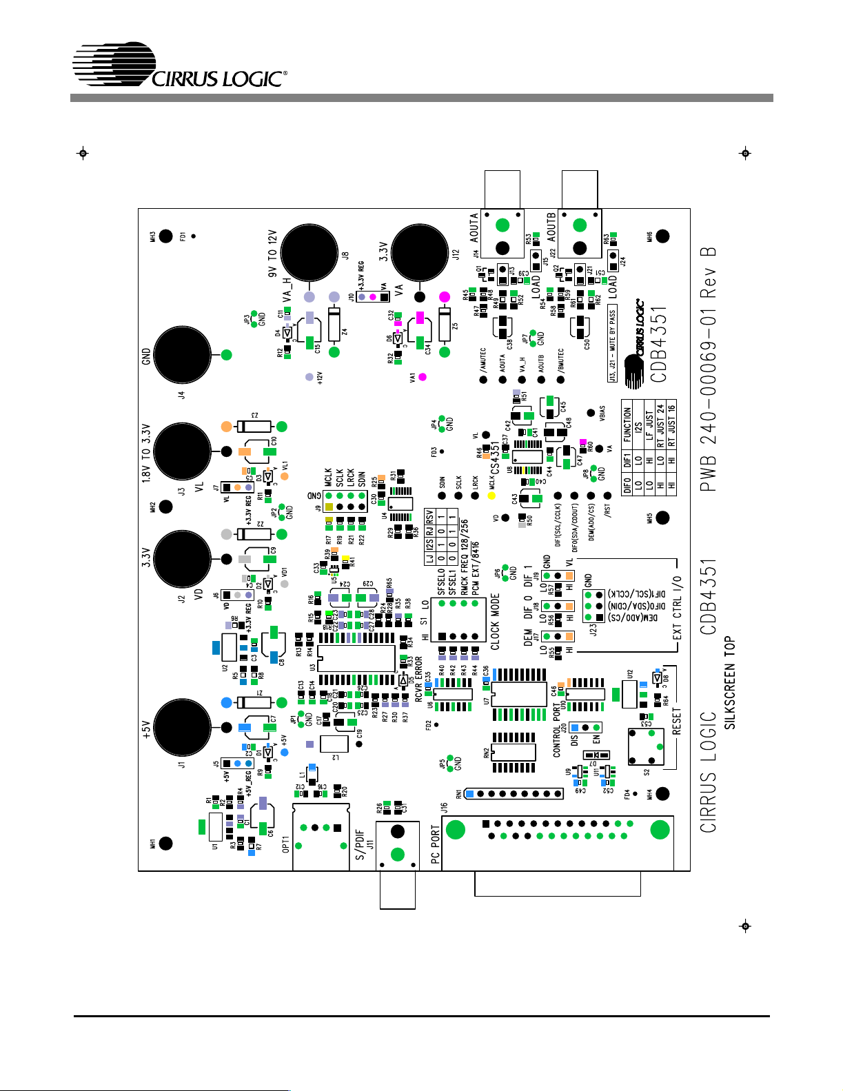
Figure 8. Silkscreen Top
DS566DB3 13
Page 14

CDB4351
Figure 9. Top Si de
14 DS566DB3
Page 15

CDB4351
Figure 10. Bott om S id e
DS566DB3 15
Page 16

REVISION HISTORY
Release Date Changes
DB1 November 2003 Initial Release
DB2 June 2004 Updated figures 2 and 5 (C48 and R65)
DB3 October 2004 Updated schematic and layout figures to match rev B of the PCB
CDB4351
Contacting Cirrus Logic Support
For all product questions and inquiries contact a Cirrus Logic Sales Representative.
To find one nearest you go to www.cirrus.com
IMPORTANT NOTICE
Cirrus Logic, Inc. and its subsidiaries ("Cirrus") believe that the information contained in this document is accurate and reliable. However, the information is sub-
ject to change wit hout notice and is provided "AS IS" wit hout warranty of any kind (express or implied). Customers are advised to obtain the latest version of
relevant information to verify, before placing orders, that information being relied on is current and complete. All products are sold subject to the terms and conditions of sale supplied at the time of order acknowledgment, including those pertaining to warranty, patent infringement, and limitation of liability. No responsibility is assumed by Cirrus for the use of this information, including use of this information as the basis for manufacture or sale of any items, or for infringement
of patents or other rights of third parties. This document is the property of Cirrus and by furnishing this information, Cirrus grants no license, express or implied
under any patents, mask work rights, copyrights, trademarks, trade secrets or other intellectual property rights. Cirrus owns the copyrights associated with the
information contained herein and gives consent for copies to be made of the information only for use within your organization with respect to Cirrus integrated
circuits or other products of Cirrus. This consent does not extend to other copying such as copying for general distribution, advertising or promotional purposes,
or for creating any work for resale.
CERTAIN APPLI CATI ONS USING SEMICO NDUCTOR PRODUCTS MAY INVOLVE POTENTI AL RI SKS OF DEATH, PERSONAL I NJURY, OR SEVERE
PROPERTY OR ENVIRONMENTAL DAMAGE ("CRITICAL APPLICATIONS"). CIRRUS PRODUCTS ARE NOT DESIGNED, AUTHORIZED OR WARRANTED
FOR USE IN AIRCRAFT SYSTEMS, MILITARY APPLICATI O NS, PRODUCTS SURGICALLY IMPLANTED INTO THE BODY, LIFE SUPPORT PRODUCTS
OR OTHER CRITICAL APPLICATIONS (INCLUDING MEDICAL DEVICES, AIRCRAFT SYSTEMS OR COMPONENTS AND PERSONAL OR AUTOMOTIVE
SAFETY OR SECURITY DEVICES). INCLUSION OF CIRRUS PRODUCTS IN SUCH APPLICATIONS IS UNDERSTOOD TO BE FULLY AT THE CUSTOMER'S RISK AND CIRRUS DISCLAIMS AND MAKES NO WARRANTY, EXPRESS, STATUTORY OR IMPLIED, INCLUDING THE IMPLIED WARRANTIES OF
MERCHANTABILITY AND FITNESS FOR PARTICULAR PURPOSE, WITH REGARD TO ANY CIRRUS PRODUCT THAT IS USED IN SUCH A MANNER. IF
THE CUSTOMER OR CUSTOMER'S CUSTOMER USES OR PERMITS THE USE OF CIRRUS PRODUCTS IN CRITICA L APPLICAT IONS, CUSTOMER
AGREES, BY SUCH USE , TO FULLY INDEMNIFY CIRRUS, ITS OFFICE RS, DIRECTORS, E MPLOYE ES, DISTRI BUTORS AND OTHER AGENTS FROM
ANY AND ALL LIABILITY, INCLUDING ATTORNEYS' FEES AND COSTS, THAT MAY RESULT FROM OR ARISE IN CONNECTION WITH THESE USES.
Cirrus Logic, Cirr us, and the Cirrus Logi c logo designs are trademarks of Cirrus Logic, Inc. All other brand and product names in this document may be trad emarks or service marks of their respective owners.
2
C is a regi st er ed tr ademar k of Phi lips Semiconductor . Purcha se of I2C Components of Cir r us Log ic , I nc. , o r one of it s subl ic ens ed Associ ate d Compani es
I
conveys a license under the Philips I
16 DS566DB3
2
C Patent Rights to use those components in a standard I2C system.
 Loading...