

Page 1
Evaluation Board for CS4352
CDB4352
Features
Demonstrates Recommended Layout And
Grounding Arrangements
CS8416 Receives S/PDIF, & EIAJ-340-
Compatible Digital Audio
Headers for External PCM Audio
Requires Only a Digital Signal Source and
Power Supplies for a Complete Digital-toAnalog Converter System
Description
The CDB4352 evaluation board is an excellent means
for quickly evaluating the CS4352 24-bit, high-performance stereo D/A converter. Evaluation requires an
analog signal analyzer, a digital signal source, and a
power supply. Analog line-level outputs are provided via
RCA phono jacks.
The CS8416 digital audio receiver IC provides the system timing necessary to operate the Digital-to-Analog
converter and will accept S/PDIF and EIAJ-340-compatible audio data. The evaluat ion board may also be
configured to accept external timing and data signals for
operation in a user application during system
development.
ORDERING INFORMATION
CDB4352 Evaluation Board
Clocks/Data
Header
S/PDIF Input
(CS8416)
Reset
http://www.cirrus.com
Hardware Switches
Mux
CS4352
Reset
Copyright © Cirrus Logic, Inc. 2006
(All Rights Reserved)
Analog Output
(Line Level)
Muting
SEPTEMBER '06
DS684DB1
Page 2

TABLE OF CONTENTS
1. CDB4352 SYSTEM OVERVIEW ............................................................................................................ 4
2. CS4352 DIGITAL-TO-ANALOG CONVERTER ..................................................................................... 4
3. CS8416 DIGITAL AUDIO RECEIVER .................................................................................................... 4
4. INPUT FOR CLOCKS AND DATA ......................................................................................................... 4
5. POWER SUPPLY CIRCUITRY ............................................................................................................... 4
6. GROUNDING AND POWER SUPPLY DECOUPLING ..........................................................................5
7. HARDWARE CONTROL ........................................................................................................................ 5
8. ANALOG OUTPUT FILTERING .............................. ... .... ... ... ... .... ... ... ..................................................... 5
9. PERFORMANCE PLOTS ....................................................................................................................... 6
10. DESIGN NOTE ................................................................................................................................... 11
11. SCHEMATICS .......................................................................... 12
12. REVISION HISTORY .........................................................................................................................21
LIST OF FIGURES
Figure 1. FFT (48 kHz, 0 dB) .................... ... ... ... .... ... ... ... .... ... ... ... .... ...........................................................6
Figure 2. FFT (48 kHz, -60 dB) ................................................. ... .... ... ... ... ... .... ... ... ... .... ... ... ........................ 6
Figure 3. FFT (48 kHz, No Input) ................................................................................................................6
Figure 4. FFT (48 kHz Out-of-Band, No Input) ................................. ........................................................... 6
Figure 5. 48 kHz, THD+N vs. Input Freq .....................................................................................................6
Figure 6. 48 kHz, THD+N vs. Level ............................................................................................................ 6
Figure 7. 48 kHz, Fade-to-Noise Linearity .................................................................................................. 7
Figure 8. 48 kHz, Frequency Response ...................................................................................................... 7
Figure 9. 48 kHz, Crosstalk ......................................................................................................................... 7
Figure 10. 48 kHz, Impulse Response ......................... ............................................................................... 7
Figure 11. FFT (96 kHz, 0 dB) .................................................................................................................... 7
Figure 12. FFT (96 kHz, -60 dB) ................................................................................................................. 7
Figure 13. FFT (96 kHz, No Input) .............................................................................................................. 8
Figure 14. FFT (96 kHz Out-of-Band, No Input) ..........................................................................................8
Figure 15. 96 kHz, THD+N vs. Input Freq .............. ... ....................................................... ... ... ... .... .............. 8
Figure 16. 96 kHz, THD+N vs. Level . .... ... ... ... ....................................................... ... .... ... ... ... ... .................. 8
Figure 17. 96 kHz, Fade-to-Noise Linearity ................................................................................................ 8
Figure 18. 96 kHz, Frequency Response ..................................... .......... .......... ......... .......... .......... .............. 8
Figure 19. 96 kHz, Crosstalk ....................................................................................................................... 9
Figure 20. 96 kHz, Impulse Response ......................... ............................................................................... 9
Figure 21. FFT (192 kHz, 0 dB) .................................................................................................................. 9
Figure 22. FFT (192 kHz, -60 dB) ............................................................................................................... 9
Figure 23. FFT (192 kHz, No Input) ............................................................................................................ 9
Figure 24. FFT (192 kHz Out-of-Band, No Input) ................................................................................
Figure 25. 192 kHz, THD+N vs. Input Freq ............................................................................................... 10
Figure 26. 192 kHz, THD+N vs. Level ...................................................................................................... 10
Figure 27. 192 kHz, Fade-to-Noise Linearity ............................................................................................ 10
Figure 28. 192 kHz, Frequency Response ................................................................................................ 10
Figure 29. 192 kHz, Crosstalk ................................................... ... .... ... ...................................................... 10
Figure 30. 192 kHz, Impulse Response .................... ... ... ....................................................... ... .... ............10
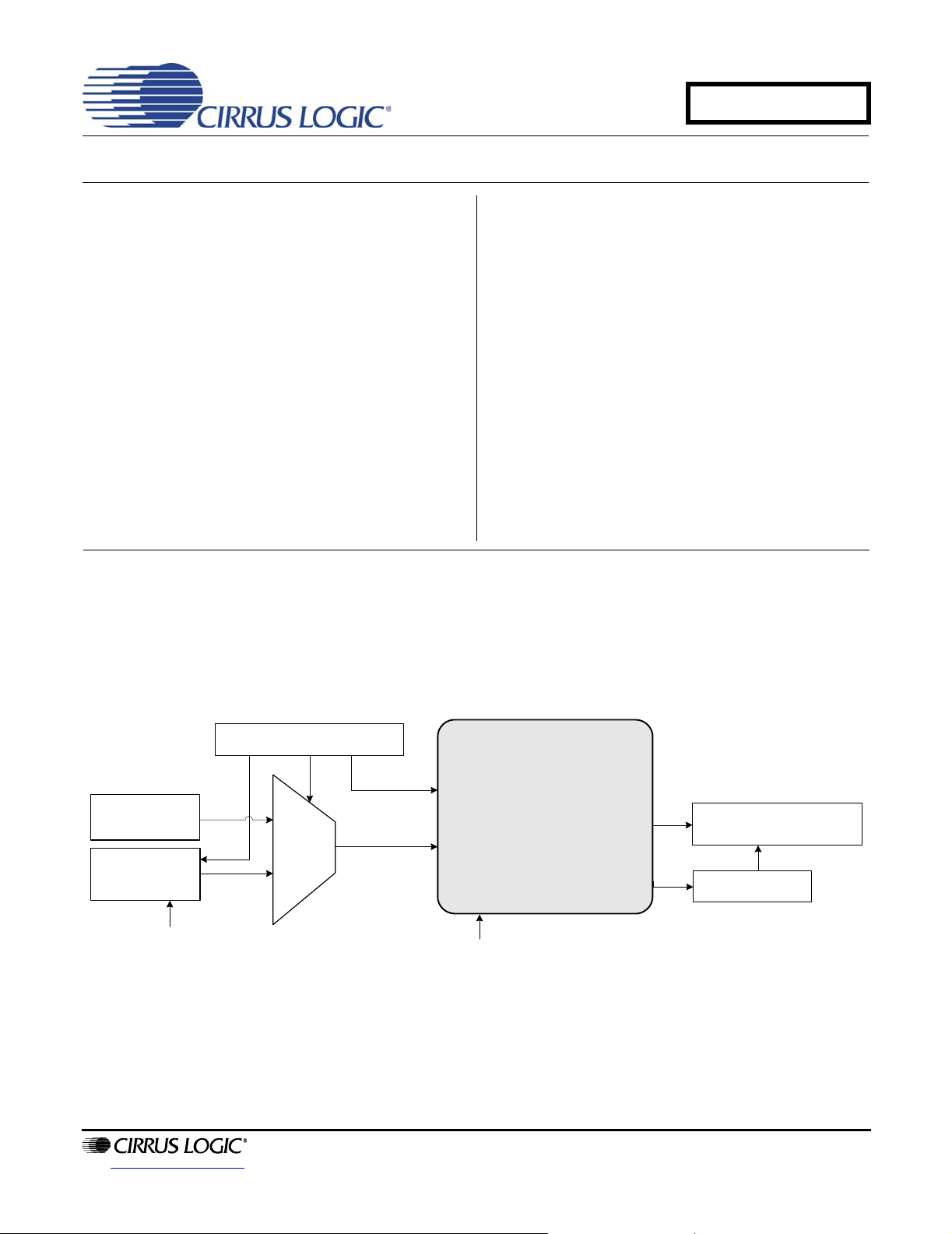
Figure 31. System Block Diagram and Signal Flow .................................................................................. 12
Figure 32. CS4352 .................... ... ....................................................... ...................................................... 13
Figure 33. Analog Outputs ........................................................................................................................ 14
Figure 34. PCM Input Headers .................................................................................................................15
Figure 35. CS8416 S/PDIF Input .............. ... ... ... .... ... ... ... .... ...................................................... ................16
Figure 36. Power ....................................................... ... ... .... ... ...................................................................17
Figure 37. Silkscreen Top ......................................................................................................................... 18
CDB4352
........ 9
2 DS684DB1
Page 3

Figure 38. Top Side ................................................................................................................................... 19
Figure 39. Bottom Side ............................................................................................................................. 20
LIST OF TABLES
Table 1. System Connections .................................................................................................................... 5
Table 2. CDB4352 Jumper Settings .......................................................................................................... 11
CDB4352
DS684DB1 3
Page 4

CDB4352
1. CDB4352 SYSTEM OVERVIEW
The CDB4352 evaluation board is an excellent means of quickly evaluating the CS4352. The CS8416 digital audio
interface receiver provides an easy interface to digi tal audio signal sources including the majority of dig ital audio test
equipment. The evaluation board also allows the u ser to su pply external PCM clo cks and data through a heade r for
system development.
The CDB4352 schematic has been partitioned into five schematics, as shown in Figures32 through 36. Each partitioned schematic is represented in the system diagram shown in Figure 31. Notice that the system diagram also
includes the interconnections between the partitioned schematics.
2. CS4352 DIGITAL-to-ANALOG CONVERTER
A description of the CS4352 is included in the CS4352 datasheet.
3. CS8416 DIGITAL AUDIO RECEIVER
The system receives and decodes the standard S/PDIF data format using a CS8416 Digital Audio Receiver,
Figure 35. The outputs of the CS8416 include a serial bit clock, serial data , left-right clock, and a 128/256 Fs master
clock. The CS8416 data format is fixed to I²S. The operation of the CS8416 and a discussion of the digital audio
interface is included in the CS8416 datasheet.
The evaluation board has been designed such that the input can be either optical or coaxial, see Figure 35. However, both inputs cannot be driven simultaneously.
Position 2 of S1 sets the output MCLK to LRCK ra tio of t he CS8416. Th is switch sho uld be set to 256 (LO) for input
Fs<=48 kHz and can be either 256 (LO) or 128 (HI) for Fs>48 kHz
4. INPUT FOR CLOCKS AND DATA
The evaluation board has been designed to allow interfacing to external systems via the header J13. Header J13
allows the evaluation board to accept externally generated PCM clocks and data. The schematic for the clock/data
input is shown in Figure 34. Switch position 1 of S1 selects the source as either CS8416 or header J13.
Please see the CS4352 datasheet for more information.
5. POWER SUPPLY CIRCUITRY
Power is supplied to the evaluation board by three binding posts (GND, VL, and VA_H), see Figure 36. The VL supply can be jumpered to a +3.3 V regulator or provided externally through the VL binding post. VD and VA is normally
supplied by the 3.3 V regulator but can be disconnected using J4 and J6 and then have external voltage applied to
the VD and VA test points. The +5 V supply (which powers the regulators for this board) is normally supplied by a
5 V regulator but can be supplied externally by removing J7 and applying 5 V to TP8.
Power consumption of the CS4352 can be measured through the voltage drop at J8, J9, J10, and J11 when the
shunts are removed.
WARNING:Refer to the CS4352 datasheet for maximum allowable vo ltages levels. Operation o utside of this range
can cause permanent damage to the device.
4 DS684DB1
Page 5
CDB4352
6. GROUNDING AND POWER SUPPLY DECOUPLING
As with any high-performance converter, the CS4352 requires careful attention to power supply and grounding arrangements to optimize performance. Figure 32 details the connections to the CS4352 and Figures 37, 38, and 39
show the component placement and top and bottom layout. The decoupling capacitors are located as close to the
CS4352 as possible. Extensive use of ground plane fill in the evaluation board yields large reductions in radiated
noise.
7. HARDWARE CONTROL
The CDB4352 is controlled through settings on switch S1. This allows for configuration of the board without a PC.
A switch is provided for CS8416 MCLK speed, clock and data source for the boar d, and the ha rdware mode configuration of the CS4352.
8. ANALOG OUTPUT FILTERING
The analog output on the CDB4352 has been designed according to the CS4352 datasheet. This output circuit includes an AC coupling cap, the BJT mute circuit, and a single-pole R and C.
CONNECTOR INPUT/OUTPUT SIGNAL PRESENT
VL Input + 1.5 V to +3.3 V power for the CS4352 serial interface
VA_H Input
GND Input Ground connection from power supply
SPDIF INPUT - J16 Input Digital audio interface input via coaxial cable
SPDIF INPUT - OPT1 Input Digital audio interface input via optical cable
PCM INPUT - J13 Input Input for master, serial, left/right clocks and serial data
AOUTA and AOUTB Output RCA line-level analog outputs
+9 V to +12 V positive supply for the CS4352 high-voltage analog and
the CDB4352 regulators
Table 1. System Connections
DS684DB1 5
Page 6
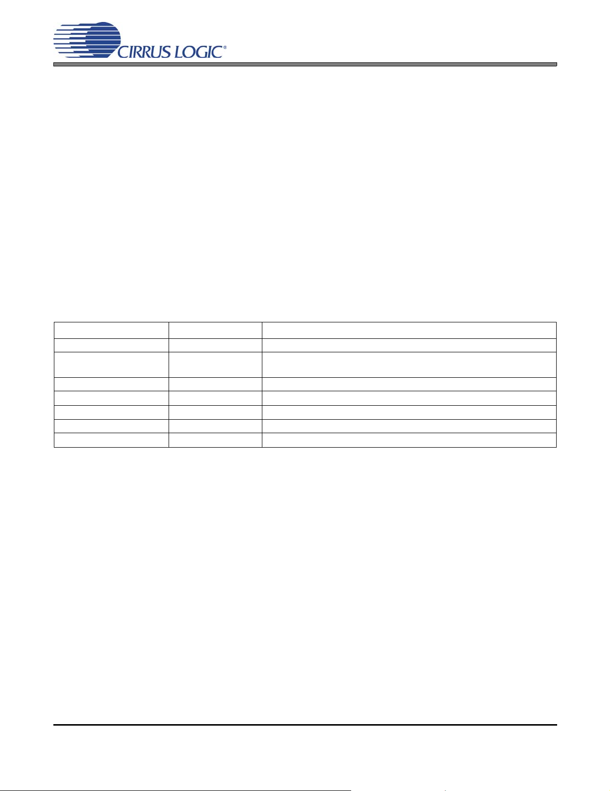
9. PERFORMANCE PLOTS
CDB4352
+0
-10
-20
-30
-40
-50
-60
d
B
-70
r
-80
A
-90
-100
-110
-120
-130
-140
20 20k50 100 200 500 1k 2k 5k 10k
Hz
Figure 1. FFT (48 kHz, 0 dB) Figure 2. FFT (48 kHz, -60 dB)
+0
-10
-20
-30
-40
-50
-60
d
B
-70
r
-80
A
-90
-100
-110
-120
-130
-140
20 20k50 100 200 500 1k 2k 5k 10k
Hz
Figure 3. FFT (48 kHz, No Input) Figure 4. FFT (48 kHz Out-of-Band, No Input)
+0
-10
-20
-30
-40
-50
-60
d
B
-70
r
-80
A
-90
-100
-110
-120
-130
-140
20 20k50 100 200 500 1k 2k 5k 10k
+0
-10
-20
-30
-40
-50
-60
d
B
-70
r
-80
A
-90
-100
-110
-120
-130
-140
20k 120k40k 60k 80k 100k
Hz
Hz
+0
-10
-20
-30
-40
d
-50
B
r
-60
A
-70
-80
-90
-100
-110
20 20k50 100 200 500 1k 2k 5k 10k
Hz
+0
-10
-20
-30
-40
d
-50
B
r
-60
A
-70
-80
-90
-100
-110
-120 +0-100 -80 -60 -40 -20
dBFS
Figure 5. 48 kHz, THD+N vs. Input Freq Figure 6. 48 kHz, THD+N vs. Level
6 DS684DB1
Page 7
CDB4352
+40
+35
+30
+25
+20
+15
+10
d
+5
B
+0
r
-5
A
-10
-15
-20
-25
-30
-35
-40
-140 +0-120 -100 -80 -60 -40 -20
dBFS
+5
+4
+3
+2
+1
d
B
+0
r
A
-1
-2
-3
-4
-5
20 20k50 100 200 500 1k 2k 5k 10k
Hz
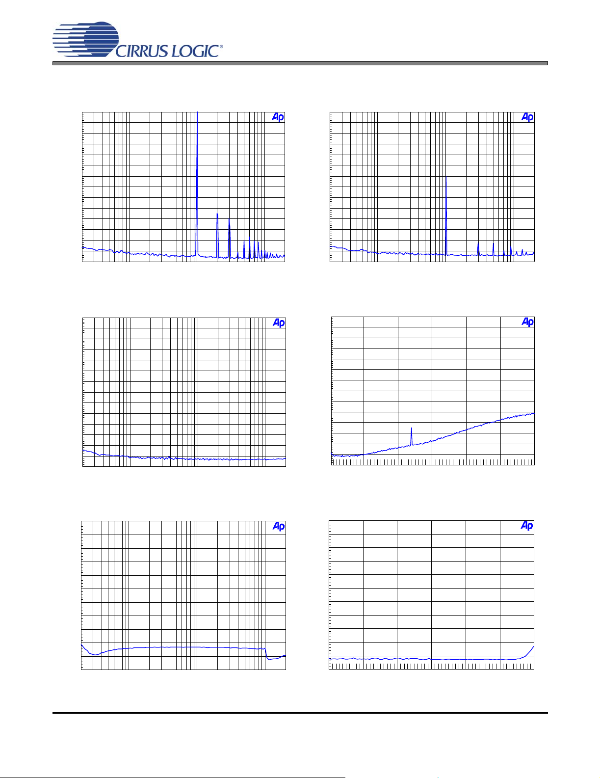
Figure 7. 48 kHz, Fade-to-Noise Linearity Figure 8. 48 kHz, Frequency Response
+0
-10
-20
-30
-40
-50
-60
d
-70
B
-80
-90
-100
-110
-120
-130
-140
20 20k50 100 200 500 1k 2k 5k 10k
Hz
3
2.5
2
1.5
1
500m
0
V
-500m
-1
-1.5
-2
-2.5
-3
0 3m500u 1m 1.5m 2m 2.5m
sec
Figure 9. 48 kHz, Crosstalk Figure 10. 48 kHz, Impulse Response
+0
-10
-20
-30
-40
-50
-60
d
B
-70
r
-80
A
-90
-100
-110
-120
-130
-140
20 20k50 100 200 500 1k 2k 5k 10k
Hz
+0
-10
-20
-30
-40
-50
-60
d
B
-70
r
-80
A
-90
-100
-110
-120
-130
-140
20 20k50 100 200 500 1k 2k 5k 10k
Hz
Figure 11. FFT (96 kHz, 0 dB) Figure 12. FFT (96 kHz, -60 dB)
DS684DB1 7
Page 8

CDB4352
+0
-10
-20
-30
-40
-50
-60
d
B
-70
r
-80
A
-90
-100
-110
-120
-130
-140
20 20k50 100 200 500 1k 2k 5k 10k
Hz
Figure 13. FFT (96 kHz, No Input) Figure 14. FFT (96 kHz Out-of-Band, No Input)
+0
-10
-20
-30
-40
d
-50
B
r
-60
A
-70
-80
-90
-100
-110
20 20k50 100 200 500 1k 2k 5k 10k
Hz
+0
-10
-20
-30
-40
-50
-60
d
B
-70
r
-80
A
-90
-100
-110
-120
-130
-140
+0
-10
-20
-30
-40
d
-50
B
r
-60
A
-70
-80
-90
-100
-110
-120 +0-100 -80 -60 -40 -20
20k 120k40k 60k 80k 100k
Hz
dBFS
Figure 15. 96 kHz, THD+N vs. Input Freq Figure 16. 96 kHz, THD+N vs. Level
+40
+35
+30
+25
+20
+15
+10
d
+5
B
+0
r
-5
A
-10
-15
-20
-25
-30
-35
-40
-140 +0-120 -100 -80 -60 -40 -20
dBFS
+5
+4
+3
+2
+1
d
B
+0
r
A
-1
-2
-3
-4
-5
20 20k50 100 200 500 1k 2k 5k 10k
Hz
Figure 17. 96 kHz, Fade-to-Noise Linearity Figure 18. 96 kHz, Frequency Response
8 DS684DB1
Page 9

CDB4352
+0
-10
-20
-30
-40
-50
-60
d
-70
B
-80
-90
-100
-110
-120
-130
-140
20 20k50 100 200 500 1k 2k 5k 10k
Hz
Figure 19. 96 kHz, Crosstalk Figure 20. 96 kHz, Impulse Response
+0
-10
-20
-30
-40
-50
-60
d
B
-70
r
-80
A
-90
-100
-110
-120
-130
-140
20 20k50 100 200 500 1k 2k 5k 10k
Hz
3
2.5
2
1.5
1
500m
0
V
-500m
-1
-1.5
-2
-2.5
-3
0 1.5m250u 500u 750u 1m 1.25m
+0
-10
-20
-30
-40
-50
-60
d
B
-70
r
-80
A
-90
-100
-110
-120
-130
-140
20 20k50 100 200 500 1k 2k 5k 10k
sec
Hz
Figure 21. FFT (192 kHz, 0 dB) Figure 22. FFT (192 kHz, -60 dB)
+0
-10
-20
-30
-40
-50
-60
d
B
-70
r
-80
A
-90
-100
-110
-120
-130
-140
20 20k50 100 200 500 1k 2k 5k 10k
Hz
+0
-10
-20
-30
-40
-50
-60
d
B
-70
r
-80
A
-90
-100
-110
-120
-130
-140
20k 120k40k 60k 80k 100k
Hz
Figure 23. FFT (192 kHz, No Input) Figure 24. FFT (192 kHz Out-of-Band, No Input)
DS684DB1 9
Page 10

CDB4352
+0
-10
-20
-30
-40
d
-50
B
r
-60
A
-70
-80
-90
-100
-110
20 20k50 100 200 500 1k 2k 5k 10k
Hz
+0
-10
-20
-30
-40
d
-50
B
r
-60
A
-70
-80
-90
-100
-110
-120 +0-100 -80 -60 -40 -20
dBFS
Figure 25. 192 kHz, THD+N vs. Input Freq Figure 26. 192 kHz, THD+N vs. Level
+40
+35
+30
+25
+20
+15
+10
d
+5
B
+0
r
-5
A
-10
-15
-20
-25
-30
-35
-40
-140 +0-120 -100 -80 -60 -40 -20
dBFS
+5
+4
+3
+2
+1
d
B
+0
r
A
-1
-2
-3
-4
-5
20 20k50 100 200 500 1k 2k 5k 10k
Hz
Figure 27. 192 kHz, Fade-to-Noise Linearity Figure 28. 192 kHz, Frequency Response
+0
-10
-20
-30
-40
-50
-60
d
-70
B
-80
-90
-100
-110
-120
-130
-140
20 20k50 100 200 500 1k 2k 5k 10k
Hz
3
2.5
2
1.5
1
500m
0
V
-500m
-1
-1.5
-2
-2.5
-3
0 600u200u 400u
sec
Figure 29. 192 kHz, Crosstalk Figure 30. 192 kHz, Impulse Response
10 DS684DB1
Page 11

CDB4352
JUMPER /
SWITCH PURPOSE POSITION FUNCTION SELECTED
J7
J4
J5
J6
J8 Current measure for VD *shunted
J9 Current measure for VL *shunted
J10 Current measure for VA *shunted
J11 Current measure for VA_H *shunted
S1
S2 Reset - Enables reset for CS4352 and CS8416 when pressed
J12
J17
Selects source of voltage for
the +5V supplies
Selects source of voltage for
the VD supplies
Selects source of voltage for
the VL supply
Selects source of voltage for
the VA supply
Sets clock source, CS8416
clock speed, and CS4352 set-
tings
Mute Disable
+5 V
*+5V_REG
VD
*+3.3V REG
VL
*+3.3V REG
VA
*+3.3V REG
*1 = open
*2, 3, 4, 5 = closed
*LED
MUTE
Voltage source is +5 V test point (TP8)
Voltage source is +5 V regulator
Voltage sourc e is VD test point (TP2)
Voltage source is +3.3 V regulator
Voltage source is VL binding post
Voltage source is +3.3 V regulator
Voltage source is VA test point (TP7)
Voltage source is +3.3 V regulator
When shunt is removed, the voltage can be measured
across a fixed resistance to determine current.
When shunt is removed, the voltage can be measured
across a fixed resistance to determine current.
When shunt is removed, the voltage can be measured
across a fixed resistance to determine current.
When shunt is removed, the voltage can be measured
across a fixed resistance to determine current.
position 1: 0 = external clock source, 1 = CS8416
position 2: 0 = 8416 MCLK is 256xFs, 1 = 128xFs
Position 3,4,5: see CS4352 datasheet
Bypasses muting to turn on LED
Normal muting circuit
Table 2. CDB4352 Jumper Settings
*Default Factory Settings.
10.DESIGN NOTE
10.1 CDB4352 Revision A.0
D2 has been removed and shorted and R2 has been removed.
The serial audio decode table for S1 is incorrect. ‘01’ should be RJ-24 and ‘10’ should be LJ
The polarity of the silkscreen for Z1, Z2, Z3, Z4, and Z5 is incorrect
The CS4352 revision is A1
10.2 CDB4352 Revision B.0
No errors at this time
DS684DB1 11
Page 12

12 DS684DB1
11.SCHEMATICS
8416 Digital
Audio Receiver
Figure 35
PCM Inputs
Figure 34
MCLK
SCLK
LRCK
SDIN
Reset
Circuit
Hardware Switch
Figure 34
CS4352
Figure 32
Power
Figure 36
Channel A
Outputs and Mute
Figure 33
Channel B
Outputs and Mute
Figure 33
Figure 31. System Block Diagram and Signal Flow
CDB4352
Page 13

DS684DB1 13
Figure 32. CS4352
CDB4352
Page 14
14 DS684DB1
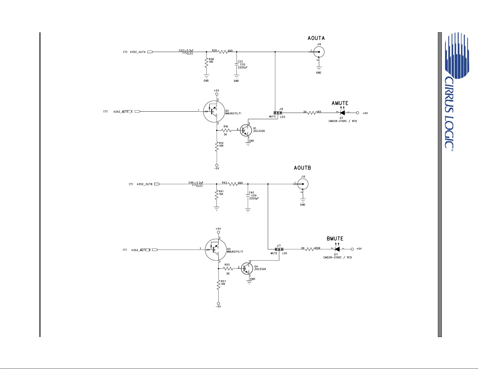
Figure 33. Analog Outputs
CDB4352
Page 15

DS684DB1 15
Figure 34. PCM Input Headers
CDB4352
Page 16

16 DS684DB1
Figure 35. CS8416 S/PDIF Input
CDB4352
Page 17

DS684DB1 17
Figure 36. Power
CDB4352
Page 18

DS684DB1 18
Figure 37. Silkscreen Top
CDB4352
Page 19

19 DS684DB1
Figure 38. Top Side
CDB4352
Page 20

20 DS684DB1
Figure 39. Bottom Side
CDB4352
Page 21

12.REVISION HISTORY
Release Changes
DB1 Initial Release
DB2 Added Performance Plots
CDB4352
Contacting Cirrus Logic Support
For all product questions and inquiries, contact a Cirrus Logic Sales Representative.
To find the one nearest you, go to www.cirrus.com.
IMPORTANT NOTICE
Cirrus Logic, Inc. and its subsidiaries ("Cirrus") believe that the information contained in this document is accurate and reliable. However, the information is subject
to change without not ice and is pr ovided "AS IS" witho ut warr anty of any kind (express or implied). Customers are advised to obtain the latest version of relevant
information to verify, before placing orders, that information being relied on is current and complete. All products are sold subject to the terms and conditions of sale
supplied at the time of order acknowledgment, including those pertaining to warranty, indemnification, and limitation of liability. No responsibility is assumed by Cirrus
for the use of this information, including use of this information as the basis for manufacture or sale of any items, or for infringement of patents or other rights of third
parties. This document is the property of Cirrus and by furnishing this information, Cirrus grants no license, express or implied under any patents, mask work rights,
copyrights, trademarks, trade secrets or other inte llectual property rig hts. Cirrus owns the copyrights associated with the information contained herein and gives consent for copies to be made of the information only for use within your organization with respect to Cirrus integrated circuits or other products of Cirrus. This consent
does not extend to other copying such as copying for general distribution, advertising or promotional purposes, or for creating any work for resale.
CERTAIN APPLICATIONS USING SEMICONDUCTOR PRODUCTS MAY INVOLVE POTENTIAL RISKS OF DEATH, PERSONAL INJURY, OR SE VERE PROPERTY OR ENVIRONMENTAL DAMAGE (“CRITICAL APPLICATIONS”). CIRRUS PRODUCTS ARE NOT DESIGNED, AUTHORIZED OR WARRANTED FOR USE
IN AIRCRAFT SYSTEMS, MILITARY APPLICATIONS, PRODUCTS SURGICALLY IMPLANTED INTO THE BODY, AUTOMOTIVE SAFETY OR SECURITY DEVICES, LIFE SUPPORT PRODUCTS OR OTHER CRITICAL APPLICATIONS. INCLUSION OF CIRRUS PRODUCTS IN SUCH APPLICATIONS IS UNDERSTOOD TO BE FULLY AT THE CUSTOMER’S RISK AND CIRRUS DISCLAIMS AND MAKES NO WARRANTY, EXPRESS, STATUTORY OR IMPLIED,
INCLUDING THE IMPLIED WARRANTIES OF MERCHANTABILITY AND FITNESS FOR PARTICULAR PURPOSE, WITH REGARD TO ANY CIRRUS PRODUCT
THAT IS USED IN SUCH A MANNER. IF THE CUSTOMER OR CUSTOMER’S CUSTOMER USES OR PERMITS THE USE OF CIRRUS PRODUCTS IN CRITICAL
APPLICATIONS, CUSTOMER AGREES, BY SUCH USE, T O FULLY INDEMNIF Y CIRRUS, ITS OF FICE RS, DI RECTORS, EMPLOYEES, DISTRI BUTORS AND
OTHER AGENTS FROM ANY AND ALL LIABILITY, INCLUDING ATTORNEYS’ FEES AND COSTS, THAT MAY RESULT FROM OR ARISE IN CONNECTION
WITH THESE USES.
Cirrus Logic, Cirrus, and the Cirrus Logic logo designs are trademarks of Cirrus Logic, Inc. All other brand and product names in this document may be trademarks
or service marks of their respective owners.
DS684DB1 21
 Loading...