

Page 1
Evaluation Board for CS4349
CDB4349
Features
Stand-Alone or PC GUI Board Control
CS8416 Receives S/PDIF-Compatible Digital
Audio
Headers for External PCM Audio Input
Demonstrates Recommended Layout and
Grounding Arrangements.
Requires Only a Digital Signal Source and
Power Supplies for a Complete Digital-toAnalog Converter System
Description
The CDB4349 evaluation board is an excellent platform
for quickly evaluating the CS4349 24-bit, 24-pin, stereo
D/A converter. Evaluation requires an analog signal analyzer, a digital signal source, a PC for controlling the
CS4349 (only required for Control Port Mode), and a
power supply. Analog line-level outputs are provided via
RCA phono jacks.
The CS8416 digital audio rec eiver IC provide s the sy stem timing necessary to operate the digital-to-analog
converter and will accept S/PDIF-compatible audio data. The evaluation board may also be configured to
accept external timing and data signals for operation in
a user application during system development.
ORDERING INFORMATION
CDB4349 Evaluation Board
Inputs for PCM
Clocks and Data
CS8416
Digital Audio
Interface
http://www.cirrus.com
Hardware or
Software Board
Control
CS4349
Copyright © Cirrus Logic, Inc. 2008
(All Rights Reserved)
Analog Outputs
and Filtering
JUN '08
DS782DB1
Page 2

TABLE OF CONTENTS
1. CDB4349 SYSTEM OVERVIEW ............................................................................................................ 4
2. CS4349 DIGITAL-TO-ANALOG CONVERTER ..................................................................................... 4
3. CS8416 DIGITAL AUDIO RECEIVER .................................................................................................... 4
4. INPUT FOR CLOCKS AND DATA ......................................................................................................... 4
5. INPUT FOR CONTROL DATA ............................................................................................................... 4
6. POWER SUPPLY CIRCUITRY ............................................................................................................... 5
7. GROUNDING AND POWER SUPPLY DECOUPLING .......................................................................... 5
8. ANALOG OUTPUT FILTERING ................. ... .... ... ... ... .... ... ....................................... ... ... ... ... .... ... ........... 5
9. BOARD CONNECTIONS AND SETTINGS ............................................................................................ 6
10. PERFORMANCE PLOTS ..................................................................................................................... 7
11. SCHEMATICS .................................................................................................................................... 13
12. LAYOUT ............................................................................................................................................. 20
13. REVISION HISTORY .......................................................................................................................... 23
LIST OF FIGURES
Figure 1. FFT 0 dBFS, FS = 48 kHz ...................... ... ... ... .... ... ... ... .... ... ... ....................................... ... ........... 7
Figure 2. FFT -60 dBFS, FS = 48 kHz ................... ... .......................................... ... ... .... ... ... ... ..................... 7
Figure 3. FFT No Input, FS = 48 kHz ........ ... ... ... .... ... ... ... .... .......................................... ... ........................... 7
Figure 4. FFT No Input Out of Band, FS = 48 kHz ....... ... .... ... ... ... .... ... ... ... ... .... ... ... ... .................................. 7
Figure 5. Frequency Response 0 dBFS, FS = 48 kHz ................................................................................ 7
Figure 6. THD+N vs Frequency 0 dBFS, FS = 48 kHz ............................................................................... 7
Figure 7. THD+N vs Level 1 kHz, FS = 48 kHz ........................................................................................... 8
Figure 8. Fade-to-Noise Linearity 1 kHz, FS = 48 kHz ...............................................................................8
Figure 9. Impulse Response, FS = 48 kHz ................................................................................................. 8
Figure 10. FFT Crosstalk Ch. A to Ch. B 1 kHz, FS = 48 kHz ......................................................... ........... 8
Figure 11. FFT Crosstalk Ch. B to Ch. A 1 kHz, FS = 48 kHz ......................................................... ........... 8
Figure 12. FFT 0 dBFS, FS = 96 kHz ......................................................................................................... 8
Figure 13. FFT -60 dBFS, FS = 96 kHz ...................................................................................................... 9
Figure 14. FFT No Input, FS = 96 kHz ........................................................................................................ 9
Figure 15. FFT No Input Out of Band, FS = 96 kHz .................................................................................... 9
Figure 16. Frequency Response 0 dBFS, FS = 96 kHz .............................................................................. 9
Figure 17. THD+N vs Frequency 0 dBFS, FS = 96 kHz . .... ... ... ... .......................................... ... .... ... ... ... .... . 9
Figure 18. THD+N vs Level 1 kHz, FS = 96 kHz ............. .... ... .......................................... ... ... ... .... ... ... ... ..... 9
Figure 19. Fade-to-Noise Linearity 1 kHz, FS = 96 kHz ........................................................................... 10
Figure 20. Impulse Response, FS = 96 kHz ............................................................................................. 10
Figure 21. FFT Crosstalk Ch. A to Ch. B 1 kHz, FS = 96 kHz ......................................................... ......... 10
Figure 22. FFT Crosstalk Ch. B to Ch. A 1 kHz, FS = 96 kHz ......................................................... ......... 10
Figure 23. FFT 0 dBFS, FS = 192 kHz ..................................................................................................... 10
Figure 24. FFT -60 dBFS, FS = 192 kHz .................................................................................................. 10
Figure 25. FFT No Input, FS = 192 kHz ............................................................................................
Figure 26. FFT No Input Out of Band, FS = 192 kHz ................................................................................ 11
Figure 27. Frequency Response 0 dBFS, FS = 192 kHz .......................................................................... 11
Figure 28. THD+N vs Frequency 0 dBFS, FS = 192 kHz ... ... ... ... .... ... ... ... ... .... ... ... ... .... ... ... ... ... .... ... ... ... ... 11
Figure 29. THD+N vs Level 1 kHz, FS = 192 kHz ........ ... .... ... ... ... .... ... ... ... ... .... ... ... ... ................................ 11
Figure 30. Fade-to-Noise Linearity 1 kHz, FS = 192 kHz ......................................................................... 11
Figure 31. Impulse Response, FS = 192 kHz ........................................................................................... 12
Figure 32. FFT Crosstalk Ch. A to Ch. B 1 kHz, FS = 192 kHz ................................................................ 12
Figure 33. FFT Crosstalk Ch. B to Ch. A 1 kHz, FS = 192 kHz ................................................................ 12
Figure 34. System Block Diagram and Signal Flow .................................................................................. 13
Figure 35. CS4349 ....... ...................................... .... ... ... ... .... ... ... ... .... ... ...................................................... 14
Figure 36. Analog Outputs ........................................................................................................................ 15
Figure 37. PCM Input Header and Hardware Control ......................................................... ... ... .... ... .........16
CDB4349
........ 11
2 DS782DB1
Page 3

Figure 38. CS8416 S/PDIF Input .............................................................................................................. 17
Figure 39. Control Port .............................................................................................................................. 18
Figure 40. Power ....................................................................................................................................... 19
Figure 41. Silkscreen Top ......................................................................................................................... 20
Figure 42. Top Side ................................................................................................................................... 21
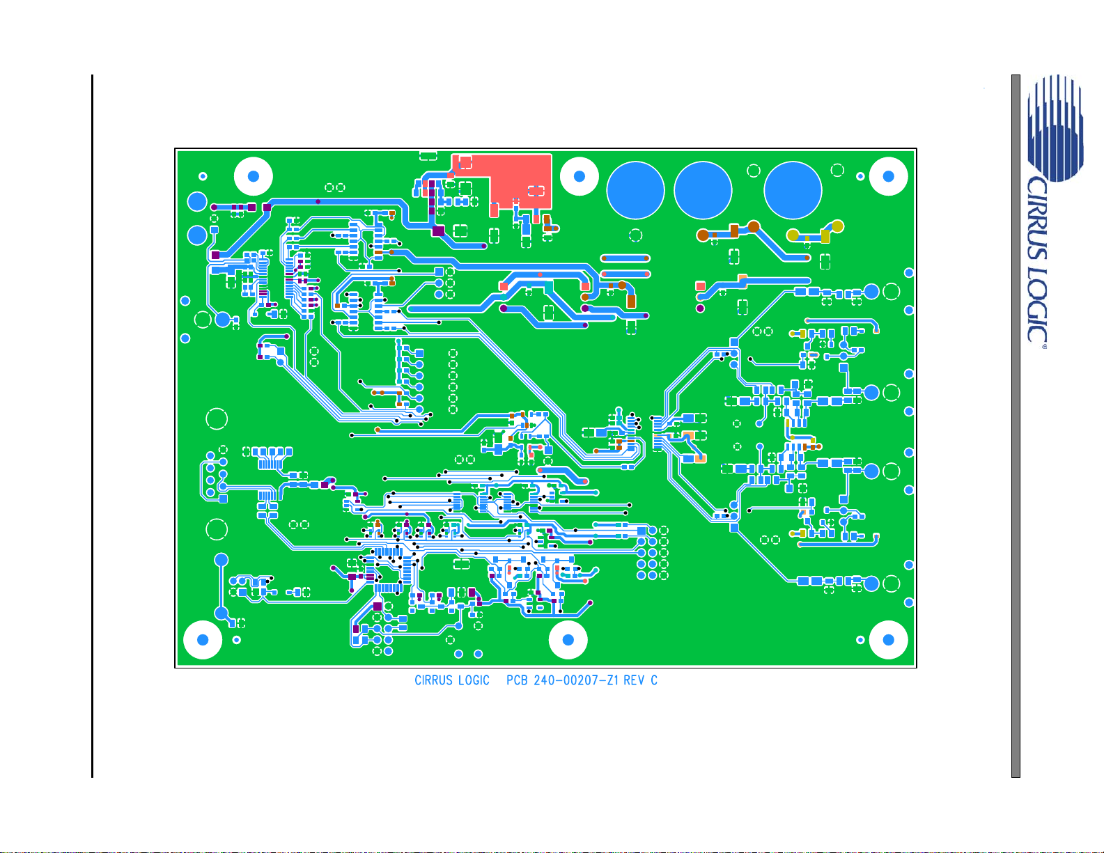
Figure 43. Bottom Side ............................................................................................................................. 22
LIST OF TABLES
Table 1. System Connections ...................................... ... .... ... ... ... .... ... ... ... .................................................. 6
Table 2. CDB4349 Jumper Settings ............................................................................................................ 6
Table 3. CDB4349 Switch Settings ............................................................................................................. 6
CDB4349
DS782DB1 3
Page 4

CDB4349
1. CDB4349 SYSTEM OVERVIEW
The CDB4349 evaluation board is an excellent platform for quickly evaluating the CS4349. The CS8416 digital audio
interface receiver provides an easy interface to digi tal audio signal sources including the majority of dig ital audio test
equipment. The evaluation board also allows the user to supply external PCM clocks and data through head ers for
system development.
The CDB4349 schematic has been partitioned into 6 pages, shown in Figures 35 through 40. Each schematic page
is represented in the system diagram shown in Figure 34. Notice that the system diagram also includes the interconnections between the partitioned schematics.
2. CS4349 DIGITAL-TO-ANALOG CONVERTER
A description of the CS4349 is included in the CS4349 datasheet, available at http://www.cirrus.com/en/prod-
ucts/pro/detail/P1116.html.
3. CS8416 DIGITAL AUDIO RECEIVER
The system receives and decodes the standard S/PDIF data format using a CS8416 digital audio receiver
(Figure 38). The outputs of the CS8416 include a serial bit clock, serial data, and a left-right clock. The CS8416 data
format is selected through switch S1. The operation of the CS8416 and a d iscussion of th e digital au dio interface is
included in the CS8416 datasheet, available at http://www.cirrus.com/en/products/pro/detail/P1005.html.
The CDB4349 has been designed so that the input can be either optical or coaxial (see Figure 39). However, both
inputs cannot be driven simultaneously.
After the CS8416 serial format is changed either through S1 in Stand-Alone Mode, or though the CDB4349 GUI in
PC Mode, a reset is required. The CS8416 can b e manually reset using ‘HARDWARE RESET ’ (S2) in Stan d-Alone
Mode, or through software when operating the CDB4349 in PC Mode.
4. INPUT FOR CLOCKS AND DATA
The evaluation board has been designed to allow external PCM data input through header J10. The schematic for
the clock/data input is shown in Figure 37. In Stand-Alone Mode, switch position 6 of S4 selects the source as either
CS8416 (open) or header J10 (closed). In PC Mode, the PCM source is selected through software.
5. INPUT FOR CONTROL DATA
The evaluation board can be run in either a Stand-Alone Mode or with a PC. Stand-Alone Mode does not require
the use of a PC, and the mode pins are configured using switch positions 1 through 5 of S4 and switch positions 1
and 2 of S1. PC Mode uses software to set up the CS4349 through I²C
or USB port. When the serial port (RS232) or USB is attached and the CDB4349 software is running, PC Mode is
automatically selected.
Header J38 offers the option for external input of RST and SPI/I²C clocks and data. The board is set up from the
factory to use the on-board microcontroller in conjunction with software available at http://www.cirrus.com/en/prod-
ucts/software/msaudio.html. To use an external control source, rem ove the shunts on J3 8 and place a ribbon ca ble
so the signal lines are on the center row and the grounds are on the right side. R89 and R90 should be populated
with 2 kΩ resistors when using an external I²C source which does not already provide pull-ups.
®
or SPI™ interface using the PC’s serial port
4 DS782DB1
Page 5

CDB4349
6. POWER SUPPLY CIRCUITRY
Power is supplied to the evaluation board by three binding posts (GND, +12V, and -12V), as shown in Figure 40.
The ‘+12V’ and ‘-12V’ terminals supply the active output filters. The +3.3 V and +5.0 V circuitry is powered by regulators fed by the ‘+12V’ terminal. Headers J3, J4, and J7 allow the user to either select +3.3 V or +5.0 V supplies
for the various CS4349 voltage supply pins. Alternatively, the user can remove the shunts on J3, J4, and J7, and
provide an external power supply.
WARNING:Refer to the CS4349 datasheet for maximum allowable voltage levels. Operation outside of this range
can cause permanent damage to the device.
7. GROUNDING AND POWER SUPPLY DECOUPLING
As with any high-performance converter, the CS4349 requires careful attention to power supply and grounding arrangements in order to optimize performance. Figure 35 details the connections to the CS4349 while Figures 41,
42, and 43 show the component placement and top and bottom layout. The decoupling capacitors are located as
close to the CS4349 as possible. Extensive use of ground plane fill in the evaluation board yields large reductions
in radiated noise.
8. ANALOG OUTPUT FILTERING
The passive output filter on the CDB4349 has been designed according to the CS4349 datasheet.
DS782DB1 5
Page 6
9. BOARD CONNECTIONS AND SETTINGS
Board connections and settings are shown in Table 1, Table 2, and Table 3.
CONNECTOR INPUT/OUTPUT SIGNAL PRESENT
GND Input Ground connection from power supply
+12V Input +12 V positive supply for the on-board filtering
-12V Input -12 V negative supply for the on-board filtering
S/PDIF IN - J1 Input Digital audio interface input via coax
S/PDIF IN - OPT1 Input Digital audio interface input via optical
PCM INPUT - J10 Input Input for master, serial, left/right clocks and serial data
POUTA, POUTB Output RCA line level analog outputs from passive output stage
Table 1. System Connections
JUMPER PURPOSE POSITION FUNCTION SELECTED
J3, J4, J7
J38 Selects source of control data
J27 C2 micro programming - Reserved for factory use only
Selects Supply Voltage for
CS4349
+5V
*+3.3V
*PC CONTROL
shunts removed
Supplies +5.0 V to associated CS4349 supply
*Supplies +3.3 V to associated CS4349 supply
*Control from PC and on-board microcontroller
External control input using center and right columns
CDB4349
Table 2. CDB4349 Jumper Settings
*Default Factory Settings.
SWITCH
(Note 1) PURPOSE POSITION FUNCTION SELECTED
S2 Resets CS8416 and CS4349 The CS8416 must be reset if switch S1 is changed
S1
S4
CS8416 Format Select
SFSEL[1:0]
CS4349 Format Select
DIF[2:0]
CS4349 De-emphasis Select 4
®
CS4349 Popguard
Selects PCM source for
CS4349
Enable 5
Table 3. CDB4349 Switch Settings
1, 2
1, 2, 3
6
Default: SFSEL[1:0] = 00 (Closed). See CS8416 datasheet
for details.
Default: DIF[2:0] = 000 (Closed). See CS4349 datasheet
for details.
open = De-emphasis enabled
*closed = De-emphasis disabled.
open = Popguard enabled
*closed = Popguard disabled.
*open = CS8416
closed = PCM Header J10
*Default Factory Settings.
Note:
1. Switch settings take effect in Stand-Alone Mode only.
6 DS782DB1
Page 7
CDB4349
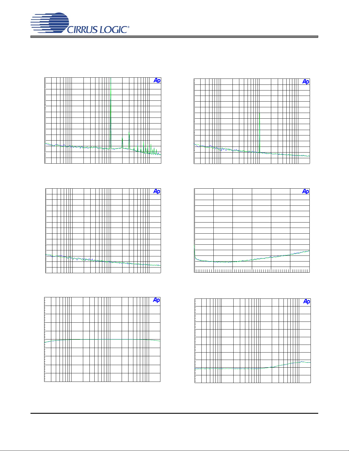
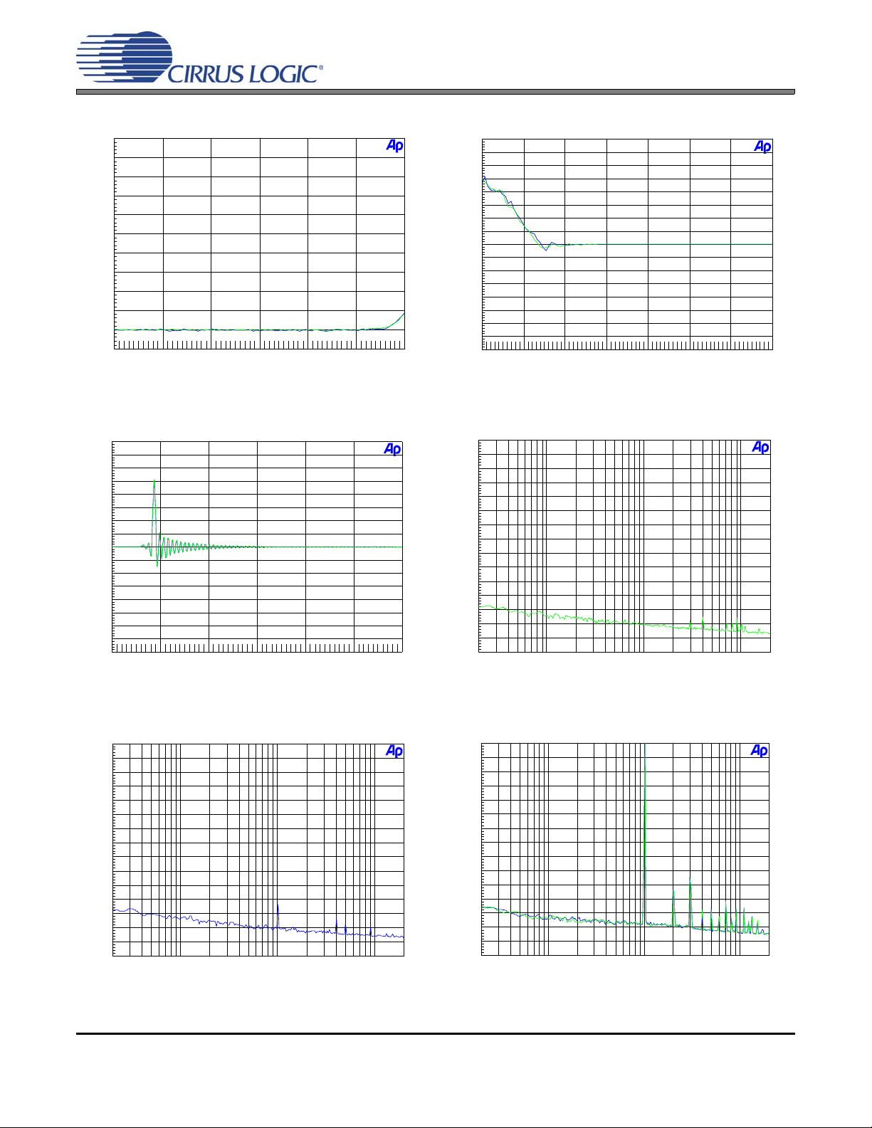
10.PERFORMANCE PLOTS
Test conditions (unless otherwise specified): TA= 25° C; Measurement bandwidth is 20 Hz to 20 kHz (unweighted);
VA = 5 V; VLC = VLS = 3.3 V; Input signal is a 0 dBFS 1 kHz sine wave; Input data resolution is 24 bits, Left-Justified; Channel A output = blue traces; Channel B output = green traces.
+0
-10
-20
-30
-40
-50
-60
d
-70
B
r
-80
A
-90
-100
-110
-120
-130
-140
-150
20 20k50 100 200 500 1k 2k 5k 10k
Hz
Figure 1. FFT 0 dBFS, FS = 48 kHz Figure 2. FFT -60 dBFS, FS = 48 kHz
+0
-10
-20
-30
-40
-50
-60
d
-70
B
r
-80
A
-90
-100
-110
-120
-130
-140
-150
20 20k50 100 200 500 1k 2k 5k 10k
Hz
+0
-10
-20
-30
-40
-50
-60
d
B
-70
r
-80
A
-90
-100
-110
-120
-130
-140
-150
20 20k50 100 200 500 1k 2k 5k 10k
Hz
+0
-10
-20
-30
-40
-50
-60
d
B
-70
r
-80
A
-90
-100
-110
-120
-130
-140
-150
20k 120k40k 60k 80k 100k
Hz
Figure 3. FFT No Input, FS = 48 kHz Figure 4. FFT No Input Out of Band, FS = 48 kHz
+5
+4
+3
+2
+1
d
B
+0
r
A
-1
-2
-3
-4
-5
20 20k50 100 200 500 1k 2k 5k 10k
Hz
+0
-10
-20
-30
-40
d
-50
B
r
-60
A
-70
-80
-90
-100
-110
20 20k50 100 200 500 1k 2k 5k 10k
Hz
Figure 5. Frequency Response 0 dBFS, FS = 48 kHz Figure 6. THD+N vs Frequency 0 dBFS, FS = 48 kHz
DS782DB1 7
Page 8
CDB4349
+0
-10
-20
-30
-40
d
-50
B
r
-60
A
-70
-80
-90
-100
-110
-120 +0-100 -80 -60 -40 -20
dBFS
+40
+35
+30
+25
+20
+15
+10
d
+5
B
+0
r
-5
A
-10
-15
-20
-25
-30
-35
-40
-140 +0-120 -100 -80 -60 -40 -20
dBFS
Figure 7. THD+N vs Level 1 k Hz, FS = 48 kHz Figure 8. Fade-to-Noise Linearity 1 kHz, FS = 48 kHz
2
1.75
1.5
1.25
1
750m
500m
250m
0
V
-250m
-500m
-750m
-1
-1.25
-1.5
-1.75
-2
0 3m500u1m1.5m2m2.5m
sec
+0
-10
-20
-30
-40
-50
-60
d
B
-70
r
-80
A
-90
-100
-110
-120
-130
-140
-150
20 20k50 100 200 500 1k 2k 5k 10k
Hz
Figure 9. Impulse Response, FS = 48 kHz Figure 10. FFT Crosstalk Ch. A to Ch. B 1 kHz,
FS = 48 kHz
+0
-10
-20
-30
-40
-50
-60
d
B
-70
r
-80
A
-90
-100
-110
-120
-130
-140
-150
20 20k50 100 200 500 1k 2k 5k 10k
Hz
Figure 11. FFT Crosstalk Ch. B to Ch. A 1 kHz,
+0
-10
-20
-30
-40
-50
-60
d
B
-70
r
-80
A
-90
-100
-110
-120
-130
-140
-150
20 20k50 100 200 500 1k 2k 5k 10k
Hz
Figure 12. FFT 0 dBFS, FS = 96 kHz
FS = 48 kHz
8 DS782DB1
Page 9

CDB4349
+0
-10
-20
-30
-40
-50
-60
d
-70
B
r
-80
A
-90
-100
-110
-120
-130
-140
-150
20 20k50 100 200 500 1k 2k 5k 10k
Hz
Figure 13. FFT -60 dBFS, FS = 96 kHz Figure 14. FFT No Input, FS = 96 kHz
+0
-10
-20
-30
-40
-50
-60
d
B
-70
r
-80
A
-90
-100
-110
-120
-130
-140
-150
20k 120k40k 60k 80k 100k
Hz
+0
-10
-20
-30
-40
-50
-60
d
-70
B
r
-80
A
-90
-100
-110
-120
-130
-140
-150
20 20k50 100 200 500 1k 2k 5k 10k
+5
+4
+3
+2
+1
d
B
+0
r
A
-1
-2
-3
-4
-5
20 20k50 100 200 500 1k 2k 5k 10k
Hz
Hz
Figure 15. FFT No Input Out of Band, FS = 96 kHz Figure 16. Frequency Response 0 dBFS, FS = 96 kHz
+0
-10
-20
-30
-40
d
-50
B
r
-60
A
-70
-80
-90
-100
-110
20 20k50 100 200 500 1k 2k 5k 10k
Hz
+0
-10
-20
-30
-40
d
-50
B
r
-60
A
-70
-80
-90
-100
-110
-120 +0-100 -80 -60 -40 -20
dBFS
Figure 17. THD+N vs Frequency 0 dBFS, FS = 96 kHz Figure 18. THD+N vs Level 1 kHz, FS = 96 kHz
DS782DB1 9
Page 10

CDB4349
+40
+35
+30
+25
+20
+15
+10
d
+5
B
+0
r
-5
A
-10
-15
-20
-25
-30
-35
-40
-140 +0-120 -100 -80 -60 -40 -20
dBFS
2
1.75
1.5
1.25
1
750m
500m
250m
0
V
-250m
-500m
-750m
-1
-1.25
-1.5
-1.75
-2
0 1.5m250u 500u 750u 1m 1.25m
sec
Figure 19. Fade-to-Noise Linearity 1 kHz, FS = 96 kHz Figure 20. Impulse Response, FS = 96 kHz
+0
-10
-20
-30
-40
-50
-60
d
-70
B
r
-80
A
-90
-100
-110
-120
-130
-140
-150
20 20k50 100 200 500 1k 2k 5k 10k
Hz
+0
-10
-20
-30
-40
-50
-60
d
-70
B
r
-80
A
-90
-100
-110
-120
-130
-140
-150
20 20k50 100 200 500 1k 2k 5k 10k
Hz
Figure 21. FFT Crosstalk Ch. A to Ch. B 1 kHz,
FS = 96 kHz
+0
-10
-20
-30
-40
-50
-60
d
-70
B
r
-80
A
-90
-100
-110
-120
-130
-140
-150
20 20k50 100 200 500 1k 2k 5k 10k
Hz
Figure 22. FFT Crosstalk Ch. B to Ch. A 1 kHz,
FS = 96 kHz
+0
-10
-20
-30
-40
-50
-60
d
-70
B
r
-80
A
-90
-100
-110
-120
-130
-140
-150
20 20k50 100 200 500 1k 2k 5k 10k
Hz
Figure 23. FFT 0 dBFS, FS = 192 kHz Figure 24. FFT -60 dBFS, FS = 192 kHz
10 DS782DB1
Page 11

CDB4349
+0
-10
-20
-30
-40
-50
-60
d
-70
B
r
-80
A
-90
-100
-110
-120
-130
-140
-150
20 20k50 100 200 500 1k 2k 5k 10k
Hz
Figure 25. FFT No Input, FS = 192 kHz Figure 26. FFT No Input Out of Band, FS = 192 kHz
+5
+4
+3
+2
+1
d
B
+0
r
A
-1
-2
-3
-4
-5
20 20k50 100 200 500 1k 2k 5k 10k
Hz
+0
-10
-20
-30
-40
-50
-60
d
-70
B
r
-80
A
-90
-100
-110
-120
-130
-140
-150
+0
-10
-20
-30
-40
d
-50
B
r
-60
A
-70
-80
-90
-100
-110
20 20k50 100 200 500 1k 2k 5k 10k
20k 120k40k 60k 80k 100k
Hz
Hz
Figure 27. Frequency Response 0 dBFS, FS = 192 kHz Figure 28. THD+N vs Frequency 0 dBFS, FS = 192 kHz
+0
-10
-20
-30
-40
d
-50
B
r
-60
A
-70
-80
-90
-100
-110
-120 +0-100 -80 -60 -40 -20
dBFS
+40
+35
+30
+25
+20
+15
+10
d
+5
B
+0
r
-5
A
-10
-15
-20
-25
-30
-35
-40
-140 +0-120 -100 -80 -60 -40 -20
dBFS
Figure 29. THD+N vs Level 1 kHz, FS = 192 kHz Figure 30. Fade-to-Noise Linearity 1 kHz, FS = 192 kHz
DS782DB1 11
Page 12

CDB4349
2
1.75
1.5
1.25
1
750m
500m
250m
0
V
-250m
-500m
-750m
-1
-1.25
-1.5
-1.75
-2
0 600u200u 400u
sec
+0
-10
-20
-30
-40
-50
-60
d
-70
B
r
-80
A
-90
-100
-110
-120
-130
-140
-150
20 20k50 100 200 500 1k 2k 5k 10k
Hz
Figure 31. Impulse Response, FS = 192 kHz Figure 32. FFT Crosstalk Ch. A to Ch. B 1 kHz,
FS = 192 kHz
+0
-10
-20
-30
-40
-50
-60
d
-70
B
r
-80
A
-90
-100
-110
-120
-130
-140
-150
20 20k50 100 200 500 1k 2k 5k 10k
Hz
Figure 33. FFT Crosstalk Ch. B to Ch. A 1 kHz,
FS = 192 kHz
12 DS782DB1
Page 13

DS782DB1 13
11.SCHEMATICS
PCM Header
Figure 3
PCM Clocks/Data
Se rial Con tro l Port
PCM source select
Figure 3
Power
I2C/SPI Header
Figure 4
Figure 3
CS8416
S/PDIF
Input
Figure 3
PCM Clocks/Data
CS8416 serial port
forma t
PCM mux
Figure 3
PCM source select
Ha rdware Con tro l
Switches
Figure 3
Figure 34. System Block Diagram and Signal Flow
Analog Outputs
PCM Clocks/D ata
POUTA
Figure 3
CS4349
DIF[2:0]
POUTB
Figure 3
Figure 3
CDB4349
Page 14

14 DS782DB1
Figure 35. CS4349
CDB4349
Page 15

DS782DB1 15
Figure 36. Analog Outputs
CDB4349
Page 16

DS782DB1 16
Figure 37. PCM Input Header and Hardware Control
CDB4349
Page 17

DS782DB1 17
Figure 38. CS8416 S/PDIF Input
CDB4349
Page 18

DS782DB1 18
Figure 39. Control Port
CDB4349
Page 19

DS782DB1 19
Figure 40. Power
CDB4349
Page 20

DS782DB1 20
12.LAYOUT
CS4349
Figure 41. Silkscreen Top
CDB4349
CDB4349
Page 21
DS782DB1 21
Figure 42. Top Side
CDB4349
Page 22

DS782DB1 22
Figure 43. Bottom Side
CDB4349
Page 23

13.REVISION HISTORY
Release Date Changes
DB1
June 2007
Initial Evaluation Board Datasheet Release
CDB4349
DS782DB1 23
Page 24

CDB4349
Contacting Cirrus Logic Support
For all product questions and inquiries, contact a Cirrus Logic Sales Representative.
To find the one nearest to you, go to www.cirrus.com
IMPORTANT NOTICE
Cirrus Logic, Inc. and its subsidiaries ("Cirrus") believe that the information contained in this document is accurate and reliable. However, the informatio n i s sub je ct
to change without notice and is provid ed "AS IS" witho ut warranty of any kind (ex press or imp lied). Cu stomers are adv ised to ob tain the latest version of relevant
information to verify, before placing orders, that information being relied on is current and complete. All products are sold subject to the terms and conditions of sale
supplied at the time of order acknowledgmen t, including those pe rtaining to warra nty, indemnific ation, and lim itation of lia bility. No responsibility is assumed by Cirrus
for the use of this information, including use o f this in forma tion as the ba sis for ma nu facture or sa le of a ny item s, or for i nfringement of patents or other rights of third
parties. This document is the property of Cirrus and by furnishing this information, Cirrus grants no license, express or implied under any patents, mask work rights,
copyrights, trademarks, trade secrets or other intellectual property rights. Cirrus owns the copyrights associated with the information contained herein and gives consent for copies to be made of the information only f or use within your organization with respect to Cirrus integrated circuits or other products of Cirrus. This consent
does not extend to other copying such as copying fo r ge neral distribution, advertising or promotional purposes, or for creating any work for resale.
CERTAIN APPLICATIONS USING SEMICONDUCTOR PRODUCTS MAY INVOLVE POTENTIAL RISKS OF DEATH, PERSONAL INJURY, OR SEVERE PROPERTY OR ENVIRONMENTAL DAMAGE (“CRITICAL APPLICATIONS”). CIRRUS PRODUCTS ARE NOT DESIGNED, AUTHORIZED OR WARRANTED FOR USE
IN PRODUCTS SURGICALLY IMPLANTED INTO THE BODY, AUTOMOTIVE SAFETY OR SECURITY DEVICES, LIFE SUPPORT PRODUCTS OR OTHER CRITICAL APPLICATIONS. INCLUSION OF CIRRUS PRODUCTS IN SUCH APPLICATIONS IS UNDERSTOOD TO BE FULLY AT THE CUSTOMER’S RISK AND CIRRUS DISCLAIMS AND MAKES NO WARRANTY, EXPRESS, STATUTORY OR IMPLIED, INCLUDING THE IMPLIED WARRANTIES OF MERCHANTABILITY AND
FITNESS FOR PARTICULAR PURPOSE, WITH REGARD TO ANY CIRRUS PRODUCT THAT IS USED IN SUCH A MANNER. IF THE CUSTOMER OR CUSTOMER’S CUSTOMER USES OR PERMITS THE USE OF CIRRUS PRODUCTS IN CRITICAL APPLICATIONS, CUSTOMER AGREES, BY SUCH USE, TO FULLY
INDEMNIFY CIRRUS, ITS OFFICERS, DIRECTORS, EMPLOYEES, DISTRIBUTORS AND OTHER AGENTS FROM ANY AND ALL LIABILI TY, INCL UDING ATTORNEYS’ FEES AND COSTS, THAT MAY RESULT FROM OR ARISE IN CONNECTION WITH THESE USES.
Cirrus Logic, Cirrus , the Cir rus Lo gic log o desi gns , and Po pgua rd are t rad emark s of Cirru s Logi c, I nc. All o ther br and and p rod uct na mes in t his do cument may be
trademarks or service marks of their respective owners.
I²C is a registered trademark of Philips Semiconductor.
SPI is a trademark of Motorola, Inc.
24 DS782DB1
 Loading...