

Page 1
Evaluation Board for CS4344
CDB4344
Features
z Demonstrates recommended layout and
grounding arrangements
z CS8416 receives S/PDIF, & EIAJ-340
compatible digital audio
z Header for external PCM audio
z Requires only a digital signal source and
power supplies for a complete Digital-toAnalog-Converter system
Description
The CDB4344 evaluation board is an excellent means
for quickly evaluating the CS4344 24-bit, 10 pin stereo
D/A converter. Evaluation requires an analog signal analyzer, a digital signal source, and a power supply.
Analog line level outputs are provided via RCA phono
jacks.
The CS8416 digital audio receiver I.C. provides the system timing necessary to operate the Digital-to-Analog
converter and will accept S/PDIF, and EIAJ-340-compatible audio data. The evaluation board may also be
configured to accept external timing and data signals for
operation in a user application during system
development.
ORDERING INFORMATION
CDB4344 Evaluation Board
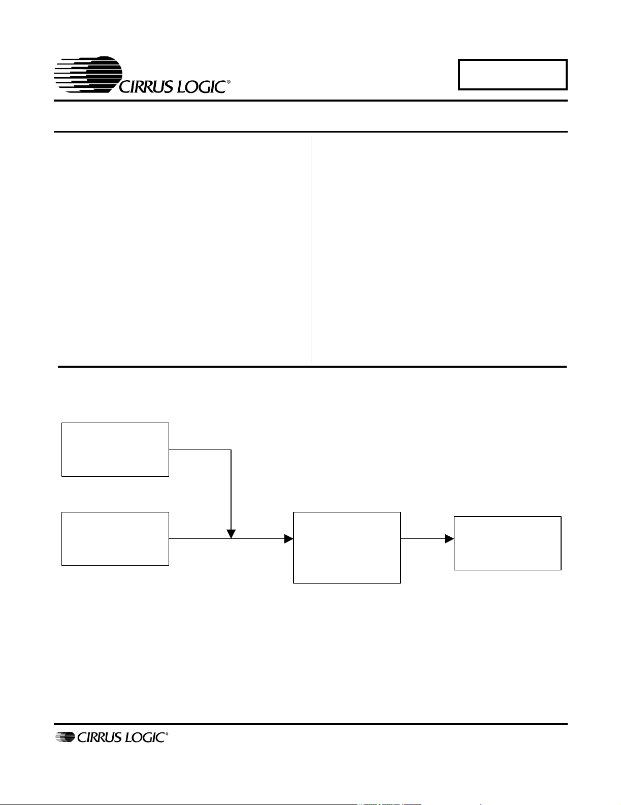
Inputs for Clocks
and Data
CS8416
Digital Audio
Interface
CS4344
Analog Outputs
http://www.cirrus.com
Copyright © Cirrus Logic, Inc. 2004
(All Rights Reserved)
June ‘04
DS613DB2
1
Page 2

TABLE OF CONTENTS
1. CS4344 DIGITAL TO ANALOG CONVERTER . . . . . . . . . . . . . . . . . . . . . . . . . . . . . . . . . . . . 3
2. CS8416 DIGITAL AUDIO RECEIVER . . . . . . . . . . . . . . . . . . . . . . . . . . . . . . . . . . . . . . . . . . . 3
3. INPUT FOR CLOCKS AND DATA . . . . . . . . . . . . . . . . . . . . . . . . . . . . . . . . . . . . . . . . . . . . . . 3
4. POWER SUPPLY CIRCUITRY . . . . . . . . . . . . . . . . . . . . . . . . . . . . . . . . . . . . . . . . . . . . . . . . . 3
5. GROUNDING AND POWER SUPPLY DECOUPLING . . . . . . . . . . . . . . . . . . . . . . . . . . . . . . 4
6. ANALOG OUTPUT FILTERING . . . . . . . . . . . . . . . . . . . . . . . . . . . . . . . . . . . . . . . . . . . . . . . . 4
7. ERRATA . . . . . . . . . . . . . . . . . . . . . . . . . . . . . . . . . . . . . . . . . . . . . . . . . . . . . . . . . . . . . . . . . . 5
LIST OF FIGURES
Figure 1. System Block Diagram and Signal Flow . . . . . . . . . . . . . . . . . . . . . . . . . . . . . . . . . . . 6
Figure 2. CS4344 and outputs . . . . . . . . . . . . . . . . . . . . . . . . . . . . . . . . . . . . . . . . . . . . . . . . . . . 7
CDB4344
Figure 3. CS8416 S/PDIF Input . . . . . . . . . . . . . . . . . . . . . . . . . . . . . . . . . . . . . . . . . . . . . . . . . . . 8
Figure 4. PCM Input Header . . . . . . . . . . . . . . . . . . . . . . . . . . . . . . . . . . . . . . . . . . . . . . . . . . . . . 9
Figure 5. Power Supply Connections . . . . . . . . . . . . . . . . . . . . . . . . . . . . . . . . . . . . . . . . . . . . 10
Figure 6. Silkscreen Top. . . . . . . . . . . . . . . . . . . . . . . . . . . . . . . . . . . . . . . . . . . . . . . . . . . . . . . 11
Figure 7. Top Side . . . . . . . . . . . . . . . . . . . . . . . . . . . . . . . . . . . . . . . . . . . . . . . . . . . . . . . . . . . . 12
Figure 8. Bottom Side . . . . . . . . . . . . . . . . . . . . . . . . . . . . . . . . . . . . . . . . . . . . . . . . . . . . . . . . . 13
2 DS613DB2
Page 3

CDB4344
CDB4344 SYSTEM OVERVIEW
The CDB4344 evaluation board is an excellent means of quickly evaluating the CS4344. The
CS8416 digital audio interface receiver provides an easy interface to digital audio signal sources
including the majority of digital audio test equipment. The evaluation board also allows the user
to supply external PCM clocks and data through a header for system development.
The CDB4344 schematic has been partitioned into 4 schematics shown in Figures 2 through 5.
Each partitioned schematic is represented in the system diagram shown in Figure 1. Notice that
the system diagram also includes the interconnections between the partitioned schematics.
1. CS4344 DIGITAL TO ANALOG CONVERTER
A description of the CS4344 is included in the CS4344 datasheet.
2. CS8416 DIGITAL AUDIO RECEIVER
The system receives and decodes the standard S/PDIF data format using a CS8416 Digital Audio Receiver, Figure 3. The outputs of the CS8416 include a serial bit clock, serial data, left-right
clock, and a 128/256 Fs master clock. The CS8416 data format is fixed to I2S (can be changed
with R42 and R47). The operation of the CS8416 and a discussion of the digital audio interface
is included in the CS8416 datasheet.
The evaluation board has been designed such that the input can be either optical or coax, see
Figure 3. However, both inputs cannot be driven simultaneously.
The right hand switch of S2 sets the output MCLK to LRCK ratio of the CS8416. This switch
should be set to 256 (closed) for inputs Fs<=96 kHz and 128 (open) for Fs>=64 kHz. The 8416
must be manually reset using RX_RST (S1) when this switch is changed.
3. INPUT FOR CLOCKS AND DATA
The evaluation board has been designed to allow interfacing to external systems via the header
J9. Header J9 allows the evaluation board to accept externally generated PCM clocks and data.
The schematic for the clock/data input is shown in Figure 4. The left hand switch of S2 selects
the source as either CS8416 (closed) or header J9 (open).
Please see the CS4344 datasheet for more information.
4. POWER SUPPLY CIRCUITRY
Power is supplied to the evaluation board by three binding posts (GND, +5V, and ‘+3.3V to +5V’),
see Figure 5. The ‘+3.3V to +5V’ which supplies VA can be jumpered to a +3.3 V regulator or the
+5V binding post. The VA supply should be set to the recommended values stated in the CS4344
datasheet.
WARNING: Refer to the CS4344 datasheet for maximum allowable voltages levels. Operation
outside of this range can cause permanent damage to the device.
DS613DB2 3
Page 4
CDB4344
5. GROUNDING AND POWER SUPPLY DECOUPLING
As with any high performance converter, the CS4344 requires careful attention to power supply
and grounding arrangements to optimize performance. Figure 2 details the connections to the
CS4344 and Figures 6, 7, and 8 show the component placement and top and bottom layout. The
decoupling capacitors are located as close to the CS4344 as possible. Extensive use of ground
plane fill in the evaluation board yields large reductions in radiated noise.
6. ANALOG OUTPUT FILTERING
The analog output on the CDB4344 has been designed according to the CS4344 datasheet. This
output circuit includes an AC coupling cap and a single pole R and C. An additional load resistance may be added by stuffing R10 and R26 to test the CS4344’s load driving capability.
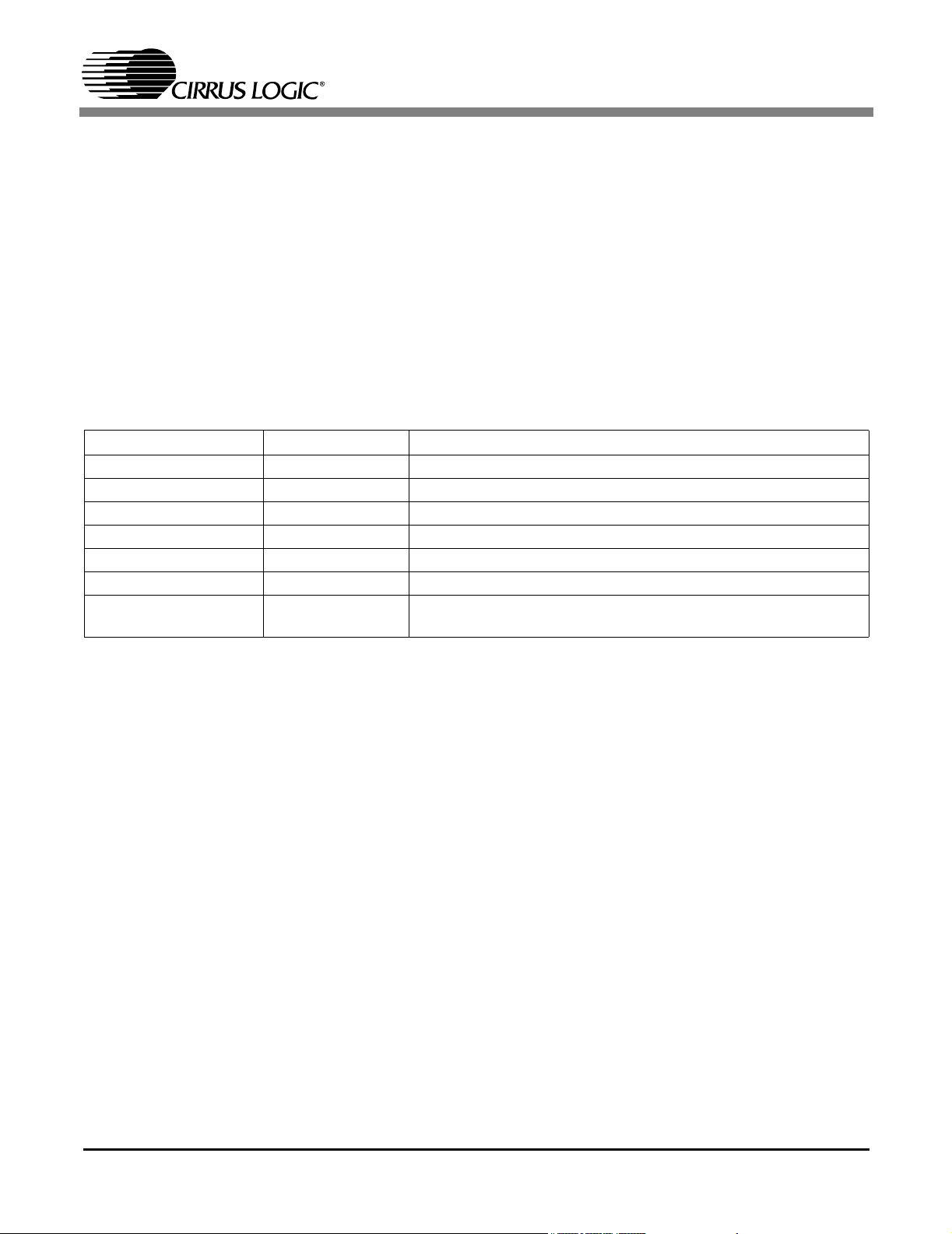
CONNECTOR INPUT/OUTPUT SIGNAL PRESENT
+5V Input + 5 V power
GND Input Ground connection from power supply
+3.3V to +5V Input +3.3 V to +5 V positive supply for the CS4344 VA power
S/PDIF INPUT - J5 Input Digital audio interface input via coax
S/PDIF INPUT - OPT1 Input Digital audio interface input via optical
PCM INPUT - J9 Input Input for master, serial, left/right clocks and serial data
LEFT_OUT and
RIGHT_OUT
Output RCA line level analog outputs
Table 1. System Connections
4 DS613DB2
Page 5
CDB4344
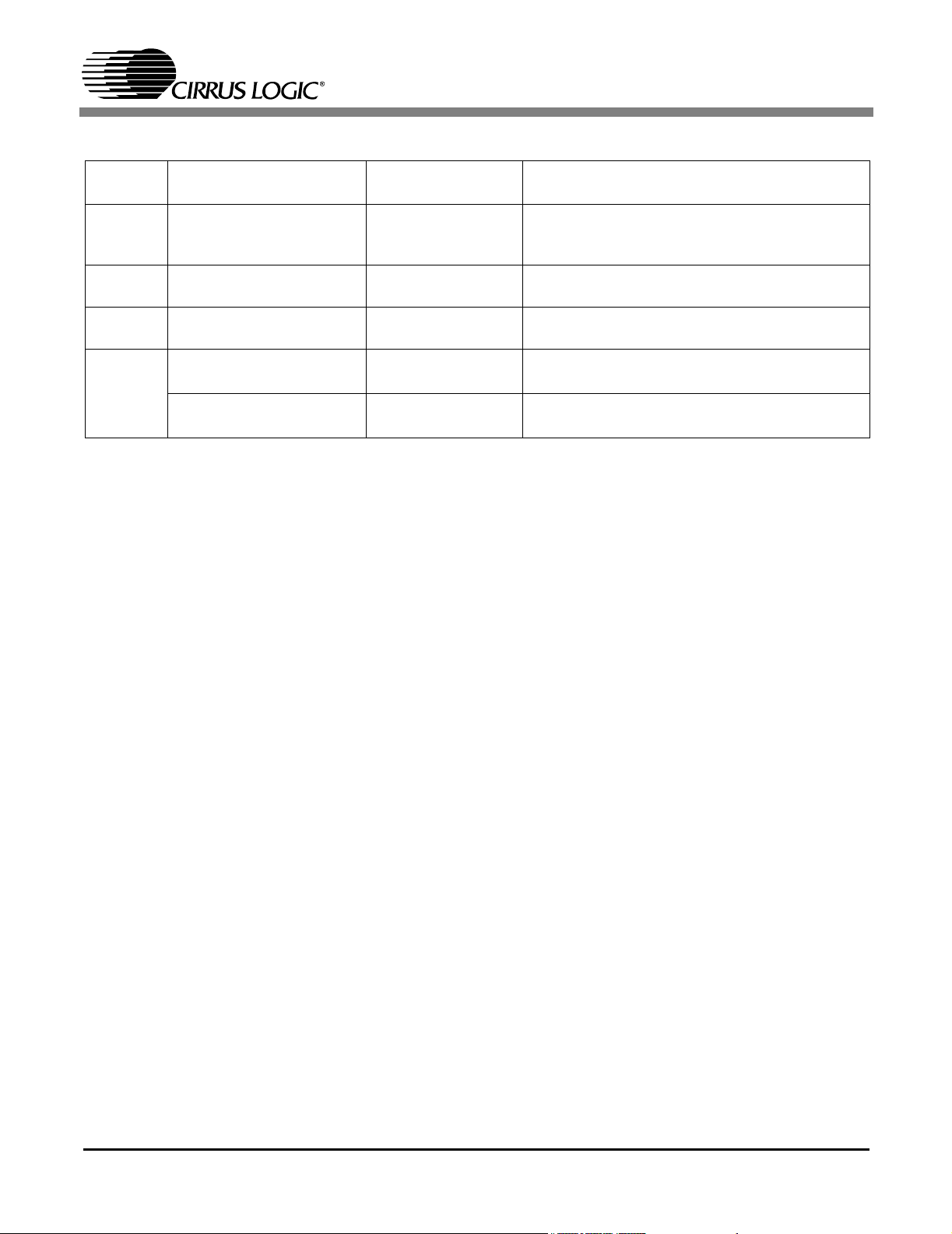
JUMPER /
SWITCH PURPOSE POSITION FUNCTION SELECTED
J4 Selects source of voltage
for the CS4344 VA supply
J7 Provides contact points to
measure current
S1 Resets CS8416 The CS8416 must be reset if switch S2 is
S2 Sets clock source left
Sets MCLK ratio of CS8416 right
Table 2. CDB4344 Jumper Settings
*Default Factory Settings.
VA
+3.3V
*+5V
- Measure voltage across these nodes and divide
Voltage source is the +3.3V to +5V binding post
Voltage source is a +3.3V regulator
Voltage source is +5V binding post
result by 10 to get current in Amps
changed
Sets clock source for CS4344 (open=J9, *closed
= CS8416)
Selects 128x (open) or 256x (*closed)
MCLK/LRCK ratio output for CS8416
7. ERRATA
CDB4344 Revision B.0
Switch S2 is oriented incorrectly on some boards (if open is away from binding posts) and thus
the 0 and 1 labels above and below are incorrect. Using closed for 0 and open for 1, the table
next to the switch will be correct.
DS613DB2 5
Page 6

CDB4344
Figure 5
Power
Left Channel Output
Figure 2
CS4344
Figure 2
Right Channel Output
Figure 2
Figure 1. System Block Diagram and Signal Flow
MCLK
SCLK
LRCK
SDIN
Reset
Circuit
Figure 3
8416 Digital
Audio Receiver
6 DS613DB2
Figure 4
PCM Inputs
Page 7

CDB4344
Figure 2. CS4344 and outputs
DS613DB2 7
Page 8

CDB4344
Figure 3. CS8416 S/PDIF Input
8 DS613DB2
Page 9

CDB4344
Figure 4. PCM Input Header
DS613DB2 9
Page 10

CDB4344
Figure 5. Power Supply Connections
10 DS613DB2
Page 11

CDB4344
Figure 6. Silkscreen Top
DS613DB2 11
Page 12

CDB4344
Figure 7. Top Side
12 DS613DB2
Page 13

CDB4344
Figure 8. Bottom Side
DS613DB2 13
Page 14

CDB4344
REVISION HISTORY
Release Date Changes
DB1 DEC 2003 Initial Release
DB2 JUN 2004 Changed C29 in Figure 2 on page 7 from 3.3 to 10 µF to improve
popguard performance
Contacting Cirrus Logic Support
For all product questions and inquiries contact a Cirrus Logic Sales Representative.
To find one nearest you go to www.cirrus.com
IMPORTANT NOTICE
Cirrus Logic, Inc. and its subsidiaries ("Cirrus") believe that the information contained in this document is accurate and reliable. However, the information is subject to change without notice and is provided "AS IS" without warranty of any kind (express or implied). Customers are advised to obtain the latest version of
relevant information to verify, before placing orders, that information being relied on is current and complete. All products are sold subject to the terms and conditions of sale supplied at the time of order acknowledgment, including those pertaining to warranty, patent infringement, and limitation of liability. No responsibility is assumed by Cirrus for the use of this information, including use of this information as the basis for manufacture or sale of any items, or for infringement
of patents or other rights of third parties. This document is the property of Cirrus and by furnishing this information, Cirrus grants no license, express or implied
under any patents, mask work rights, copyrights, trademarks, trade secrets or other intellectual property rights. Cirrus owns the copyrights associated with the
information contained herein and gives consent for copies to be made of the information only for use within your organization with respect to Cirrus integrated
circuits or other products of Cirrus. This consent does not extend to other copying such as copying for general distribution, advertising or promotional purposes,
or for creating any work for resale.
CERTAIN APPLICATIONS USING SEMICONDUCTOR PRODUCTS MAY INVOLVE POTENTIAL RISKS OF DEATH, PERSONAL INJURY, OR SEVERE
PROPERTY OR ENVIRONMENTAL DAMAGE ("CRITICAL APPLICATIONS"). CIRRUS PRODUCTS ARE NOT DESIGNED, AUTHORIZED OR WARRANTED
FOR USE IN AIRCRAFT SYSTEMS, MILITARY APPLICATIONS, PRODUCTS SURGICALLY IMPLANTED INTO THE BODY, LIFE SUPPORT PRODUCTS
OR OTHER CRITICAL APPLICATIONS (INCLUDING MEDICAL DEVICES, AIRCRAFT SYSTEMS OR COMPONENTS AND PERSONAL OR AUTOMOTIVE
SAFETY OR SECURITY DEVICES). INCLUSION OF CIRRUS PRODUCTS IN SUCH APPLICATIONS IS UNDERSTOOD TO BE FULLY AT THE CUSTOMER'S RISK AND CIRRUS DISCLAIMS AND MAKES NO WARRANTY, EXPRESS, STATUTORY OR IMPLIED, INCLUDING THE IMPLIED WARRANTIES OF
MERCHANTABILITY AND FITNESS FOR PARTICULAR PURPOSE, WITH REGARD TO ANY CIRRUS PRODUCT THAT IS USED IN SUCH A MANNER. IF
THE CUSTOMER OR CUSTOMER'S CUSTOMER USES OR PERMITS THE USE OF CIRRUS PRODUCTS IN CRITICAL APPLICATIONS, CUSTOMER
AGREES, BY SUCH USE, TO FULLY INDEMNIFY CIRRUS, ITS OFFICERS, DIRECTORS, EMPLOYEES, DISTRIBUTORS AND OTHER AGENTS FROM
ANY AND ALL LIABILITY, INCLUDING ATTORNEYS' FEES AND COSTS, THAT MAY RESULT FROM OR ARISE IN CONNECTION WITH THESE USES.
Cirrus Logic, Cirrus, and the Cirrus Logic logo designs are trademarks of Cirrus Logic, Inc. All other brand and product names in this document may be trademarks or service marks of their respective owners.
14 DS613DB2
 Loading...