

Page 1
Evaluation Board for the CS42L73
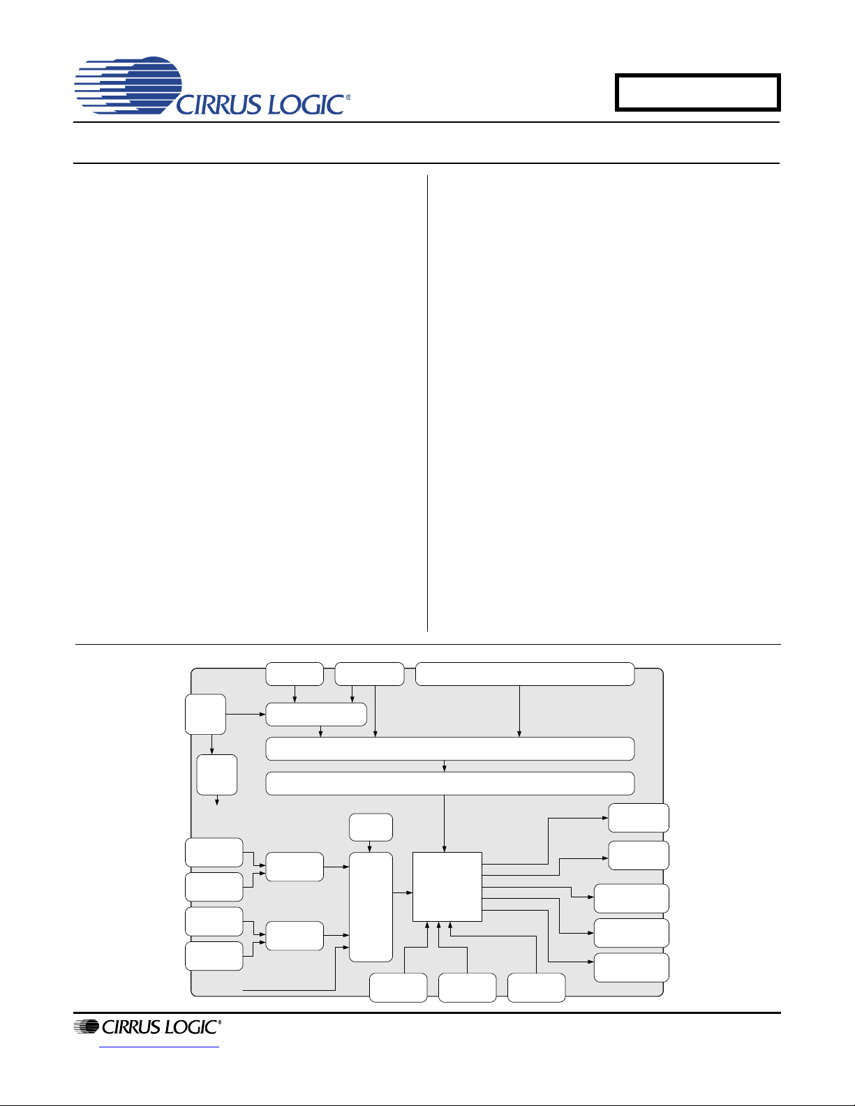
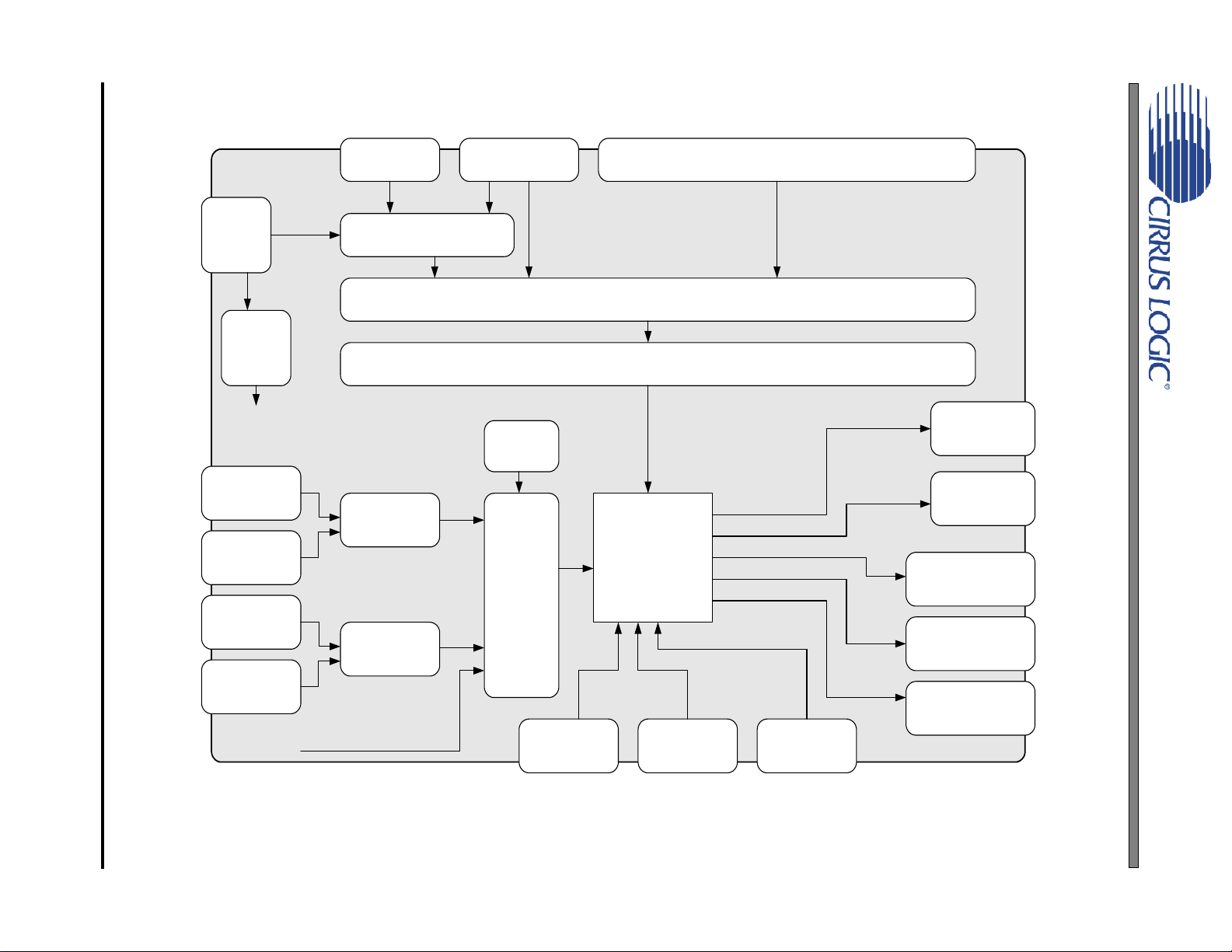
USB
+5V, GND
(Bind. Post)
VA, VP, VCP, VL, VD_FILT
(Bind. Post)
Battery – VP only
(Header)
Regulators
Power Source Selection (Headers)
CS42L73
Current Sense Resistors for Power Measurement (Bypassable)
S/PDIF In
(Optical)
S/PDIF In
(RCA)
S/PDIF Out
(Optical)
S/PDIF In
(RCA)
CS8416
CS8406
Clocks
And
Data
Selection
(Headers)
Micro-
Controller
Canned
Oscillator
I2C and Board
Controls
Line In Stereo
(RCA)
Mic In 1 and 2
(1/8")
Digital Mic In
(Header)
Headphone Out
(1/8")
Lineout Stereo
(RCA)
Spkphone Out
(Term. Block & 1/8")
Spkphone/Line Out
(Term. Block & 1/8")
Earphone Out
(Term. Block & 1/8")
Direct External Digital
I/O
CDB42L73
Features
Analog Inputs
– Line-level In via 2x mono RCA jacks
– Microphone In via 2x mono 1/8” jacks
Analog outputs
– Headphone out via 1x stereo 1/8” jack
– Line-level out via 2x mono RCA jacks
– Earphone out via terminal block
– Speakerphone out via terminal blocks
S/PDIF interface via RCA/optical jacks
– Input: CS8416 digital audio receiver
– Output: CS8406 digital audio transmitter
External digital I/O via stake headers
– Digital mic in
– Serial audio port I/O
– External I²C
Flexible power-supply configuration
– USB, external power supply, or battery
FlexGUI software control
– Windows® compatible
– Predefined and user-configurable scripts
™
control port I/O
Description
The CDB42L73 board is a dedicated platform for testing
and evaluating the CS42L73, an ultralow power mobile
audio and telephony CODEC.
To allow comprehensive testing of CS42L73 features
and performance, extensive hardware and software
configurable options are available on the CDB42L73.
Hardware options, such as power-supply settings, are
configured via jumpers on the stake headers.
Software options, such as registry settings for the
CS42L73, are configured with the FlexGUI software,
which communicates with the CDB42L73 via USB from
a Windows
I/O headers on the CDB42L73 allow external control
signals (for example, an external DSP or microcontroller) to configure and interface with the CS42L73 and
other devices directly without the use of FlexGUI.
The CDB42L73 also serves as a good component and
layout reference for the CS42L73.
ORDERING INFORMATION
CDB42L73 Evaluation Board
®
compatible computer. In addition, digital
http://www.cirrus.com
Copyright Cirrus Logic, Inc. 2010
(All Rights Reserved)
JUNE '10
DS882DB1
Page 2

TABLE OF CONTENTS
1. QUICK SETUP GUIDE ........................................................................................................................... 4
2. THE CDB42L73 SYSTEM OVERVIEW .................................................................................................. 5
2.1 Power Supply Circuitry ..................................................................................................................... 5
2.2 Digital Inputs and Outputs ................................................................................................................ 5
2.3 Digital Mic Input ................................................................................................................................ 5
2.4 Analog Inputs .................................................................................................................................... 6
2.5 Analog Outputs ................................................................................................................................. 6
2.6 Control Port Interface ....................................................................................................................... 6
2.7 Layout Reference ............................................................................................................................. 6
2.8 CS42L73 Ultralow Power Mobile Audio and Telephony CODEC ..................................................... 7
2.9 Performance Measurement Tips ...................................................................................................... 7
3. SYSTEM CONNECTIONS AND JUMPER SETTINGS .......................................................................... 8
4. SOFTWARE CONTROL USING FLEXGUI .......................................................................................... 12
4.1 Installation and First-time Setup ..................................................................................................... 12
4.2 Working with Register Settings ....................................................................................................... 12
4.2.1 Modifying Register Settings Manually ................................................................................... 12
4.2.2 Save or Restore Register Settings ........................................................................................12
4.3 Using the FlexGUI High-level Interface Layout ..............................................................................13
4.3.1 S/PDIF Tab ............................................................................................................................ 14
4.3.2 Power Tab ............................................................................................................................. 15
4.3.3 Clocking XSP VSP ASP Tab .................................................................................................16
4.3.4 Analog Input Tab ................................................................................................................... 17
4.3.5 Input DSP Tab ....................................................................................................................... 18
4.3.6 Digital Mixer 1 Tab ................................................................................................................ 19
4.3.7 Digital Mixer 2 Tab ................................................................................................................ 20
4.3.8 Output DSP Tab .................................................................................................................... 21
4.3.9 Analog Output Tab ................................................................................................................ 22
4.4 The Register Map ........................................................................................................................... 23
5. SCHEMATICS AND LAYOUT ........................................................................................................ 24
6. REVISION HISTORY ........................................................................................................................... 36
CDB42L73
LIST OF FIGURES
Figure 1. CDB42L73 Factory Default Jumper Settings .............................................................................11
Figure 2. Save Register Settings .............................................................................................................. 12
Figure 3. Restore Register Settings .......................................................................................................... 12
Figure 4. FlexGUI Tabs ............................................................................................................................. 13
Figure 5. Correlating the FlexGUI Tabs to the Audio Signal Chain ........................................................... 13
Figure 6. The “S/PDIF” Tab in FlexGUI for the CDB42L73 ....................................................................... 14
Figure 7. The “Power” Tab in FlexGUI for the CDB42L73 ........................................................................ 15
Figure 8. The “Clocking XSP VSP ASP” Tab in FlexGUI for the CDB42L73 ............................................ 16
Figure 9. The “Analog Input” Tab in FlexGUI for the CDB42L73 .............................................................. 17
Figure 10. The “Input DSP” Tab in FlexGUI for the CDB42L73 ................................................................ 18
Figure 11. The “Digital Mixer 1” Tab in FlexGUI for the CDB42L73 .......................................................... 19
Figure 12. The “Digital Mixer 2” Tab in FlexGUI for the CDB42L73 .......................................................... 20
Figure 13. The “Output DSP” Tab in FlexGUI for the CDB42L73 ............................................................. 21
Figure 14. The “Analog Output” Tab in FlexGUI for the CDB42L73 ......................................................... 22
Figure 15. The “Register Maps” Tab in FlexGUI for the CDB42L73 ......................................................... 23
Figure 16. System Block Diagram ............................................................................................................. 24
Figure 17. CS42L73 .................................................................................................................................. 25
Figure 18. USB and Microcontroller .......................................................................................................... 26
Figure 19. S/PDIF Receiver and Transmitter; Clock Buffers ..................................................................... 27
2 DS882DB1
Page 3

Figure 20. Power ....................................................................................................................................... 28
Figure 21. Top Side Silkscreen ................................................................................................................. 29
Figure 22. Layer 1 ..................................................................................................................................... 30
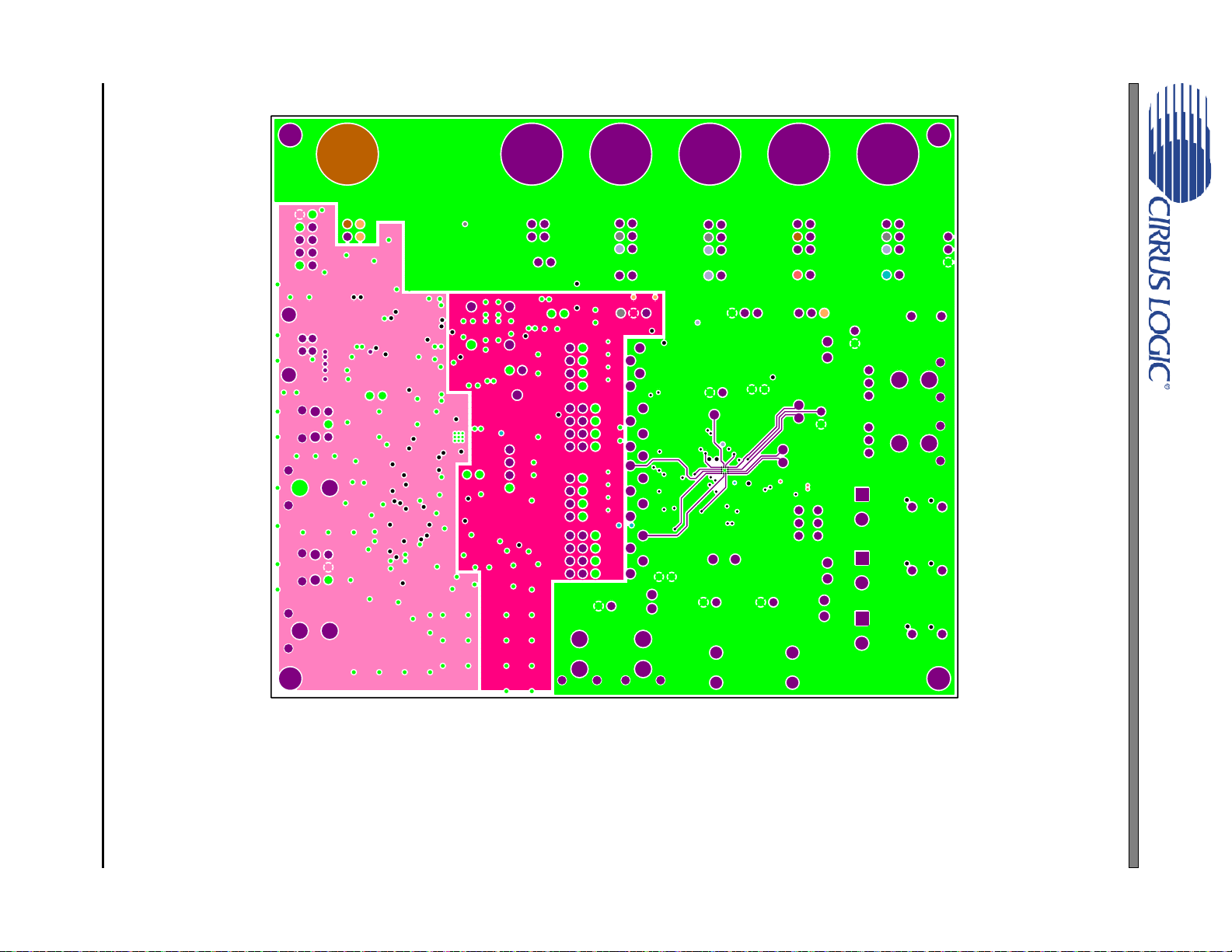
Figure 23. Layer 2 ..................................................................................................................................... 31
Figure 24. Layer 3 ..................................................................................................................................... 32
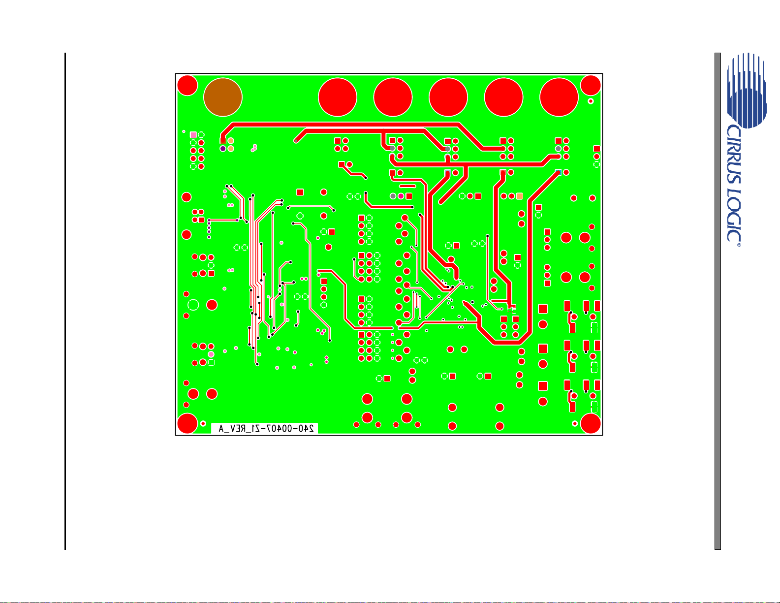
Figure 25. Layer 4 ..................................................................................................................................... 33
Figure 26. Layer 5 ..................................................................................................................................... 34
Figure 27. Layer 6 ..................................................................................................................................... 35
LIST OF TABLES
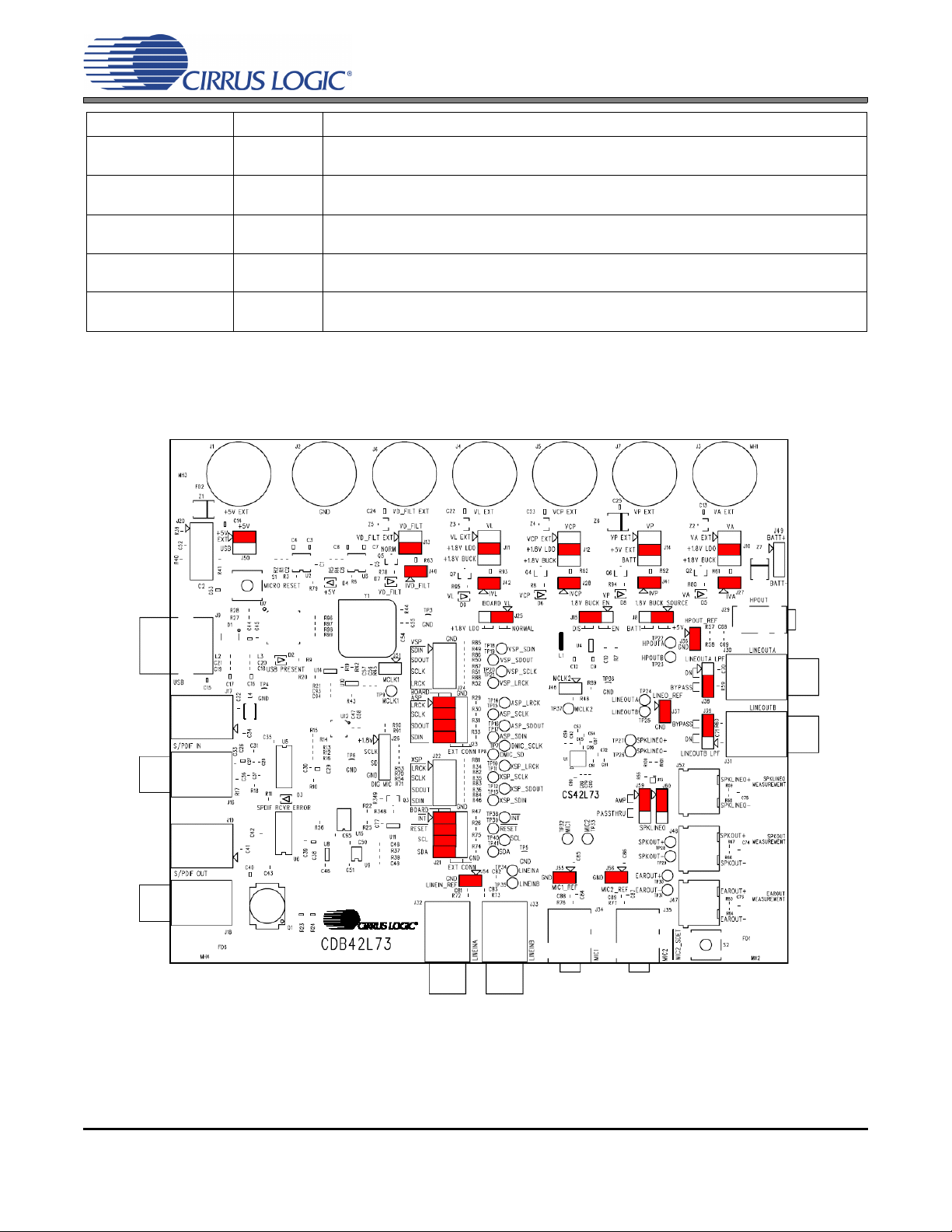
Table 1. System Connections .................................................................................................................... 8
Table 2. CDB42L73 Jumper Settings ........................................................................................................ 10
Table 3. LED Information .......................................................................................................................... 11
CDB42L73
DS882DB1 3
Page 4

CDB42L73
1. QUICK SETUP GUIDE
This section describes a short procedure to set the CDB42L73 to a standard state for evaluation.
1. Return all jumpers to their factory default settings as described in Table 2 on page 10, and displayed in Fig-
ure 1 on page 11
2. Install the FlexGUI software as outlined in Section 4.2 on page 12.
3. Connect a +5 V power supply to the +5 V Ext (J1) and GND (J2) binding post on the CDB42L73.
4. Connect a USB cable from a Windows
5. Run the FlexGUI software. Restore one of the two factory pre-configured signal test paths (read more about
restoring settings in Section 4.2.2 on page 12):
• Line input to Audio Serial Port output; Audio Serial Port input to headphone/line output
Restore register file: “Factory_Default_LINEIN_to_ASPOUT_ASPIN_to HP_LINEOUT.fgs”
The line inputs are labeled J32 and J33; the headphone output is J29; the line outputs J30 and J31. Audio Serial Port input/outputs are connected via the S/PDIF connectors J16 through J19.
• Microphone input to Audio Serial Port output; Audio Serial Port input to speakerphone/earphone output
Restore register file: “Factory_Default_MICIN_to_ASPOUT_ASPIN_to_SPKrs.fgs”
The microphone inputs are labeled J34 and J35; the speakerphone output is J48; the earphone output
is J47. Audio Serial Port input/outputs are connected via the S/PDIF connectors J16 through J19.
®
-compatible PC to the CDB42L73.
4 DS882DB1
Page 5

CDB42L73
2. THE CDB42L73 SYSTEM OVERVIEW
The CDB42L73 evaluation board is a convenient platform for evaluating the CS42L73 ultralow-power mobile and
telephony CODEC. It supports multiple power supply and signal I/O configurations, including the option to drive the
CS42L73 externally (which bypasses on-board circuitry). The CDB42L73 is also a good component and layout reference for the CS42L73.
Section 2.1 through Section 2.8 below describe the various features of the CDB42L73 evaluation board in detail.
Section 2.9 lists several useful performance measurement tips when evaluating the CDB42L73.
2.1 Power Supply Circuitry
The CDB42L73 is designed to be powered by a single +5 V DC power supply. This can be provided by an
external +5 V power supply unit or a regular USB connection, selectable via jumper pin block J50. If using
a USB connection to supply power, the VP supply pin of the CS42L73 requires an external source (J7 or
J49); this is due to the high power requirements of driving a speakerphone. At full speakerphone volume,
the current consumption of the VP supply pin may exceed the current supply capabilities of a typical USB
connection.
Low-dropout regulators (LDOs) step down the +5 V supply to provide clean and stable 3.3 V and 1.8 V rails
to all the onboard circuitry and the CS42L73.
There is also a switching buck regulator which may be used to supply a 1.8 V rail. The buck regulator’s
source, either the main +5 V supply or an external battery, is selectable via jumper pin block J8. It is enabled/disabled with J15. The external battery connection is J49.
Jumper pin blocks J10, J11, J12, J13, and J14 select the power supply source for the CS42L73 supply pins.
In most cases, the selections are between an external supply, the LDO-derived 1.8 V, or the buck-derived
1.8 V.
Jumper pin block J25 selects the source of the CS42L73’s interface voltage, VL. When J25 is shunted in
the “NORM” position, all devices on the board (including the CS42L73) share the same VL supply as selected on J11. However, in strict battery life testing of the CS42L73, it may be useful to decouple the power
usage of VL of peripheral devices (such as signal level shifters) from that of the CS42L73. When J25 is
shunted In the “+1.8V LDO” position, VL for peripheral devices on the CDB42L73 is sourced from the +1.8 V
LDO, while VL for the CS42L73 is determined by the selection on J11.
2.2 Digital Inputs and Outputs
The S/PDIF interface on the CDB42L73 accepts coaxial or optical connections for both inputs and outputs.
S/PDIF inputs are handled by the CS8416 receiver; S/PDIF outputs by the CS8406 transmitter. On the
CDB42L73, the CS8416 is configured to operate only in master mode, while the CS8406 is to work only in
slave mode.
Please note that the S/PDIF interface is routed only to the Audio Serial Port (ASP) of the CS42L73; however,
the ASP may also be driven externally via header J23. The Voice Serial Port (VSP) and Auxiliary Serial Port
(XSP) may only be driven externally via headers J24 and J22, respectively.
A complete description of the CS8416 S/PDIF receiver and CS8406 S/PDIF transmitter can be found in their
respective datasheets, downloadable from http://www.cirrus.com.
2.3 Digital Mic Input
The digital mic input header, J26, allows up to two digital microphones to interface with the CS42L73. A ribbon cable is required to connect the digital microphones to J26.
DS882DB1 5
Page 6

2.4 Analog Inputs
Line input (via 2x mono RCA jacks) and microphone input (via 2x mono 1/8-inch jacks) are available on the
CDB42L73. Analog input circuitry simply consists of DC-blocking capacitors and several resistors as shown
in the Typical Connections Diagram of the CS42L73 datasheet.
Button switch S2 engages the CS42L73’s MIC2 automute function when pressed.
Jumper pin blocks J54, J55, and J56 allow the user to evaluate the pseudo-differential analog input features
of the CS42L73. By default, shunts are placed on these jumper pin blocks to emulate a typical single-ended
input use case. When the shunts are removed, the pseudo-differential analog inputs will reject commonmode noise effectively; this is especially useful for eliminating ground loop related problems from the analog
input source.
2.5 Analog Outputs
Line output (via 2x mono RCA jacks) and headphone output (via 1x stereo 1/8-inch jack) are available on
the CDB42L73. The line output also has a selectable first order low-pass filter commonly used with DACs;
this is done via jumper pin blocks J38 and J39. In addition, jumper pin blocks J36 and J37 allow the user to
evaluate the pseudo-differential line/headphone output capability of the CS42L73. By default, J36 and J37
are shunted to emulate a typical single-ended output use case. When the shunts are removed, the pseudodifferential line/headphone outputs will reject common-mode noise effectively; this is especially useful for
eliminating ground loop related problems arising from an external connection to the line/headphone outputs.
CDB42L73
The differential earphone, speakerphone, and speakerphone line outputs are provided via terminal blocks
J47, J48, and J52. Each of these outputs has a 1/8-inch jack in parallel to be used as the measurement
point when test loads are connected to the terminal blocks.
It should be noted that the CS35L01 Class-D amplifier (reference designator U13) may be used to amplify
the speakerphone line output. The CS35L01-amplified speakerphone line output may be selected by shunting jumper pin blocks J59 and J60 to the “AMP” position. This is useful when trying to achieve a stereo
speaker driver configuration; for example, the speakerphone output of the CS42L73 may be used as the left
speaker driver, while the amplified speakerphone line output may be used as the right speaker driver. The
CS35L01 may be enabled or disabled via FlexGUI by toggling bit 7 of address 0x01 in the “Micro” tab of the
Register Maps.
2.6 Control Port Interface
The Cirrus Logic FlexGUI software application (downloadable from http://www.cirrus.com/msasoftware)
provides users an easy and intuitive way to configure the CDB42L73. A Windows
connectivity is required to run FlexGUI.
The CDB42L73’s onboard microcontroller handles the USB communication with FlexGUI and the control
port interface of the CS42L73. The control port interface of the CS42L73 is routed through jumper pin block
J21. When the pin columns marked “BOARD” are shunted (the default setting), the microcontroller handles
all communication between the FlexGUI application and the CS42L73. If external control is to be used instead of FlexGUI, the shunts on J21 should be removed and the external signals wired in to the pin columns
marked “EXT CONN” (please note the GND pins on the right hand side).
®
-compatible PC with USB
2.7 Layout Reference
The CDB42L73 utilizes a six-layer PCB that allows for clean trace fanout from the CS42L73. There are also
dedicated ground planes between each routed layer, providing low-impedance return paths for high frequency signals and improving shielding between layers. Local decoupling and fly capacitors for the
CS42L73 are placed as closely as possible to the device, with the critical components closest.
6 DS882DB1
Page 7

2.8 CS42L73 Ultralow Power Mobile Audio and Telephony CODEC
The CS42L73 is a highly integrated, ultralow power, audio and telephony CODEC for portable applications.
It features microphone and line inputs; three bidirectional serial ports with high-performance ASRCs; and
headphone, line, and speaker amplifiers. A complete description of the CS42L73 can be found in its
datasheet, downloadable from http://www.cirrus.com.
2.9 Performance Measurement Tips
• Low frequency THD+N and common mode rejection performance may be improved by increasing the
capacitance of the DC-blocking capacitors on the line and microphone inputs (C81, C82, C83, C84, C85,
C86, C87).
• Interchannel isolation (crosstalk) performance of the CS42L73’s headphone output should be measured
with headphone loads connected between TP22 and GND (TP36), and between TP23 and GND (TP36).
These connection points provide the lowest impedance return paths for the headphone loads to reflect
the full headphone crosstalk performance of the CS42L73.
• Dynamic range and THD+N measurement of the CS35L01 (when J59 and J60 are shunted to the “AMP”
position) should be made with an external filter such as the AP AUX-0025 Switching Amplifier Measurement Filter. Filters such as the AUX-0025 prevent switching noise of Class-D amplifiers from affecting
measurement accuracy of traditional audio analyzers.
CDB42L73
DS882DB1 7
Page 8
CDB42L73
3. SYSTEM CONNECTIONS AND JUMPER SETTINGS
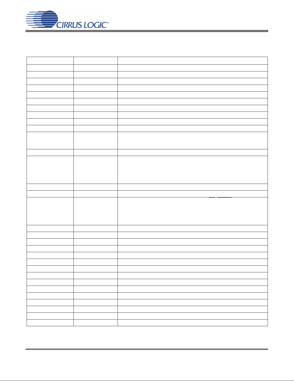
Board connections and settings are shown in Table 1 and Table 2 below.
CONNECTOR INPUT/OUTPUT CONNECTION TYPE AND SIGNAL IF PRESENT
J1 +5V EXT Input +5V external power supply
J2 GND Input Evaluation board ground
J3 VA EXT Input CS42L73 VA external supply
J4 VL EXT Input CS42L73 VL external supply
J5 VCP EXT Input CS42L73 VCP external supply
J6 VD_FILT EXT Input CS42L73 VD_FILT external supply
J7 VP EXT Input CS42L73 VP external supply
J20 C2 Input Microcontroller programming header
J9 USB Input/Output USB connection
J49 BATT Input External battery header
J51 MCLK1 Input CS42L73 MCLK1 external master clock connection
- By default, Y1 oscillator is populated and used for MCLK1.
- Remove Y1 oscillator before connecting external master clock.
J46 MCLK2 Input CS42L73 MCLK2 external master clock connection
J23 ASP Input/Output CS42L73 Audio Serial Port (LRCK, SCLK, SDIN, SDOUT)
- By default, shunts connect the columns marked “BOARD.” This connects the
CS42L73 Audio Serial port to the S/PDIF interface.
- To use external clock and data signals, remove shunts. Connect external signal and ground to columns marked “EXT CONN.”
J24 VSP Input/Output CS42L73 Voice Serial Port (LRCK, SCLK, SDIN, SDOUT)
J22 XSP Input/Output CS42L73 Auxiliary Serial Port (LRCK, SCLK, SDIN, SDOUT)
J21 Input/Output CS42L73 control port connections (SDA, SCL, INT
- By default, shunts connect the columns marked “BOARD.” This connects the
microcontroller to the control port of the CS42L73.
- To use external control signals, remove shunts. Connect external signal and
ground to columns marked “EXT CONN.”
J26 DIG MIC Input CS42L73 Digital microphone connection (SCLK, SD, GND, +1.8 V supply)
J16 S/PDIF IN Input Coaxial S/PDIF digital input
J17 S/PDIF IN Input Optical S/PDIF digital input
J18 S/PDIF OUT Output Coaxial S/PDIF digital output
J19 S/PDIF OUT Output Optical S/PDIF digital output
J32 LINEINA Input CS42L73 line input channel A
J33 LINEINB Input CS42L73 line input channel B
J34 MIC1 Input CS42L73 microphone input channel A
J35 MIC2 Input CS42L73 microphone input channel B
J29 HPOUT Output CS42L73 headphone output channel A and B
J30 LINEOUTA Output CS42L73 line output channel A
J31 LINEOUTB Output CS42L73 line output channel B
J52 SPKLINEO Output CS42L73 speakerphone line output
J48 SPKOUT Output CS42L73 speakerphone output
J47 EAROUT Output CS42L73 earphone output
Table 1. System Connections
, RESET)
8 DS882DB1
Page 9
CDB42L73
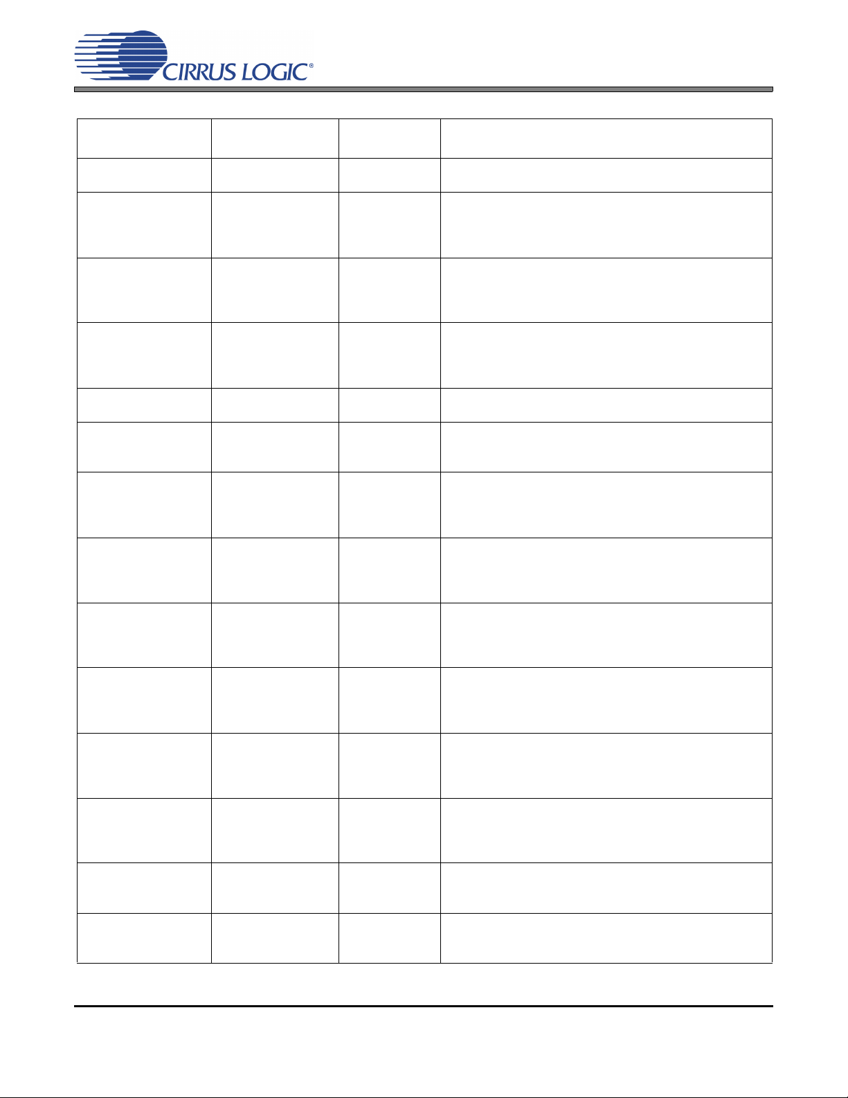
JUMPER PIN
BLOCK
J50 +5 V +5 V main supply
J10 VA CS42L73 VA supply
J11 VL CDB42L73 VL supply
J12 VCP CS42L73 VCP sup-
J13 VD_FILT CS42L73 VD_FILT
J14 VP CS42L73 VP supply
J25 BOARD VL CDB42L73 board
J27 IVA CS42L73 VA current
J42 IVL CS42L73 VL current
J28 IVCP CS42L73 VCP cur-
J40 IVD_FILT CS42L73 current
J41 IVP CS42L73 current
J15 1.8V BUCK EN +1.8 V switching buck
J8 1.8V BUCK
SOURCE
PURPOSE POSITION FUNCTION SELECTED
select
source select
source select
(see also J25)
ply source select
supply source select
source select
peripheral and
CS42L73 VL common
supply toggle
measurement
measurement
rent measurement
measurement
measurement
regulator enable/dis-
able
+1.8 V switching buck
regulator power sup-
ply source
[*] +5V EXT
VA E X T
[*] +1.8 V LDO
+1.8 V BUCK
VL EXT
[*] +1.8 V LDO
+1.8 V BUCK
VCP EXT
[*] +1.8 V LDO
+1.8 V BUCK
VD_FILT_EXT
[*] NORM
VP EXT
[*] +5 V EXT
+1.8 V LDO
[*] NORMAL
[*] Shunted
[*] Shunted
[*] Shunted
[*] Shunted
[*] Shunted
[*] DISENDisables the +1.8 V switching buck regulator
[*] +5V
+5 V supply source from J1
USB
+5 V supply source from USB
CS42L73 VA supply = J3
CS42L73 VA supply= 1.8 V derived from LDO
CS42L73 VA supply= 1.8 V derived from switching buck
regulator
CDB42L73 VL supply = J4
CDB42L73 VL supply = 1.8 V derived from LDO
CDB42L73 VL supply = 1.8 V derived from switching buck
regulator
CS42L73 VCP supply = J5
CS42L73 VCP supply = 1.8 V derived from LDO
CS42L73 VCP supply = 1.8 V derived from switching buck
regulator
CS42L73 digital core supply = J6
CS42L73 digital core supply = internally generated
CS42L73 VP supply = J7
CS42L73 VP supply = J1
BATT
CS42L73 VP supply = J49
Board peripheral VL is supplied by 1.8 V LDO while
CS42L73 VL = J11
Board peripheral VL and CS42L73 VL = J11
0.1 current measurement resistor is shorted
Open
0.1 current measurement resistor is in series with
CS42L73 VA, allowing user to measure current draw of VA
supply for power consumption calculations.
0.1 current measurement resistor is shorted
Open
0.1 current measurement resistor is in series with
CS42L73 VL, allowing user to measure current draw of VL
supply for power consumption calculations.
0.1 current measurement resistor is shorted
Open
0.1 current measurement resistor is in series with
CS42L73 VCP, allowing user to measure current draw of
VCP supply for power consumption calculations.
0.1 current measurement resistor is shorted
Open
0.1 current measurement resistor is in series with
CS42L73 VD_FILT, allowing user to measure current draw
of digital core supply for power consumption calculations.
0.1 current measurement resistor is shorted
Open
0.1 current measurement resistor is in series with
CS42L73 VP, allowing user to measure current draw of VP
supply for power consumption calculations.
Enables the +1.8 V switching buck regulator
BATT
+1.8V switching buck regulator power supply source = J49
+1.8V switching buck regulator power supply source = J50
DS882DB1 9
Page 10
CDB42L73
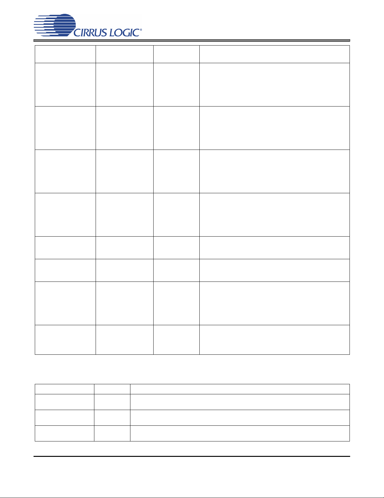
JUMPER PIN
BLOCK
J54 LINEIN_REF Line input reference
J55 MIC1_REF MIC1 reference to
J56 MIC2_REF MIC2 reference to
J36 HPOUT_REF Headphone output
J38 LINEOUTA LPF Line output A low-
J39 LINEOUTB LPF Line output B low-
J37 LINEO_REF Line output reference
J59, J60 SPKLINEO Speakerphone line
PURPOSE POSITION FUNCTION SELECTED
to GND select
GND select
GND select
reference to GND
select
pass filter enable/dis-
able
pass filter enable/dis-
able
to GND select
output to CS35L01 or
passthrough
[*] Shunted
[*] Shunted
[*] Shunted
[*] Shunted
[*] BYPASSONLine output A low-pass filter is disabled
[*] BYPASSONLine output B low-pass filter is disabled
[*] Shunted
[*] AMP
PASSTHRU
Line input shield connection of J32 and J33 is shunted to
board ground.
Open
Line input shield connection of J32 and J33 is not connected to board ground, thus the CS42L73 line input is referenced to the incoming signal reference instead of the
board ground.
MIC1 input shield connection of J34 is shunted to board
ground.
Open
MIC1 input shield connection of J34 is not connected to
board ground, thus the CS42L73 MIC1 input is referenced
to the incoming signal reference instead of the board
ground.
MIC2 input shield connection of J35 is shunted to board
ground.
Open
MIC2 input shield connection of J35 is not connected to
board ground, thus the CS42L73 MIC2 input is referenced
to the incoming signal reference instead of the board
ground.
Headphone output shield connection of J29 is shunted to
board ground.
Open
Headphone output shield connection of J29 is not connected to board ground, thus the CS42L73 headphone output is referenced to the outgoing connection reference
instead of the board ground.
Line output A low-pass filter is enabled
Line output B low-pass filter is enabled
Line output shield connection of J30 and J31 is shunted to
board ground.
Open
Line output shield connection of J30 and J31 is not connected to board ground, thus the CS42L73 headphone output is referenced to the outgoing connection reference
instead of the board ground.
Output on J48 is amplified by the CS35L01 class-D amplifier.
Output on J48 is direct connected to the CS42L73 speakerphone line output pins.
Table 2. CDB42L73 Jumper Settings
LED STATUS FUNCTION
D2 USB PRESENT On
Off
D3 SPDIF ERROR On
Off
D4 +5V On
Off
Indicates there is a USB connection to the CDB42L73.
Indicates there is not a USB connection to the CDB42L73.
Indicates there is either no S/PDIF input or error in the S/PDIF data stream.
Indicates the connected S/PDIF input is valid.
Indicates the +5 V main supply is powered.
Indicates the +5 V main supply is not powered.
10 DS882DB1
Page 11
LED STATUS FUNCTION
Figure 1. CDB42L73 Factory Default Jumper Settings
D5 VA On
Off
D6 VCP On
Off
D7 VD_FILT On
Off
D8 VP On
Off
D9( VL On
Off
Indicates the CS42L73 VA supply is powered.
Indicates the CS42L73 VA supply is not powered.
Indicates the CS42L73 VCP supply is powered.
Indicates the CS42L73 VCP supply is not powered.
Indicates the CS42L73 VD_FILT supply is powered.
Indicates the CS42L73 VD_FILT supply is not powered.
Indicates the CS42L73 VP supply is powered.
Indicates the CS42L73 VP supply is not powered.
Indicates the CS42L73 VL supply is powered.
Indicates the CS42L73 VL supply is not powered.
Table 3. LED Information
Note: All settings denoted by the symbol [*] are the Default Factory Settings.
CDB42L73
DS882DB1 11
Page 12

4. SOFTWARE CONTROL USING FLEXGUI
Figure 2. Save Register Settings Figure 3. Restore Register Settings
4.1 Installation and First-time Setup
The Cirrus Logic FlexGUI application is a graphical user interface that allows users to easily configure software modifiable options on the CDB42L73, such as the register settings of the CS42L73 and the S/PDIF
interface devices (CS8416, CS8406).
To set up FlexGUI for use with the CDB42L73, please follow these steps:
1. Download the latest version of the FlexGUI control software from www.cirrus.com/msasoftware. Follow
the installation instructions on the download page.
2. Connect the CDB42L73 to the host PC using a USB cable.
3. Launch FlexGUI. Note: Once the GUI is launched successfully, all registers are set to their default reset
state.
Note: To start evaluating the CS42L73 immediately with several standard configurations used at the fac-
tory, load the predefined register settings as described in Section 4.2.2 Save or Restore Register
Settings for instructions.
4.2 Working with Register Settings
4.2.1 Modifying Register Settings Manually
CDB42L73
Once FlexGUI is up and running, there are two ways to modify register settings manually:
• Use the high-level interface, which features intuitive GUI elements such as sliders, check boxes, and
drop-down menus. Please see Section 4.3 Using the FlexGUI High-level Interface Layout for more details on using the high-level interface.
• Use the low-level register map, which displays the entire user configurable register space for each device on the CDB42L73 in table form. Register changes may be done on a per-bit or per-address basis.
Please see Section 4.4 The Register Map on page 23 for more details on the register map.
4.2.2 Save or Restore Register Settings
FlexGUI also allows saving the current state of all register settings to a file, which can be easily restored
later.
To save the current register settings, click on the File menu, then click “Save Board Registers” (Figure 2).
Enter a suitable file name and click “Save.”
To restore pre-defined/saved register settings, click on the File menu, then click “Restore Board Registers” (Figure 3). Choose the desired register setting and click “Open.”
12 DS882DB1
Page 13

To restore one of several standard configurations pre-defined at the factory, load the register settings
Figure 4. FlexGUI Tabs
Anlg Input Input DSP
Dig Mixer 1
&
Dig Mixer 2
Output
DSP
Anlg Output
Clocking XSP VSP ASP
A/D
Digital In
Digital Out
Digital
Analog Signal
(Mic In, Line In)
Digital D/A
Analog Signal
(HP Out, Line Out,
Spk Out, Spkline Out,
Ear Out)
Legend:
Represents a tab/page
in the GUI
Shows the direction
of the audio signal
S/PDIF
Aux Serial Port
(ASP)
Video Serial Port
(ASP)
Audio Serial Port
(ASP)
S/PDIF
Input and
Output
Figure 5. Correlating the FlexGUI Tabs to the Audio Signal Chain
starting with “Factory_Default” in its file name. The file names are meant to be self-explanatory. For example, if “Factory_Default_LINEIN_to_ASPOUT_ASPIN_to HP_LINEOUT.fgs” is loaded, the Line Input
is routed to the Audio Serial Port to the S/PDIF output, and the S/PDIF input is routed to the Audio Serial
Port to the Headphone and Line Output.
4.3 Using the FlexGUI High-level Interface Layout
The CS42L73 is a versatile CODEC with many features and register settings. To keep the GUI easy to use
and visually clean, register controls for the CS42L73 are grouped by function and their location in the signal
chain. The result is a series of tabs arranged to mirror the CS42L73’s major functional blocks as closely as
possible (the S/PDIF tab is an exception in that it is not part of the CS42L73 but its functionality in the system
is important enough to warrant a tab in the GUI).
Figure 4 below shows the tabs in the FlexGUI high-level interface layout.
CDB42L73
Figure 5 below is a flow diagram to help users map the FlexGUI tabs to their respective function in the audio
signal chain.
The subsequent sections, Section 4.3.1 through Section 4.3.9, describe each tab in detail.
DS882DB1 13
Page 14

4.3.1 S/PDIF Tab
Figure 6. The “S/PDIF” Tab in FlexGUI for the CDB42L73
The “S/PDIF” tab contains the main controls for setting up the S/PDIF interface of the CDB42L73. A brief
description of each control group is described below.
• S/PDIF Receiver (CS8416) - register controls for configuring the CS8416 to accommodate the S/PDIF
input stream
• S/PDIF Transmitter (CS8406) - register controls for configuring the CS8406 to produce the desired
S/PDIF output stream
• Refresh Page - reads all registers in all devices and updates the values in the GUI
• Reset CS8416 - resets the CS8416 S/PDIF receiver
• Reset CS8406 - resets the CS8406 S/PDIF transmitter
CDB42L73
14 DS882DB1
Page 15

4.3.2 Power Tab
Figure 7. The “Power” Tab in FlexGUI for the CDB42L73
The “Power” tab contains the main controls for setting the power options of all functional blocks in the
CS42L73. A brief description of each control group is described below.
• Power Down CS42L73 - the master power down register control for the CS42L73
• Serial Port - register controls to selectively power down serial port inputs/outputs
• Input - register controls to selectively power down analog input-related and digital mic functions
• Output - register controls to selectively power down analog outputs
• Misc - register controls to configure miscellaneous power-related options
• Device and Revision I.D. - displays the CS42L73 revision information
• Refresh Page - reads all registers in all devices and updates the values in the GUI
• Reset CS42L73 - resets the CS42L73
CDB42L73
DS882DB1 15
Page 16

4.3.3 Clocking XSP VSP ASP Tab
Figure 8. The “Clocking XSP VSP ASP” Tab in FlexGUI for the CDB42L73
The “Clocking XSP VSP ASP” tab contains the main controls for setting the clocking related options of all
functional blocks in the CS42L73. A brief description of each control group is described below.
• Disable MCLK - register control that disables the master clock within the CS42L73 when checked
• External MCLK Source - register control to select either the MCLK1 or the MCLK2 pin on the CS42L73
as the external master clock source
• Internal MCLK Frequency - register control to select the internal master clock frequency (note: internal
master clock is derived from the external master clock selected with the “External MCLK Source” menu)
• Digital MIC Shift Clock - register control to select the digital mic shift clock frequency (note: digital mic
clock is derived from the internal master clock as configured with the “Internal MCLK Frequency” menu)
• XSP - register controls to configure the Auxiliary Serial Port
• VSP - register controls to configure the Voice Serial Port
• ASP - register controls to configure the Audio Serial Port
• Refresh Page - reads all registers in all devices and updates the values in the GUI
• Reset CS42L73 - resets the CS42L73
CDB42L73
16 DS882DB1
Page 17

4.3.4 Analog Input Tab
Figure 9. The “Analog Input” Tab in FlexGUI for the CDB42L73
The “Analog Input” tab contains the main controls for setting the analog input circuitry options of the
CS42L73. A brief description of each control group is described below.
• Analog Input Path Basic Configuration - register controls to select the input (line or microphone) and
configure volume settings of the CS42L73’s analog input
• MIC Bias Configuration - register controls to configure the CS42L73’s microphone bias circuitry
• Refresh Page - reads all registers in all devices and updates the values in the GUI
• Reset CS42L73 - resets the CS42L73
CDB42L73
DS882DB1 17
Page 18

4.3.5 Input DSP Tab
Figure 10. The “Input DSP” Tab in FlexGUI for the CDB42L73
The “Input DSP” tab contains the main controls for setting the digital signal processing applied to the analog inputs (including the digital microphone) of the CS42L73. A brief description of each control group is
described below.
• Noise Gate Configuration - register controls to configure the CS42L73’s analog input noise gate options
• ALC Configuration - register controls to configure the CS42L73’s analog input automatic level control
options
• Digital Volume - register controls to configure the digital volume of the CS42L73’s analog inputs going
into the pre-digital mixer stage (described in the next item below, the “Input to Mixer Configuration”)
• Input to Mixer Configuration (Digital Swap / Mono) - register controls to configure the channel mapping
and mono downmixing options of the analog input signal going into the digital mixer
• Refresh Page - reads all registers in all devices and updates the values in the GUI
• Reset CS42L73 - resets the CS42L73
CDB42L73
18 DS882DB1
Page 19
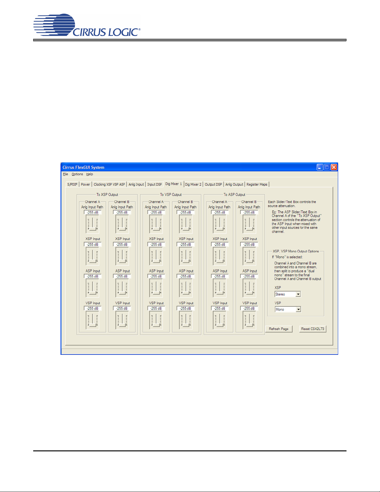
4.3.6 Digital Mixer 1 Tab
Figure 11. The “Digital Mixer 1” Tab in FlexGUI for the CDB42L73
The “Digital Mixer 1” tab contains the main controls for setting the digital mixing/routing options for all three
serial ports of the CS42L73. A brief description of each control group is described below.
• To XSP Output - register controls to configure the mix of all the input signals to the Auxiliary Serial Port
• To VSP Output - register controls to configure the mix of all the input signals to the Voice Serial Port
• To ASP Output - register controls to configure the mix of all the input signals to the Audio Serial Port
• XSP, VSP Mono Output Options - register controls to select either stereo or dual-mono mode for the
Auxiliary and Voice Serial Port outputs
• Refresh Page - reads all registers in all devices and updates the values in the GUI
• Reset CS42L73 - resets the CS42L73
CDB42L73
DS882DB1 19
Page 20

4.3.7 Digital Mixer 2 Tab
Figure 12. The “Digital Mixer 2” Tab in FlexGUI for the CDB42L73
The “Digital Mixer 2” tab contains the main controls for setting the digital signal mixing/routing to the analog outputs of CS42L73. A brief description of each control group is described below.
• To Headphone/Line Out - register controls to configure the mix of all the input signals to the headphone
or line outputs
• To Spkphone - register controls to configure the mix of all the input signals to the speakerphone output
• To Earspk/Spkphone LO - register controls to configure the mix of all the input signals to the earphone
or speakerphone-line outputs
• Input Selection Options for Spkphone and Earspk/Spkphone LO - register controls to select either Channel A from the stereo mix, Channel B from the stereo mix, or the dual-mono mix to the speakerphone,
earphone, and speakerphone-line outputs
• Refresh Page - reads all registers in all devices and updates the values in the GUI
• Reset CS42L73 - resets the CS42L73
CDB42L73
20 DS882DB1
Page 21
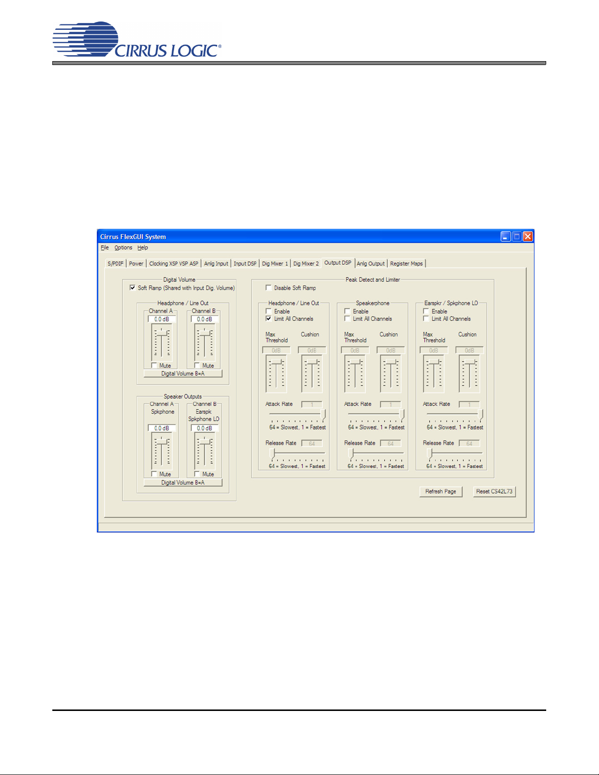
4.3.8 Output DSP Tab
Figure 13. The “Output DSP” Tab in FlexGUI for the CDB42L73
The “Output DSP” tab contains the main controls for setting the digital signal processing applied to the
analog outputs of the CS42L73. A brief description of each control group is described below.
• Digital Volume - register controls to configure the digital volume of the audio routed to the peak detect
and limiter circuitry prior to the analog outputs
• Peak Detect and Limiter - register controls to configure the peak detection and limiter functions applied
to the analog outputs
• Refresh Page - reads all registers in all devices and updates the values in the GUI
• Reset CS42L73 - resets the CS42L73
CDB42L73
DS882DB1 21
Page 22
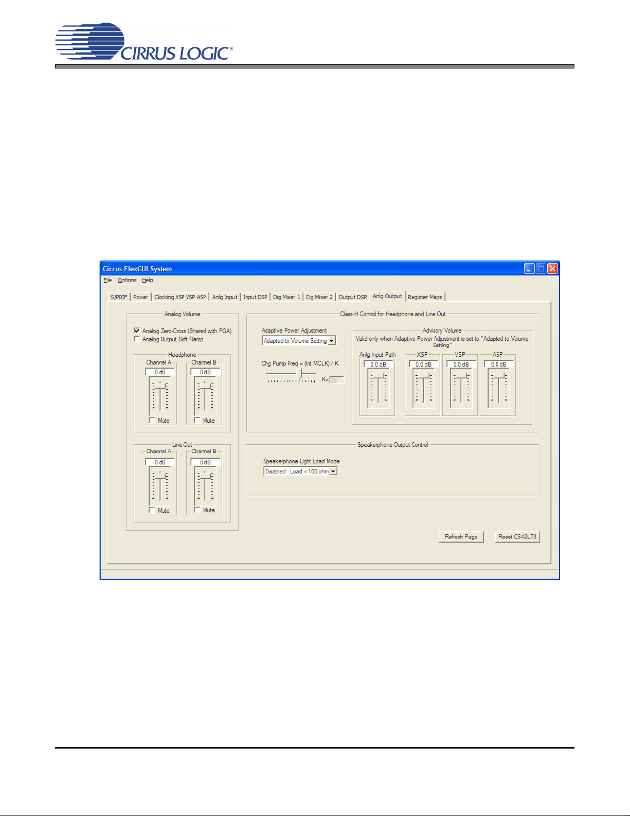
4.3.9 Analog Output Tab
Figure 14. The “Analog Output” Tab in FlexGUI for the CDB42L73
The “Analog Output” tab contains the main controls for setting the analog output circuitry options of the
CS42L73. A brief description of each control group is described below.
• Analog Volume - register controls to configure the analog volume settings of the CS42L73’s analog outputs
• Class H controls for Headphone and Line Out - register controls to configure the Class H power mode
related options and the charge pump frequency
• Speakerphone Output Control - register control to select the drive capability of the speakerphone output
• Refresh Page - reads all registers in all devices and updates the values in the GUI
• Reset CS42L73 - resets the CS42L73
CDB42L73
22 DS882DB1
Page 23
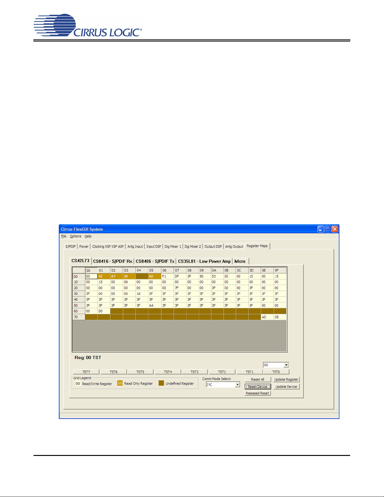
4.4 The Register Map
Figure 15. The “Register Maps” Tab in FlexGUI for the CDB42L73
The register map shows the entire user configurable register space for all programmable devices on the
CDB42L73.
It is especially useful for reading/writing a device’s register settings directly, one whole register at a time.
For example, the default value for register 0x11 is 0x15 (Figure 15). To modify register 0x11’s value, first
navigate to it by locating the cell at the intersection of row “10” and column “01.” Click on the cell and simply
type the desired hexadecimal value for that register, then press the return key (Enter) on the keyboard.
To modify one bit of a register at a time, navigate to the desired register cell, click it, then click on the applicable bits shown in the lower part of the register map page to toggle them.
Other useful controls:
• Reset All - clicking this button asserts reset to all devices on the CDB42L73
• Reset Device - clicking this button asserts reset to the device currently in view in the register map
• Released Reset - clicking this button holds/releases the device currently in view in the register map
in/from reset.
• Update Register - clicking this button refreshes the current selected register value
• Update Device - clicking this button refreshes all register values of the device currently in view in the
register map
CDB42L73
DS882DB1 23
Page 24
DS882DB1 24
USB
+5V, GND
(Bind. Post)
VA, VP, VCP, VL, VD_FILT
(Bind. Post)
Battery – VP only
(Header)
Regulators
Power Source Selection (Headers)
CS42L73
Current Sense Resistors for Power Measurement (Bypassable)
S/PDIF In
(Optical)
S/PDIF In
(RCA)
S/PDIF Out
(Optical)
S/PDIF In
(RCA)
CS8416
CS8406
Clocks
And
Data
Selection
(Headers)
Micro-
Controller
Canned
Oscillator
I2C and Board
Controls
Line In Stereo
(RCA)
Mic In 1 and 2
(1/8")
Digital Mic In
(Header)
Headphone Out
(1/8")
Lineout Stereo
(RCA)
Spkphone Out
(Term. Block & 1/8")
Spkphone/Line Out
(Term. Block & 1/8")
Earphone Out
(Term. Block & 1/8")
Direct External Digital
I/O
Figure 16. System Block Diagram
5. SCHEMATICS AND LAYOUT
CDB42L73
Page 25
DS882DB1 25
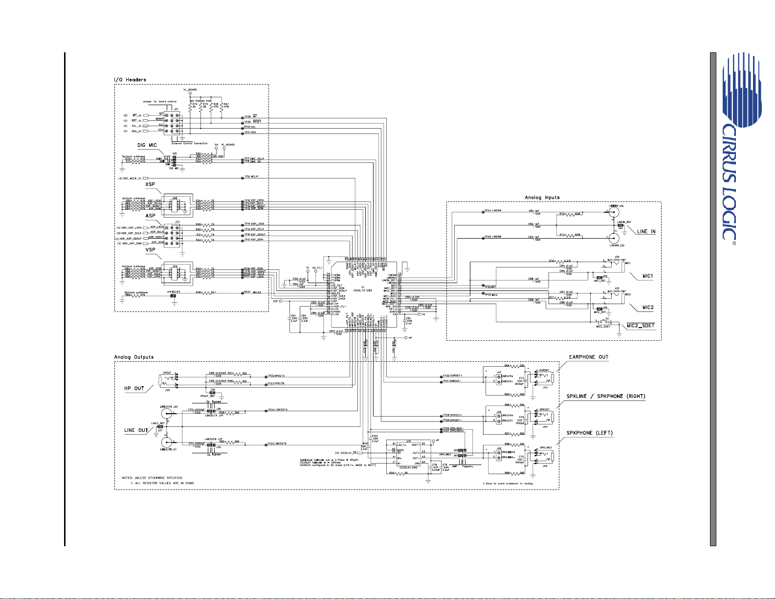
Figure 17. CS42L73
CDB42L73
Page 26

DS882DB1 26
Figure 18. USB and Microcontroller
CDB42L73
Page 27

DS882DB1 27
Figure 19. S/PDIF Receiver and Transmitter; Clock Buffers
CDB42L73
Page 28

DS882DB1 28
Figure 20. Power
CDB42L73
Page 29

DS882DB1 29
Figure 21. Top Side Silkscreen
CDB42L73
Page 30

DS882DB1 30
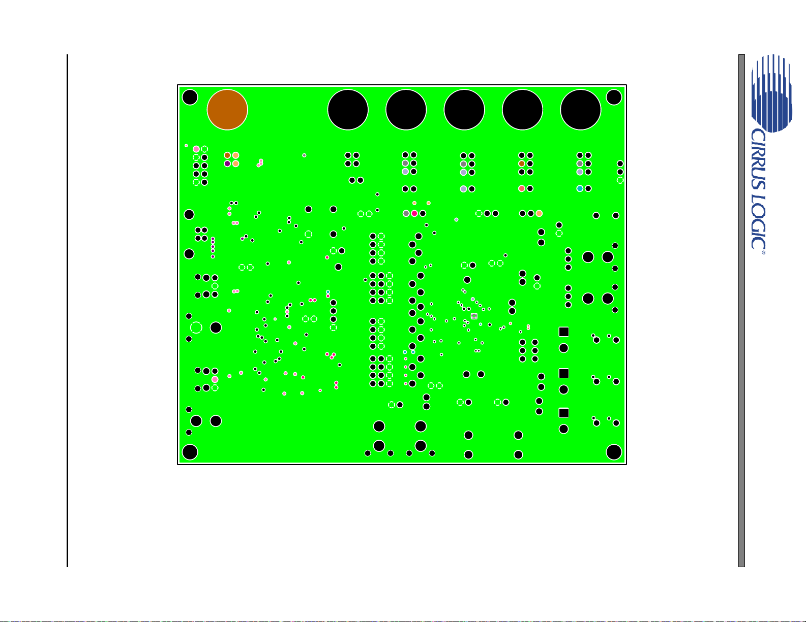
Figure 22. Layer 1
CDB42L73
Page 31

DS882DB1 31
Figure 23. Layer 2
CDB42L73
Page 32

DS882DB1 32
Figure 24. Layer 3
CDB42L73
Page 33
DS882DB1 33
Figure 25. Layer 4
CDB42L73
Page 34
DS882DB1 34
Figure 26. Layer 5
CDB42L73
Page 35
DS882DB1 35
Figure 27. Layer 6
CDB42L73
Page 36
6. REVISION HISTORY
Contacting Cirrus Logic Support
For all product questions and inquiries, contact a Cirrus Logic Sales Representative.
To find the one nearest you, go to www.cirrus.com.
IMPORTANT NOTICE
Cirrus Logic, Inc. and its subsidiaries ("Cirrus") believe that the information contained in this document is accurate and reliable. However, the information is subject
to change without notice and is provided "AS IS" without warranty of any kind (express or implied). Customers are advised to obtain the latest version of relevant
information to verify, before placing orders, that information being relied on is current and complete. All products are sold subject to the terms and conditions of sale
supplied at the time of order acknowledgment, including those pertaining to warranty, indemnification, and limitation of liability. No responsibility is assumed by Cirrus
for the use of this information, including use of this information as the basis for manufacture or sale of any items, or for infringement of patents or other rights of third
parties. This document is the property of Cirrus and by furnishing this information, Cirrus grants no license, express or implied under any patents, mask work rights,
copyrights, trademarks, trade secrets or other intellectual property rights. Cirrus owns the copyrights associated with the information contained herein and gives consent for copies to be made of the information only for use within your organization with respect to Cirrus integrated circuits or other products of Cirrus. This consent
does not extend to other copying such as copying for general distribution, advertising or promotional purposes, or for creating any work for resale.
CERTAIN APPLICATIONS USING SEMICONDUCTOR PRODUCTS MAY INVOLVE POTENTIAL RISKS OF DEATH, PERSONAL INJURY, OR SEVERE PROPERTY OR ENVIRONMENTAL DAMAGE (“CRITICAL APPLICATIONS”). CIRRUS PRODUCTS ARE NOT DESIGNED, AUTHORIZED OR WARRANTED FOR USE
IN PRODUCTS SURGICALLY IMPLANTED INTO THE BODY, AUTOMOTIVE SAFETY OR SECURITY DEVICES, LIFE SUPPORT PRODUCTS OR OTHER CRITICAL APPLICATIONS. INCLUSION OF CIRRUS PRODUCTS IN SUCH APPLICATIONS IS UNDERSTOOD TO BE FULLY AT THE CUSTOMER’S RISK AND CIRRUS DISCLAIMS AND MAKES NO WARRANTY, EXPRESS, STATUTORY OR IMPLIED, INCLUDING THE IMPLIED WARRANTIES OF MERCHANTABILITY AND
FITNESS FOR PARTICULAR PURPOSE, WITH REGARD TO ANY CIRRUS PRODUCT THAT IS USED IN SUCH A MANNER. IF THE CUSTOMER OR CUSTOMER’S CUSTOMER USES OR PERMITS THE USE OF CIRRUS PRODUCTS IN CRITICAL APPLICATIONS, CUSTOMER AGREES, BY SUCH USE, TO FULLY
INDEMNIFY CIRRUS, ITS OFFICERS, DIRECTORS, EMPLOYEES, DISTRIBUTORS AND OTHER AGENTS FROM ANY AND ALL LIABILITY, INCLUDING ATTORNEYS’ FEES AND COSTS, THAT MAY RESULT FROM OR ARISE IN CONNECTION WITH THESE USES.
Cirrus Logic, Cirrus, and the Cirrus Logic logo designs are trademarks of Cirrus Logic, Inc. All other brand and product names in this document may be trademarks
or service marks of their respective owners.
Release Changes
DB1 Initial Release
CDB42L73
36 DS882DB1
 Loading...