

Page 1
Evaluation Board for CS4270
CDB4270
Features
Single-Ended Analog Audio Inputs and Outputs
CS8416 S/PDIF Digital Audio Receiver
Header for External Configuration of CS4270
Header for External DSP Serial Audio I/O
3.3V Logic Interfaces
Pre-Defined Software Scripts
Demonstrates Recommended Layout
Windows
Configuration and Control
®
-Compatible GUI Interface for Board
Description
Using the CDB4270 is an excellent way to evaluate the
CS4270 CODEC. Other equipment required includes
analog/digital audio sources/analyzer, a 5V power supply and a Windows-compatible
PC for the GUI.
System timing for the I²S, Left-Justified or Right-Justi-
fied audio data formats can be provided by the CS4270,
by the CS8416, or by a device connected to the onboard DSP I/O header. The evaluation board may also
be configured to accept external timing and data signals
for operation in a user application during system
development.
RCA jacks are provided for the analog audio inputs and
outputs. Digital S/PDIF transmit or receive data I/O is
available via either RCA jacks or optical connectors.
The Windows GUI software provided allows for easy
configuration of the CDB4270. The GUI software communicates with the board via USB or serial port
connections to configure the CS4270 registers.
ORDERING INFORMATION
CDB4270 Evaluation Board
CS8406
S/PDIF
Output
CS8416
S/PDIF
Input
Osc.
http://www.cirrus.com
Hardware
Setup
Clocks/Data
MCLK BUS
Hardware
Setup
Clocks
/Data
DSP HEADER
FPGA
ADC/DAC Clocks & Data
Serial/USB Control Port
I2C/SPI Header
ADC/DAC
Clocks/
Data
Hardware
Setup
Copyright © Cirrus Logic, Inc. 2006
CS4270
HW Setup
Switches
(All Rights Reserved)
ANALOG INPUT
Single-Ended Input
ANALOG OUTPUT
Single-Ended
Output
SEPTEMBER '06
DS686DB3
Page 2

TABLE OF CONTENTS
1. SYSTEM OVERVIEW ............................................................................................................................. 5
1.1 Power ............................................................................................................................................... 5
1.2 Grounding and Power Supply Decoupling ...................... ... .... ... ... ... ... .... ........................................... 5
1.3 FPGA ................................................................................................................................................ 5
1.4 CS4270 Audio CODEC .................................................................................................................... 5
1.5 CS8406 Digital Audio Transmitter ............... ... ... ... .... .......................................... ... ... ........................ 5
1.6 CS8416 Digital Audio Receiver ...................... ... ... .... ... ... ... .... ......................................... .... .............. 5
1.7 Canned Oscillator ............................................................................................................................. 6
1.8 External Control Headers ................................................................................................................. 6
1.9 Analog Input ..................................................................................................................................... 6
1.10 Analog Outputs ............................................................................................................................... 8
1.11 Control Port .................................................................................................................................... 8
1.12 Hardware Mode Switches ............................................................................................................... 8
2. FPGA OVERVIEW .................................................................................................................................. 9
2.1 FPGA Architecture ............................................................................................................................ 9
2.2 Internal Sub-Clock Routing ............................................................................................................... 9
2.3 Internal Data Routing ...................................................................................................................... 10
2.4 Internal Drivers ............................................................................................................................... 11
2.5 External MCLK Control ................................................................................................................... 12
3. SOFTWARE MODE .............................................................................................................................. 13
3.1 CDB4270 Control Scripts ............................................................................................................... 13
3.1.1 S/PDIF In, Analog Out ........................................................................................................... 13
3.1.2 Analog In, S/PDIF Out .............................. ... .... ... ... ....................................... ... ... ... .... ... ......... 13
3.1.3 Analog In, Analog Out (Digital Loop-Back) ............................ ... .... ... ... ... .... ............................ 13
3.1.4 DSP In, Analog Out ............................................................................................................... 13
3.2 CDB4270 GUI ................................................................................................................................. 14
3.3 Register Maps Control Tabs ........................................................................................................... 15
4. HARDWARE MODE ............................................................................................................................. 18
5. FPGA GUI REGISTER DESCRIPTION ................................................................................................ 18
5.1 FPGA REGISTER QUICK REFERENCE ....................................................................................... 18
5.2.1 Revision Number Bits (Bits 7:0) ............................................... .... ......................................... 19
5.3.1 SDOUT Routing to Header (Bits 7:6) .................................................................................... 20
5.3.2 MCLK Source (Bit 4) .......................................... ... ... ....................................... ... ... .... ... ......... 20
5.3.3 SDOUT Routing to DUT (Bits 3:2) ......................................................................................... 20
5.3.4 Subclock Routing (Bits 1:0) ... ... ... ... .... ... ... ... .... ... ... ... .... ......................................... .... ... ......... 21
5.4.1 CS8406 OMCLK Divider Control (Bits 7:6) ........................................................................... 21
5.4.2 CS8406 Master/Slave Select (Bit 4) ...................................................................................... 22
5.4.3 CS8406 SDIN Format Select (Bit 3) ...................................................................................... 22
5.4.4 CS8406 SDIN Source (Bits 1:0) ......................... ................................................................ ...22
5.5.1 CS8416 RMCLK Divider Control (Bit 6) ................................................................................ 23
5.5.2 CS8416 Master/Slave Select (Bit 4) ...................................................................................... 23
5.5.3 CS8416 SDOUT Format Select (Bit 3) .................................................................................. 23
6. CDB4270 HARDWARE MODE SETTINGS ......................................................................................... 24
7. CDB CONNECTORS, SWITCHES, INDICATORS AND JUMPERS ................................................... 26
8. ADC PERFORMANCE PLOTS ............... ... ... .... ... ... ... .......................................... .... ... ......................... 27
9. DAC PERFORMANCE PLOTS ............... ... ... .... ... ... ... .......................................... .... ... ......................... 31
10. CDB BLOCK DIAGRAM ................................................................................................................ 36
11. CDB SCHEMATICS ............................................................................................................................ 37
12. CDB LAYOUT ..................................................................................................................................... 46
13. CHANGES MADE TO REV. B BOARD ............................................................................................. 49
13.1 Modifications (Done by Cirrus Logic) .......................................................................................... 49
14. REVISION HISTORY .......................................................................................................................... 50
CDB4270
2 DS686DB3
Page 3

LIST OF FIGURES
Figure 1.ADC THD+N ................................................................................................................................. 7
Figure 2.ADC Dynamic Range .................................................................................................................... 7
Figure 3.Internal Sub-Clock Routing ........................................................................................................... 9
Figure 4.Internal Data Routing .................................................................................................................. 10
Figure 5.Internal Drivers ............................................................................................................................ 11
Figure 6.External MCLK Control ............................................................................................................... 12
Figure 7.CDB4270 Controls Tab ............................................................................................................... 14
Figure 8.Register Maps Tab - CS4270 ..................................................................................................... 15
Figure 9.Register Maps Tab - Board Configuration .................................................................................. 16
Figure 10.Register Maps Tab - GPIO ....................................................................................................... 17
Figure 11.FFT (-1 dB 48 kHz) ................................................................................................................... 27
Figure 12.FFT (-60 dB, 48 kHz) ................................................................................................................ 27
Figure 13.FFT (48 kHz, No Input) ............................................................................................................. 27
Figure 14.48 kHz, THD+N vs. Input Freq .................................................................................................. 27
Figure 15.48 kHz, THD+N vs. Level ......................................................................................................... 27
Figure 16.48 kHz, Fade-to-Noise Linearity ............................................................................................... 27
Figure 17.48 kHz, Frequency Response ................................................................................................... 28
Figure 18.48 kHz, Crosstalk ...................................................................................................................... 28
Figure 19.FFT (-1 dB 96 kHz) ................................................................................................................... 28
Figure 20.FFT (-60 dB, 96 kHz) ................................................................................................................ 28
Figure 21.FFT (96 kHz, No Input) ............................................................................................................. 28
Figure 22.96 kHz, THD+N vs. Input Freq .................................................................................................. 28
Figure 23.96 kHz, THD+N vs. Level ......................................................................................................... 29
Figure 24.96 kHz, Fade-to-Noise Linearity ............................................................................................... 29
Figure 25.96 kHz, Frequency Response ................................................................................................... 29
Figure 26.96 kHz, Crosstalk ...................................................................................................................... 29
Figure 27.FFT (-1 dB 192 kHz) ................................................................................................................. 29
Figure 28.FFT (192 kHz, -60 dB) .............................................................................................................. 29
Figure 29.FFT (192 kHz, No Input) ........................................................................................................... 30
Figure 30.192 kHz, THD+N vs. Input Freq ................................................................................................ 30
Figure 31.192 kHz, THD+N vs. Level ....................................................................................................... 30
Figure 32.192 kHz, Fade-to-Noise Linearity ............................................................................................. 30
Figure 33.192 kHz, Frequency Response ................................................................................................. 30
Figure 34.192 kHz, Crosstalk .................................................................................................................... 30
Figure 35.FFT (48 kHz, 0 dB) ................................................................................................................... 31
Figure 36.FFT (48 kHz, -60 dB) ................................................................................................................ 31
Figure 37.FFT (48 kHz, No Input) ............................................................................................................. 31
Figure 38.FFT (48 kHz Out-of-Band, No Input) ......................... ... .... ... ... ... ... .... ... ... ... .... ... ......................... 31
Figure 39.48 kHz, THD+N vs. Input Freq .................................................................................................. 31
Figure 40.48 kHz, THD+N vs. Level ......................................................................................................... 31
Figure 41.48 kHz, Fade-to-Noise Linearity ............................................................................................... 32
Figure 42.48 kHz, Frequency Response ................................................................................................... 32
Figure 43.48 kHz, Crosstalk ...................................................................................................................... 32
Figure 44.48 kHz, Impulse Response ....................................................................................................... 32
Figure 45.FFT (96 kHz, 0 dB) ................................................................................................................... 32
Figure 46.FFT (96 kHz, -60 dB) ................................................................................................................ 32
Figure 47.FFT (96 kHz, No Input) ..............................................................................................
Figure 48.FFT (96 kHz Out-of-Band, No Input) ......................... ... .... ... ... ... ... .... ... ... ... .... ... ......................... 33
Figure 49.96 kHz, THD+N vs. Input Freq .................................................................................................. 33
Figure 50.96 kHz, THD+N vs. Level ......................................................................................................... 33
Figure 51.96 kHz, Fade-to-Noise Linearity ............................................................................................... 33
Figure 52.96 kHz, Frequency Response ................................................................................................... 33
CDB4270
............... 33
DS686DB3 3
Page 4

CDB4270
Figure 53.96 kHz, Crosstalk .. .... ... ... ... .... ... ................................................................................................ 34
Figure 54.96 kHz, Impulse Response ................................. ...................................................................... 34
Figure 55.FFT (192 kHz, 0 dB) ................................................................................................................. 34
Figure 56.FFT (192 kHz, -60 dB) .............................................................................................................. 34
Figure 57.FFT (192 kHz, No Input) ........................................................................................................... 34
Figure 58.FFT (192 kHz Out-of-Band, No Input) ....................................................................................... 34
Figure 59.192 kHz, THD+N vs. Input Freq ................................................................................................ 35
Figure 60.192 kHz, THD+N vs. Level ....................................................................................................... 35
Figure 61.192 kHz, Fade-to-Noise Linearity ............................................................................................. 35
Figure 62.192 kHz, Frequency Response ................. .......... ......... .......... .......... ......... .......... .......... ............ 35
Figure 63.192 kHz, Crosstalk .................................................................................................................... 35
Figure 64.192 kHz, Impulse Response ..................................................................................................... 35
Figure 65.Block Diagram ........................................................................................................................... 36
Figure 66.CS4270 .... .... ... ... ... .... ... ... ... .......................................... .... ... ...................................................... 37
Figure 67.Analog Input .... ... ... .......................................... .... ... .......................................... ... ...................... 38
Figure 68.Analog Output ....... .... ... ... ... .......................................... .... ... ...................................................... 39
Figure 69.CS8406 S/PDIF Transmitter ..................................................................................................... 40
Figure 70.CS8416 S/PDIF Receiver ............... ... .... ... ... ... .... ... ... ... .... ... ... ... ... .... ... ... ................................... 41
Figure 71.Buffers - Clock/Data Routing .................................................................................................... 42
Figure 72.FPGA ........................ ... ... ... .... ... ... ... .......................................................................................... 43
Figure 73.USB/RS232 Microprocessor .................................................................................. ... .... ............ 44
Figure 74.Power . ....................................................................................................................................... 45
Figure 75.Silk Screen ... .......................................... ... ... ... .... ... ... ... ............................................................. 46
Figure 76.Top-Side Layer ...................................................... ... ... .... ... ... ... ................................................ 47
Figure 77.Bottom-Side Layer .......................... ... .... ... ... ... .... ... ... ... .... ... ... ... ... .... ... ... ... .... ............................ 48
LIST OF TABLES
Table 1. Revision Number ......................................................................................................................... 19
Table 2. SDOUT Routing to Header ......................................................................................................... 20
Table 3. MCLK Source .............................................................................................................................. 20
Table 4. SDOUT Routing to DUT .............................................................................................................. 20
Table 5. Sub-Clock Routing ...................................................................................................................... 21
Table 6. CS8406 OMCLK Frequency ....................................................................................................... 21
Table 7. CS8406 Master/Slave ................................................................................................................. 22
Table 8. CS8406 SDIN Format ................................................................................................................. 22
Table 9. CS8406 SDIN Source ................................................................................................................. 22
Table 10. CS8416 RMCLK Frequency ...................................................................................................... 23
Table 11. CS8416 Master/Slave ............................................................................................................... 23
Table 12. CS8416 SDOUT Format ........................................................................................................... 23
Table 13. CDB4270 Hardware Mode - Functional Description ................................................................. 24
Table 14. Connectors and Switches ......................................................................................................... 26
Table 15. Jumpers and Indicators ............................................................................................................. 26
4 DS686DB3
Page 5

CDB4270
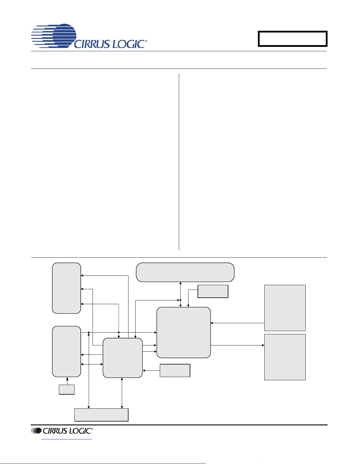
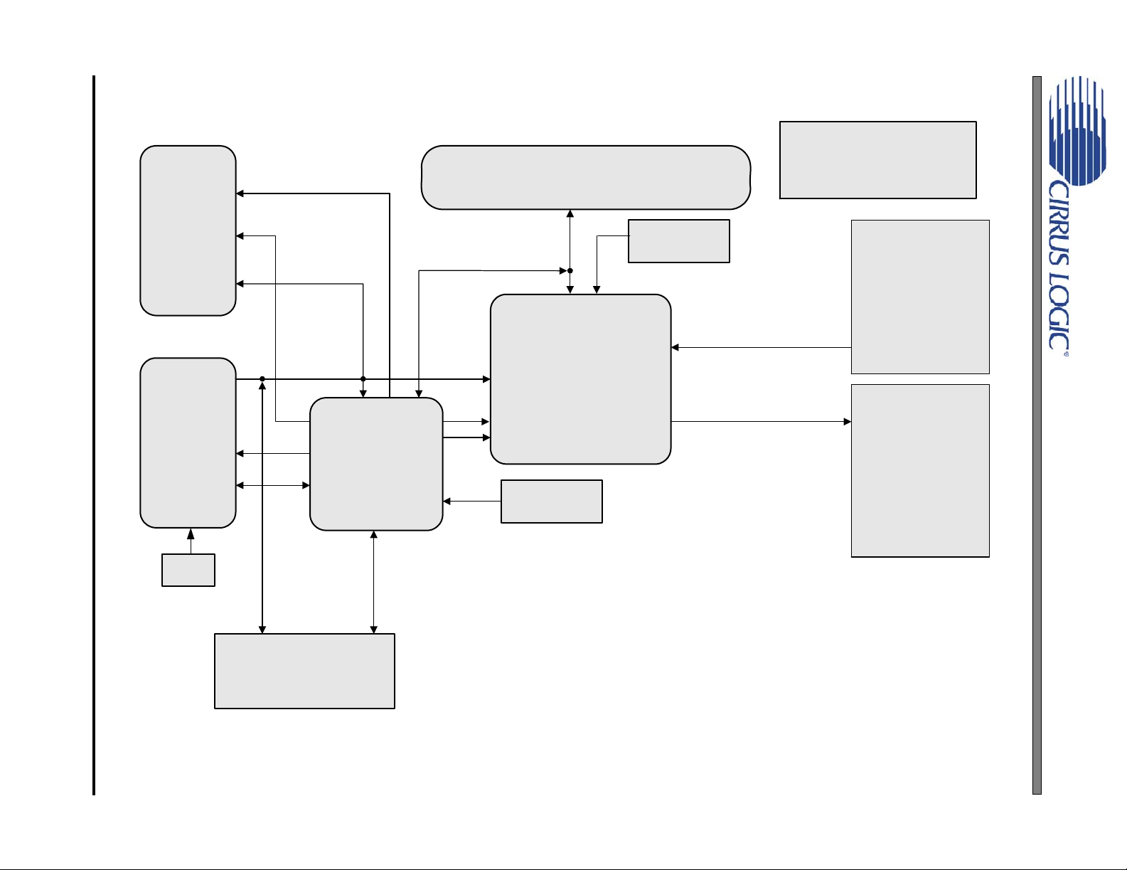
1. SYSTEM OVERVIEW
The CDB4270 evaluation board is an excellent tool for evaluating the CS4270 CODEC. The board features both
analog and digital audio interfaces along with an FPGA for data/clk routing and an on-board microprocessor for configuration control. The board is easily configured in Software Mode using the supplied PC-to-DUT USB cable along
with the Windows-based GUI configuration software or in Hardware Mode using the on-board dip switches.
The CDB4270 schematic set has been partitioned into nine pages and is shown in Figures 66 through 74.
1.1 Power
Power must be supplied to the evaluation board through the +5.0 V binding posts. The +5 V inputs must be
referenced to the single black binding post ground connector (Figure 74 on page 45).
WARNING: Please refer to the CS4270 data sheet for allowable voltage levels.
1.2 Grounding and Power Supply Decoupling
To optimize performance, PC board designs for the CS4270 require careful attention to power supply,
grounding and signal routing arrangements. Figure 65 on page 36 shows the basic compon ent/signal interconnect for the CDB4270. Figure 75 on page 46 shows the component placement. Figure 76 on page 47
shows the top layout. Figure 77 on page 48 shows the botto m layout. The decoupling capacitors are loca ted
as close to the CS4270 as possible. Extensive use of ground plane fill in the evaluation board yields large
reductions in radiated noise.
1.3 FPGA
See “F PGA Overview” on page 9 for a complete description of the FPGA (Figure 72 on page 43) that is used
on the CDB4270.
1.4 CS4270 Audio CODEC
A complete description of the CS4270 (Figure 66 on page 37) is included in the CS4270 product data sheet.
The CS4270 codec performs stereo 24-bit A/D and D/A conversion at sample rates of up to 216 KHz. The
part accommodates I²S, Left-Justifie d an d Rig ht -Ju st if ied ser ial au dio for m ats .
1.5 CS8406 Digital Audio Transmitter
A complete description of the CS8406 transmitter ( Figure 69 on page 40 ) and a discussion of the d igital audio interface are included in the CS8406 data sheet.
The CS8406 converts the PCM data from either the CS4 270, the DSP Header, or the CS8416 to a standard
S/PDIF data stream. The CS8406 operates in either master or slave sub-clock mode and will accept either
a 128 Fs, 256 Fs, or 512 Fs master clock on the OMCK input pin. The device will operate in either the LeftJustified or I²S interface data modes.
1.6 CS8416 Digital Audio Receiver
A complete description of the CS8416 receiver (Figure 70 on page 41) and a discussion of the digital audio
interface are included in the CS8416 data sheet.
The CS8416 converts the input S/PDIF data stream into PCM data that can be used by the CS4270 and
CS8406. The device operates in either Master or Slave su b-clo ck modes and gen er ates eith er a 128 Fs or
256 Fs master clock for output on the RMCK pin. Either Left-Justified or I²S interface output data formats
can be selected
DS686DB3 5
Page 6

1.7 Canned Oscillator
Oscillator Y1 provides a system master clock. This clock is routed through the CS8416 and out of the RMCK
pin when the S/PDIF input is disconnected (refer to the CS8416 data sheet for details on OMCK opera tion).
To use the canned oscillator as the source of the MCLK signal, remove the S/PDIF input to the CS8416 and
configure the CS8416 appropriately.
The oscillator is mounted in pin sockets, allowing easy removal or replacement. The board is shipped with
a 12.288 MHz crystal oscillator populated at Y1.
1.8 External Control Headers
The evaluation board has been designed to allow interfacing with external systems via the J10 and J9 headers.
The 10-pin, 2-row header, J9, allows access to the serial audio signa ls required to interface with a DSP (see
Figure 71 on page 42).
The 18-pin, 3-row header, J10, allows the user bidirectional acce ss to the SPI
ply removing all of the shunt jumpers from the “NORMAL” position. The user may then choose to connect
a ribbon cable to the “EXTERNAL” position. A single “GND” row for the ribbon cable’s ground connection is
provided to maintain signal integrity. Two unpopulated pull-up resistors are also available should the user
choose to use the CDB for the I²C power rail.
CDB4270
TM
/I²C® control signals by sim-
1.9 Analog Input
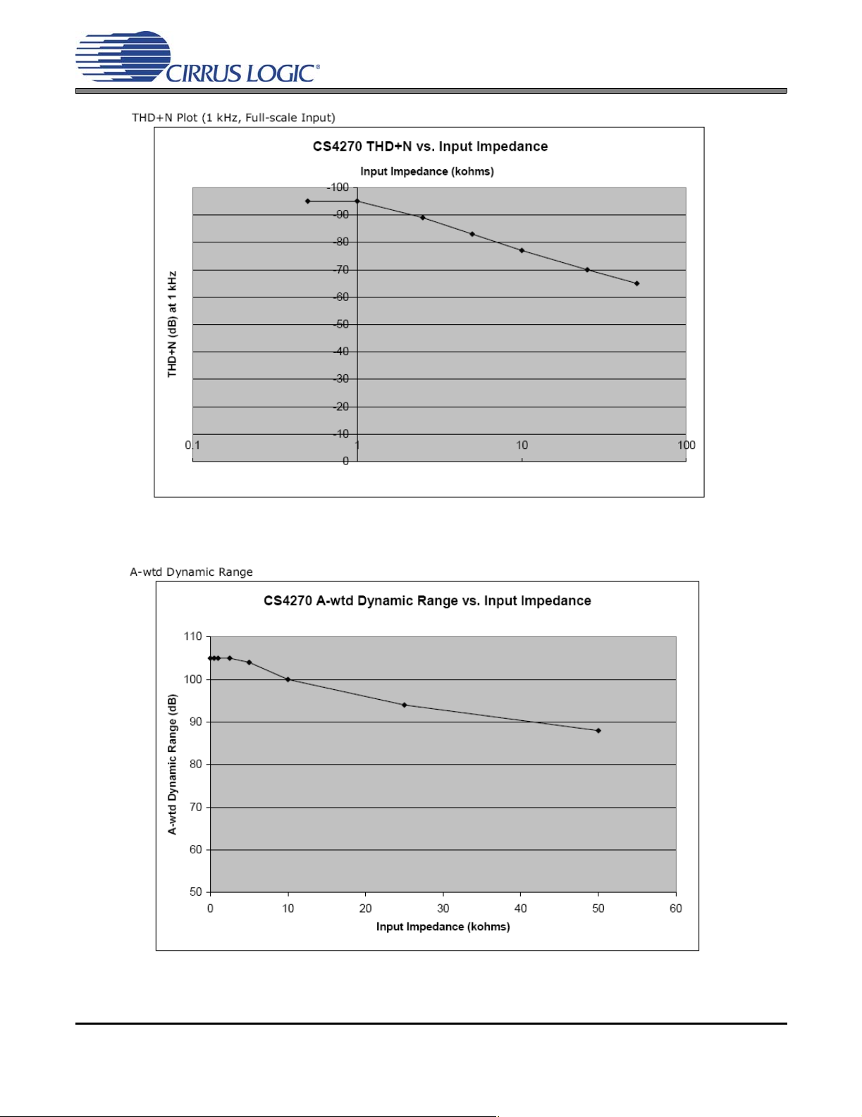
RCA connectors supply the CS4270 analog inputs through passive, AC-coupled, single-ended circuits. A
2 Vrms single-ended signal into the RCA connectors will drive the CS4270 inputs to full scale (1 Vrms). The
input network on the CDB4270 was designed to demonstrate that the CS4270 will provide superior performance with up to 2.5 kΩ driving impedances (looking back from the CS4270 inputs) while allowing for
2 Vrms inputs. ADC performance varies depending upon the input impedance of the input network.
Figures 1 and 2 show typical THD+N and Dynamic Range performance for the ADC as a function of input
impedance.
6 DS686DB3
Page 7
CDB4270
Figure 1. ADC THD+N
Figure 2. ADC Dynamic Range
DS686DB3 7
Page 8

1.10 Analog Outputs
The CS4270 analog outputs are AC-coupled and routed through a single-pole RC Low-Pass filter.
1.11 Control Port
A graphical user interface is included with the CDB 4270 to allow easy manipu lation of the registers in th e
CS4270 (see the CS4270 data sheet for register descriptions and the “FPGA GUI Regi ster Descr iption” on
page 18). The GUI will run on a standard Windows-based PC. Connecting a USB cable from a PC to J15
or an RS-232 cable to J16 and launching the Cirrus Logic FlexGUI software enab les control and configur ation of the board.
Refer to “Software Mode” on page 13 for a description of the Graphical User Interface (GUI).
1.12 Hardware Mode Switches
The “HW Mode Config” and ”Clk/Data Config” switches control all Hardware Mode options. “Hardware
Mode” on page 18 provides a description of each topology.
CDB4270
8 DS686DB3
Page 9
CDB4270
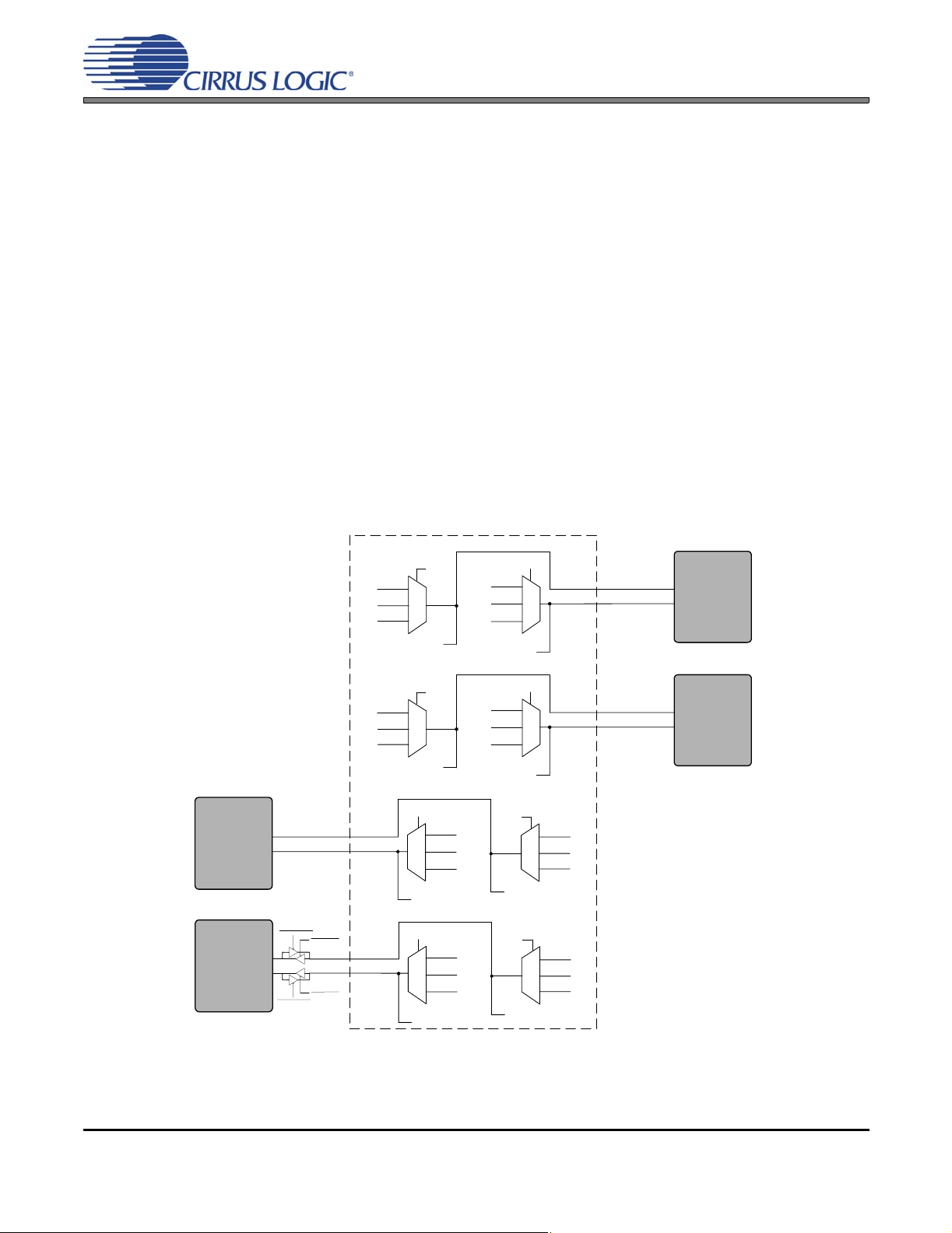
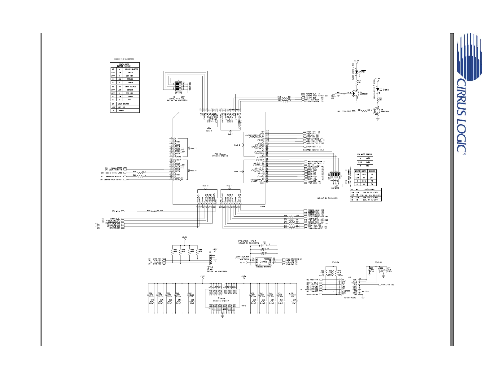
2. FPGA OVERVIEW
The FPGA (U11) controls all digital signal routing between the CS4270, CS8406, CS8416 and the DSP I/O Header.
The device also generates all of the clock/data driver output enables and S/PDIF device mode controls. The FPGA
internal registers can be configured either via the I² C (Software Mode) or via external dip switches (Hardware Mode).
When using the CS4270 in Hardware Mode, the FPGA decodes some of these dip-switch settings and generates
the CS4270 control signals. In addition, the FPGA distributes resets from the micro for all of the devices on the
board.
2.1 FPGA Architecture
Figures 3 through 5 show the internal architect ure of the FPG A. Figure 6 shows the MCLK routing to/from
the FPGA and the other devices on the board. The FPGA has an I²C interface and interna l registers for software control and can also read external dip-switch settings for hardware control. Refer to the FPGA GUI
Register Description section of this document for a description of the FPGA registers.
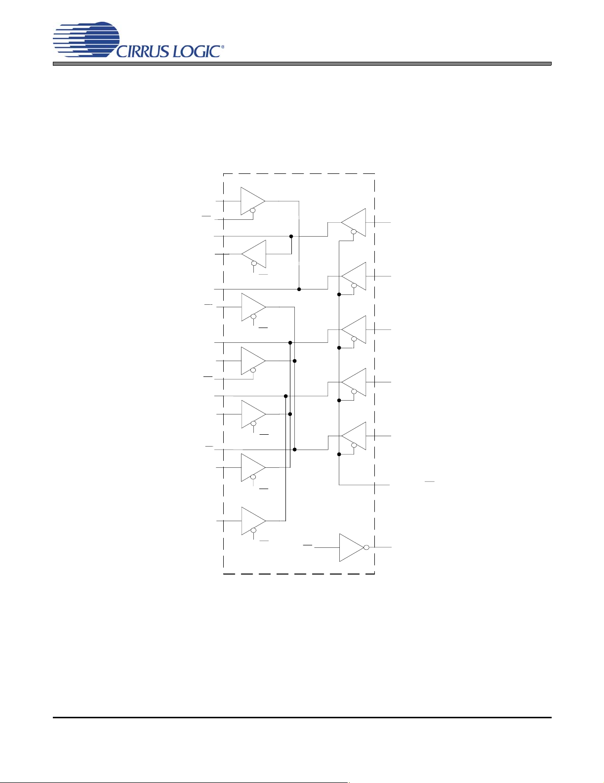
2.2 Internal Sub-Clock Routing
Figure 3 shows the internal sub-clock (SCLK, LRCK) routing topology between the CS4270, CS8416,
CS8406 and DSP Header. Refer to the FPGA GUI R egister Description section of this document for a
description of the sub-clock routing register settings.
.
FPGA
CS4270
LRCK
SCLK
CS8416-FPGA-LRCK
HDR-LRCK
FPGA-CS8406-LRCK
SUB_CK[1:0]
FPGA- DUT-LRCK
SUB_CK[1:0]
CS8416-FPGA-SCLK
HDR-SCLK
FPGA-CS8406-SCLK
FPGA-DUT-SCLK
CS8416
LRCK
SCLK
DSP Header
LRCK
SCLK
SUBCLK.FROM.HDR
SUBCLK.FROM.HDR
SUB_CK[1:0]
CS8416-FPGA-SCLK
HDR-SCLK
FPGA-DUT-SCLK
FPGA-CS8406-SCLK
SUB_CK[1:0]
FPGA-DUT-SCLK
HDR-SCLK
FPGA-CS8406-SCLK
SUB_CK[1:0]
CS8416-FPGA-SCLK
FPGA-DUT-SCLK
FPGA-CS8406-SCLK
SUBCLK.TO.HDR
SUBCLK.TO.HDR
CS8416-FPGA-LRCK
HDR-LRCK
FPGA-DUT-LRCK
FPGA-CS8406- LRCK
SUB_CK[1:0]
CS8416-FPGA-SCLK
SUB_CK[1:0]
HDR-SCLK
Figure 3. Internal Sub-Clock Routing
SUB_CK[1:0]
FPGA-DUT-LRCK
HDR-LRCK
FPGA-CS8406-LRCK
CS8416-FPGA- LRCK
CS8416-FPGA-LRCK
FPGA-DUT-LRCK
FPGA-CS8406-LRCK
HDR-LRCK
CS8406
LRCK
SCLK
DS686DB3 9
Page 10
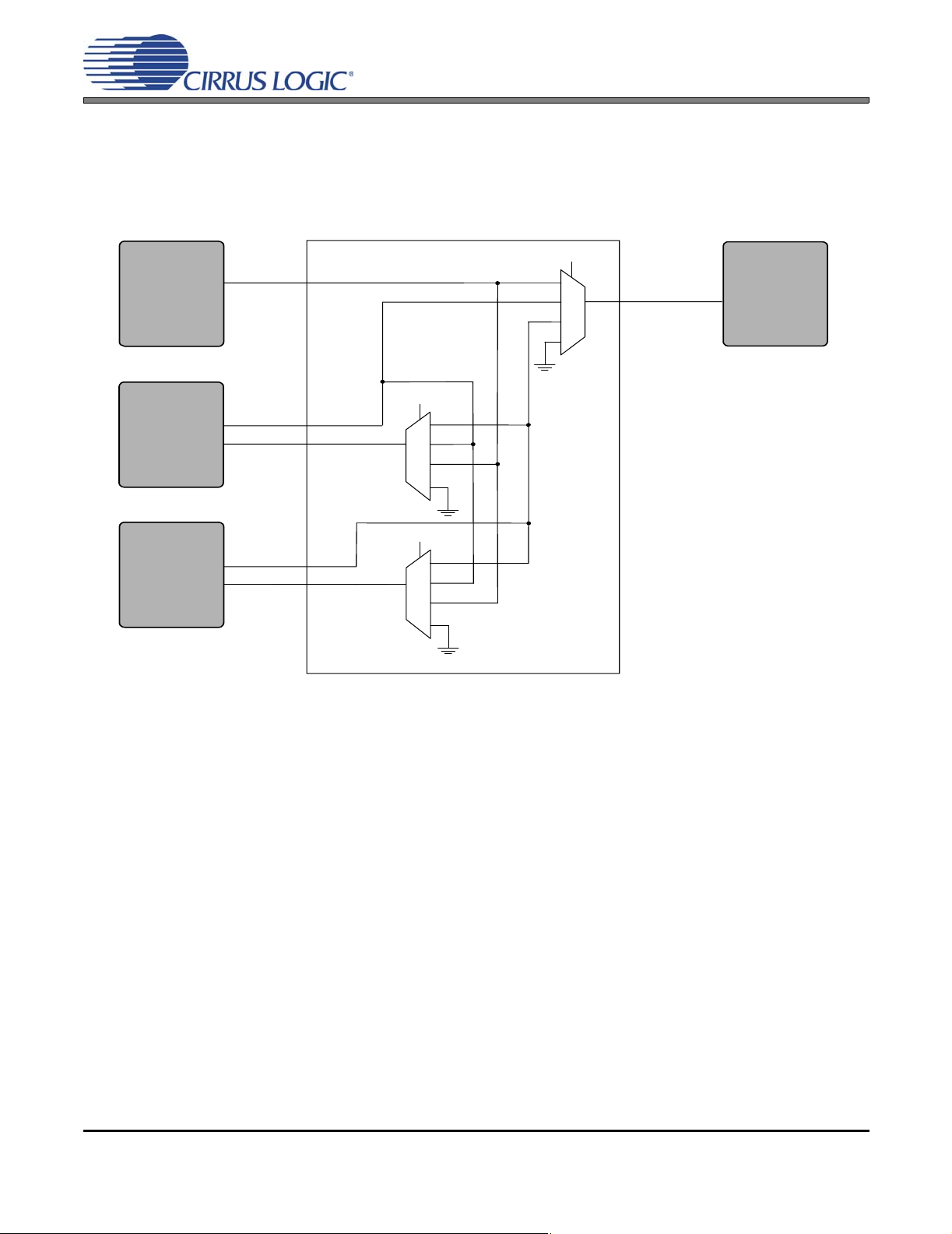
2.3 Internal Data Routing
Figure 4 shows the internal data routing topology between the CS4270, CS8416, CS8406 and the DSP
Header. Refer to the FPGA GUI Register Description section of this document for a description of the audio
data routing register settings.
.
CDB4270
CS8416
SDOUT
DSP Head er
SDIN
SDOUT
CS4270
SDOUT
SDIN
CS8416-FPGA-SDOUT
FPGA-SDIN
FPGA-HDR-SDOUT
CS4270-FPGA-SDOUT
CS4270-SDIN
FPGA
SDIO[1 :0]
DUT_SDIO[1:0]
TXSDIO [1:0]
CS8406-SDIN
CS8406
SDIN
Figure 4. Internal Data Routing
10 DS686DB3
Page 11
2.4 Internal Drivers
Figure 5 shows the internal drivers and logic for board level selects/enables and so forth. Refe r to the FPGA
GUI Register Description section of this document for a description of the board level control register set-
tings.
.
MICRO-SDA/CCLK
CDB4270
FPGA
FPGA-SPI
HDR-SDA/CDOUT
MICRO-SCL/MISO
HDR-SCL/CCLK
FPGA-CS
HDR-AD1/CDIN
FPGA-AD0
FPGA-I2C
HDR-AD2
FPGA-MOSI
HDR-AD0/CS
FPGA-AD1
FPGA-SPI
FPGA-SPI
FPGA-SPI
FPGA-I2C
M1
M0
MDIV1
MDIV2
DIF
FPGA-SW/HW
FPGA-AD2
FPGA-I2C
FPGA-I2C
I2C
Figure 5. Internal Drivers
DS686DB3 11
Page 12
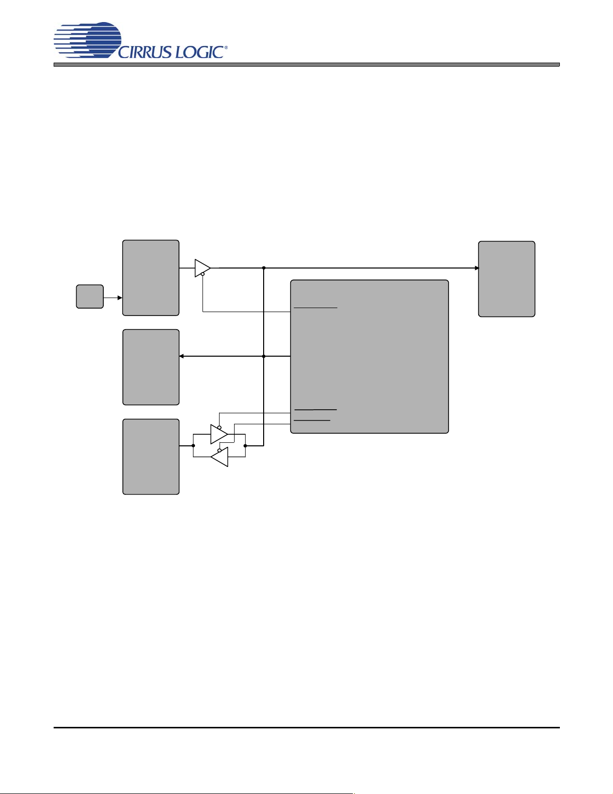
2.5 External MCLK Control
Several sources for MCLK exist on the CDB4270. The crystal oscillator, Y1, will master the MCLK bus when
no S/PDIF signal is input to the CS8416 (refer to the CS8416 data sheet for details on OMCK operation).
When S/PDIF data is present at the CS8416 input, the CS8416 generates a master clock whenever its internal PLL is locked to the incoming S/PDIF stream.
The DSP Header can master the MCLK bus or be an observation point for MCLK depe nding upon th e state
of the driver control signals from the FPGA.
Refer to the Register Description section of this document for a description of the MCLK routing co ntrol registers.
.
CDB4270
OSC
CS8416
OMCK
CS8406
DSP Header
RMCK
OMCK
MCLK
CS4270
MCLK
FPGA
MCLK.FROM.8416
MCLK
MCLK.FROM.HDR
MCLK.TO.HDR
Figure 6. External MCLK Control
12 DS686DB3
Page 13

CDB4270
3. SOFTWARE MODE
The CDB4270 uses a Microsoft Windows-based GUI (download from Cirrus web site), which allows control of the
CS4270 and FPGA registers. Interface to the GUI is provided via USB or RS-232 serial connection. Once the appropriate cable is connected between the CDB4270 and the host PC, run “FlexLoader.exe”. The software should
automatically detect the board. If a board selection dialog is displayed, select “CDB4270” from the list. Once loaded,
all registers are set to their default state. Note: The board is automatically set to Software Control Mode once the
serial or USB cable is installed and the GUI is up and running. The GUI’s “File” menu provides the ability to save
and load script files containing all of the register settings. Sample script file s for basic mode operation can be downloaded from the archive at www.cirrus.com.
3.1 CDB4270 Control Scripts
Brief descriptions of the supplied scripts are given below.
3.1.1 S/PDIF In, Analog Out
When the SPDIF_IN_AOUT.FGS script is run, the CS8416 is the sub-clock (SCLK an d LRCK) master and
all other devices including the DSP Header are slaves. The CS8416 provides MCLK recovered from the
S/PDIF data and SDOUT to the CS4270 DAC, DSP Header and CS8406.
3.1.2 Analog In, S/PDIF Out
When the AIN_SPDIF_OUT.FGS script is run, the crystal oscillator is the MCLK master. The CS8416
passes the clock from the crystal oscillator, Y1, through to the RMCK output (Note: the S/PDIF input must
be disconnected) to the CS4270, the CS84 06 and the DSP Heade r. The CS4270 provides SDOUT to the
CS8406 and the DSP Header. The CS8406 generates sub-clocks derived from the CS4270 data and is
the sub-clock master. All other devices including the DSP Header are sub-clock slave devices.
3.1.3 Analog In, Analog Out (Digital Loop-Back)
When the AIN_AOUT.FGS script is run, the crystal oscillator is the MCLK master. The CS8416 passes
the clock from the crystal oscillator, Y1, through to the RMCK output (Note: the S/PDIF input must be disconnected) to the CS4270, the CS8406 and the DSP Header. Th e CS8416 generates sub- clocks derived
from the crystal oscillator and is the sub-clock master. All other devices and the DSP Header are subclock slave devices. SDOUT from the CS4270 ADC is routed through the FPGA to the CS4270 DAC, to
the DSP Header and to the CS8406.
3.1.4 DSP In, Analog Out
When the DSP_IN_AOUT.FGS script is run, the DSP Header is the MCLK, sub-clock and data master
and all other devices are slaves. SDOUT at the header is the CS4270 SDOUT.
DS686DB3 13
Page 14
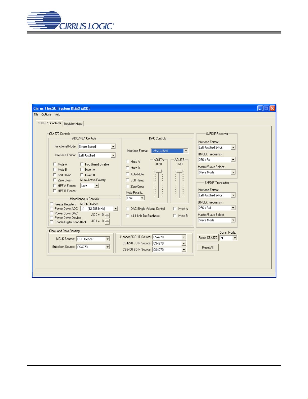
3.2 CDB4270 GUI
Brief descriptions of the GUI tab views are provided below.
The CDB4270 Controls tab provides high-level control of the CS4270, FPGA (Board Controls) and S/PDIF
Tx and Rx devices. The “CS4270 Controls” group affects that device’s register settings. The “Board Controls” group allows the user to select MCLK and sub-clock source/routing as well as CS4270 and CS8406
SDIN sources. The “S/PDIF Receiver” and “S/PDIF Transmitter” control gr oups allow the user to select data
formats, MCLK frequency and master or slave for each device. Reset push-buttons are also availa ble along
with a “Comm Mode” select drop box for CS4270 communication mode format selection.
CDB4270
Figure 7. CDB4270 Controls Tab
14 DS686DB3
Page 15
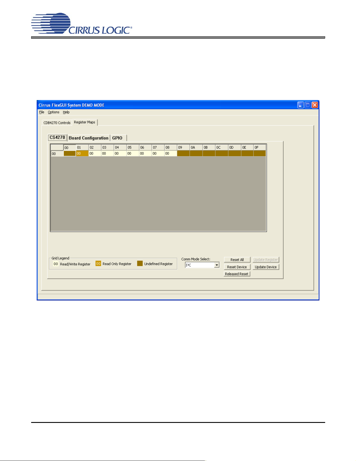
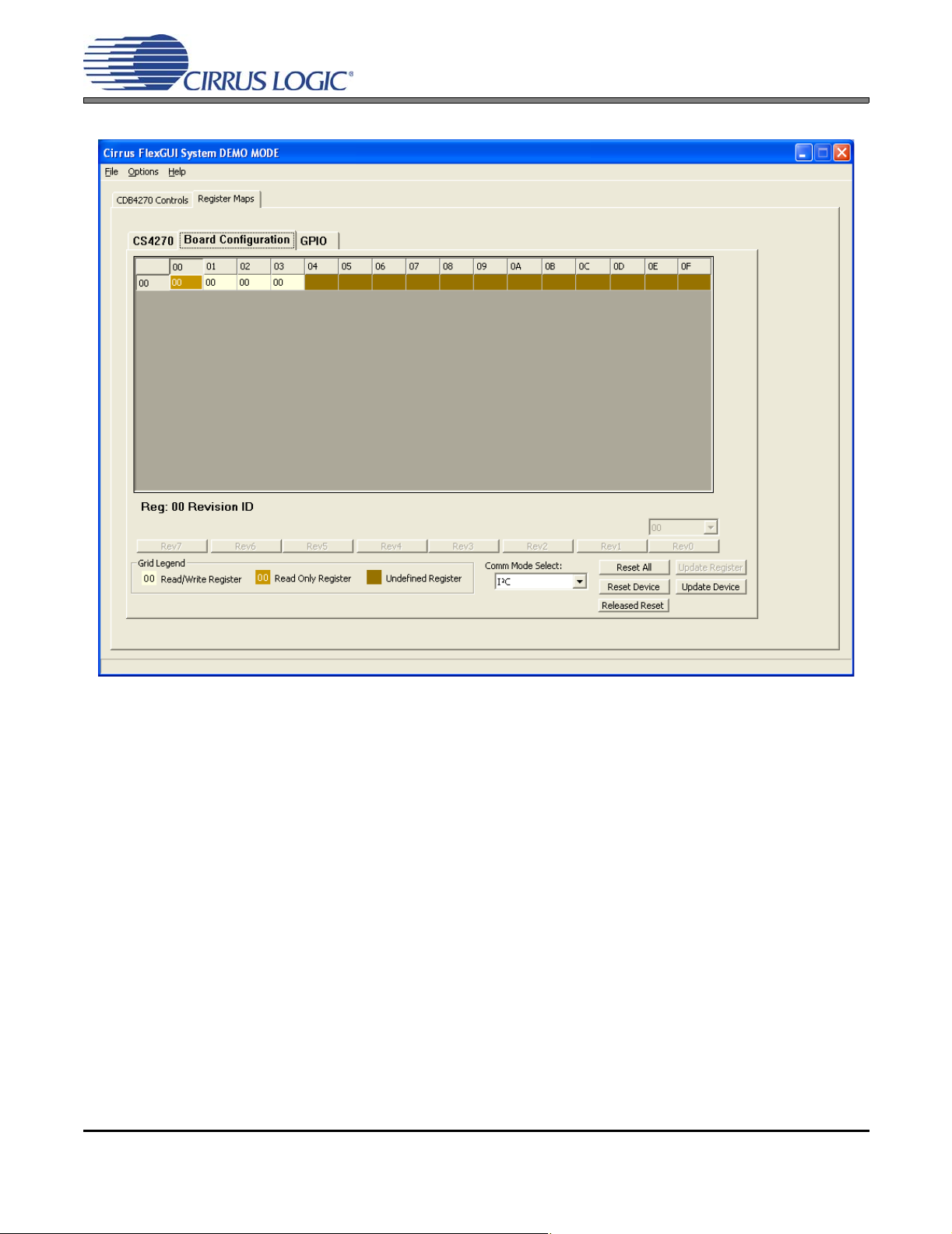
3.3 Register Maps Control Tabs
Under this tab are the CS4270, Board Configuration (FPGA) and GPIO tabs. On each tab, register values
can be modified bit-wise or byte-wise. For bit-wise modification, click the appropriate push-button fo r the
desired bit. For byte-wise modification, the desired hex value can be typed directly into th e register address
box in the register map. Refer to the CS4270 device data sheet registe r settings section and the FPGA register information in this document for register definitions.
CDB4270
Figure 8. Register Maps Tab - CS4270
DS686DB3 15
Page 16
CDB4270
Figure 9. Register Maps Tab - Board Configuration
16 DS686DB3
Page 17

CDB4270
Figure 10. Register Maps Tab - GPIO
DS686DB3 17
Page 18

CDB4270
4. HARDWARE MODE
When the Flex GUI is not running on a PC or when the USB or serial port cables are not conn ected to the CDB4270
from the PC, the board is automa tically in Hardware Control Mode. When in this control mode, dip switches S1 and
S2 control the board’s functionality. Note: Hardware Mode controls are a subset o f Software Mode controls, and
some FPGA or CS4270 register bits cannot be changed in Hardware Mode. See “CDB4270 Hardware Mode Set-
tings” on page 24 of this document for a complete description of the Hardware Mode settings.
5. FPGA GUI REGISTER DESCRIPTION
As mentioned previously, the CS4270 and FPGA registers are directly accessible in Software Mode within the Flex
GUI. In Hardware Mode, the FPGA registers control all board functions. The FPGA register descriptions for both
modes are described below. For a description of the CS4270 registers, see the CS4270 data sheet.
5.1 FPGA REGISTER QUICK REFERENCE
The table below shows the register names and their associated default values.
AddrFunction765432 1 0
Code Rev. ID
00h
SDIO/CLK/SW/HW
01h
Control
CS8406 Control
02h
CS8416 Control
03h
REV.7 REV.6 REV.5 REV.4 REV.3 REV.2 REV.1 REV.0
000101 1 1
SDIO.1 SDIO.0 Reserved MCLK DUT_SDIO.1 DUT_SDIO.0 SUB_CK.1 SUB_CK.0
000100 0 0
TXCLK.1 TXCLK.0 Reserved TX_M/S TX_FMT Reserved TXSDIO.1 TXSDIO.0
000000 0 1
Reserved RXCLK Reserved RX_M/S RX_FMT Reserved Reserved Reserved
000000 0 0
Note: Default “power on” bit states are shown.
18 DS686DB3
Page 19

CDB4270
5.2 FPGA CODE REVISION ID - ADDRESS 00H
76543210
REV.7 REV.6 REV .5 REV.4 REV.3 REV.2 REV.1 REV.0
5.2.1 Revision Number Bits (Bits 7:0)
Function:
Identifies FPGA code revision number. REV.7 - REV.4 indicate revision whole number, and REV.3 -
REV.0 indicate revision decimal number. These register bits are Read-Only. See Table 1.
REV.7 REV.6 REV.5 REV.4 REV.3 REV.2 REV.1 REV.0 Revision Number
00000000 Not Used
00010001 Revision 1.1
00010010 Revision 1.2
00010011 Revision 1.3
00010100 Revision 1.4
00010101 Revision 1.5
0001.0110 Revision 1.6
00010111 Revision 1.7
0 0 0 ... ... ... ... ... ...
00011111 Revision 1.15
... ... ... ... ... ... ... ... ...
11111001 Revision 15.9
11111010 Revision 15.10
11111011 Revision 15.11
11111100 Revision 15.12
11111101 Revision 15.13
11111110 Revision 15.14
11111111 Revision 15.15
T able 1. Revision Number
DS686DB3 19
Page 20

CDB4270
5.3 CS4270 CONTROL - ADDRESS 01H
76543210
SDIO.1 SDIO.0 Reserved MCLK DUT_SDIO.1 DUT_SDIO.0 SUB_CK.1 SUB_CK.0
5.3.1 SDOUT Routing to Header (Bits 7:6)
Default = 00
Function:
These bits control the routing of SDOUT from the CS8416, CS4270 and the Header SDIN to the Header
SDOUT. Table 2 shows the available settings.
SDIO.1 SDIO.0 SDIN/SDOUT Routing
0 0 CS4270 SDOUT source to DSP Header SDOUT
0 1 CS8416 SDOUT source to DSP Header SDOUT
1 0 SDIN from DSP Header to DSP Header SDOUT
1 1 Connect GND to DSP Header SDOUT
Table 2. SDOUT Routing to Header
5.3.2 MCLK Source (Bit 4)
Default = 1
Function:
This bit selects the source of the CS4270 MCLK signal. Table 3 shows the available settings.
MCLK MCLK Source
0 MCLK from DSP Header
1 MCLK from Oscillator (through CS8416), MCLK to DSP Header
5.3.3 SDOUT Routing to DUT (Bits 3:2)
Default = 00
Function:
These bits control the routing of SDOUT from the CS8416, CS4270 and the Header SDIN to the CS4270.
Table 4 shows the available settings
DUT_SDIO.1 DUT_SDIO.0 SDIN/SDOUT Routing
0 0 CS4270 SDOUT source to CS4270 SDIN
0 1 CS8416 SDOUT source to CS4270 SDIN
1 0 SDIN from DSP Header to CS4270 SDIN
1 1 Connect GND to CS4270 SDIN
.
Table 4. SDOUT Routing to DUT
Table 3. MCLK Source
20 DS686DB3
Page 21

5.3.4 Subclock Routing (Bits 1:0)
Default = 00
Function:
These bits select SCLK and LRCK routing to/from the CS4270, CS8416, CS8406 and the Header. Table 5
shows the available settings
SUB_CK.1 SUB_CK.0 Sub-Clock Routing
00
01
10
11
.
CDB4270
- CS4270 is Master
- CS8416 and CS8406 are Slaves to CS4270
- DSP Header Sub-clocks are Outputs from CS4270
- CS4270 and CS8406 are Slaves to CS8416
- CS8416 is Master
- DSP Header Sub-clocks are Outputs from CS8416
- CS4270 is Slave to DSP Header
- CS8416 and CS8406 are Slaves to DSP Header
- DSP Header sub clocks are Inputs
- CS4270 and CS8416 are Slave to CS8406
- CS8406 is Master
- DSP Header Sub-clocks are Outputs from CS8406
Table 5. Sub-Clock Routing
5.4 CS8406 TX CONTROL - ADDRESS 02H
76543210
TXCLK.1 TXCLK.0 Reserved TX_M/S TX_FMT Reserved TXSDIO.1 TXSDIO.0
5.4.1 CS8406 OMCLK Divider Control (Bits 7:6)
Default = 00
Function:
These bits select the CS8406 OMCLK divider ratio. Table 6 shows the available settings.
TXCLK.1 TXCLK.0 CS8406 OMCLK Frequency
0 0 256 x Fs
0 1 128 x Fs
1 0 512 x Fs
1 1 256 x Fs
Table 6. CS8406 OMCLK Frequency
DS686DB3 21
Page 22

5.4.2 CS8406 Master/Slave Select (Bit 4)
Default = 0
Function:
This bit selects CS8406 Master Mode (SCLK, LRCK are outputs) or Slave Mode (SCLK, LRCK are inputs). See Table 7.
TX_M/S CS8406 Master/Slave
0 CS8406 Slave Mode
1 CS8406 Master Mode
Table 7. CS8406 Master/Slave
5.4.3 CS8406 SDIN Format Select (Bit 3)
Default = 0
Function:
This bit selects the CS8406 SDIN format. See Table 8.
TX_FMT CS8406 SDIN Format
0 24-bit Left-Justified
1 24-bit I²S
Table 8. CS8406 SDIN Format
CDB4270
5.4.4 CS8406 SDIN Source (Bits 1:0)
Default = 01
Function:
These bits select the source of the CS8406 SDIN Signal. Table 9 shows the available settings.
TXSDIO.1 TXSDIO.0 CS8406 SDIN Source
0 0 CS4270 SDOUT
0 1 CS8416 SDOUT
1 0 SDIN from Header
11 GND
Table 9. CS8406 SDIN Source
22 DS686DB3
Page 23

CDB4270
5.5 CS8416 RX CONTROL - ADDRESS 03H
76543210
Reserved RXCLK Reserved RX_M/S RX_FMT Reserved Reserved Reserved
5.5.1 CS8416 RMCLK Divider Control (Bit 6)
Default = 0
Function:
This bit selects the CS8416 RMCLK divider ratio. Table 10.
RXCLK CS8416 RMCLK Frequency
0 256 x Fs
1 128 x Fs
T able 10. CS8416 RMCLK Frequency
5.5.2 CS8416 Master/Slave Select (Bit 4)
Default = 0
Function:
This bit selects CS8416 Master Mode (SCLK, LRCK are ou tputs) or Slave Mode (SCLK, LRCK are inputs). See Table 11
RX_M/S CS8416 Master/Slave
0 CS8416 Slave Mode
1 CS8416 Master Mode
Table 11. CS8416 Master/Slave
5.5.3 CS8416 SDOUT Format Select (Bit 3)
Default = 0
Function:
This bit selects the CS8416 SDOUT format. See.Table 12
RX_FMT CS8416 SDOUT Format
0 24-bit Left-Justified
1 24-bit I²S
Table 12. CS8416 SDOUT Format
DS686DB3 23
Page 24

CDB4270
6. CDB4270 HARDWARE MODE SETTINGS
Schematic-Level Functional Description:
When the Flex GUI is not used and there is no serial p ort commu nication to the board, all devices ar e in HW Mode.
FPGA SW control is disabled in this condition, and DIP switches S1 and S2 on the CDB4270 set the FPGA Registers
to control board functionality. Note that the CS8406 and CS8416 are reset when SW/HW
goes low (going from SW to HW Mode). See the schematic for switch name labels, and see Table 13.
Dip Switch
S1 0,0
S1 0,1
S1 1,0
S1 1,1
Dip Switch
S1 0,0
S1 0,1
S1 1,0
S1 1,1
Dip Switch
S1 0
S1 1
Logic State
b1, b0 nets
Logic State
b3, b2 nets
Logic State
b4 nets
Table 13. CDB4270 Hardware Mode - Functional Description
Functional Description
As per Table 5.
- CS4270 is Master
- CS8416 and CS8406 are Slaves to CS4270
- DSP Header Sub-clocks are Outputs from CS4270
As per Table 5.
- CS8416 is Master
- CS4270 and CS8406 are Slaves to CS8416
- DSP Header Sub-clocks are Outputs from CS8416
As per Table 5.
-DSP Header is Master
- CS4270, CS8416 and CS8406 are Slaves to DSP Header
- DSP Header Sub-clocks are Inputs
As per Table 5.
- CS8406 is Master
- CS4270 and CS8416 are Slave to CS8406
- DSP Header Sub-clocks are Outputs from CS8406
Functional Description
As per Table 2, Table 4, Table 9.
CS4270 SDOUT to DSP Header SDOUT
CS4270 SDOUT to CS4270 SDIN
CS4270 SDOUT to CS8406 SDIN
As per Table 2, Table 4, Table 9.
CS8416 SDOUT to DSP Header SDOUT
CS8416 SDOUT to CS4270 SDIN
CS8416 SDOUT to CS8406 SDIN
As per Table 2, Table 4, Table 9.
DSP Header SDIN to DSP Header SDOUT
DSP Header SDIN to CS4270 SDIN
DSP Header SDIN to CS8406 SDIN
As per Table 2, Table 4, Table 9.
DSP Header SDIN to DSP Header SDOUT
DSP Header SDIN to CS4270 SDIN
DSP Header SDIN to CS8406 SDIN
FPGA Functional Description
As per Table 3.
MCLK from DSP Header
As per Table 3.
MCLK from Oscillator (through CS8416), MCLK to DSP Header
from the microprocessor
24 DS686DB3
Page 25

Dip Switch
S2 0,0,0,0
S2 0,1,0,0
S2 1,0,0,0
S2 1,0,1,0
S2 1,1,10
S2 1,1,1,1
Dip Switch
S2 0
S2 1
(1) Logic State
M1, M0, MDIV2,
MDIV1
Logic State
DIF net
CDB4270
CS4270 Functional
Sets CS4270 Single Speed MCLK divide by 1 Mode, no de-emphasis, CS8406
OMCLK=256xFs and CS8416 RMCLK=256xFs
Sets CS4270 Single Speed MCLK divide by 1 Mode, w/de-emphasis, CS8406
OMCLK=256xFs and CS8416 RMCLK=256xFs
Sets CS4270 Double Speed MCLK divide by 1 Mode, no de-emphasis, CS8406
OMCLK=128xFs and CS8416 RMCLK=128xFs
Sets CS4270 Double Speed MCLK divide by 2 Mode, no de-emphasis, CS8406
OMCLK=256xFs and CS8416 RMCLK=256xFs
Sets CS4270 Quad Speed MCLK divide by 2 Mode, no de-emphasis, CS8406
OMCLK=128xFs and CS8416 RMCLK=128xFs
Sets CS4270 Quad Speed MCLK divide by 4 Mode, no de-emphasis, CS8406
OMCLK=256xFs and CS8416 RMCLK=256xFs
CS4270 Functional Description
Sets CS4270 24-bit LJ Mode for SDIN and SDOUT. CS8406 set to LJ Mode for SDIN
and CS8416 set to LJ Mode for serial data
Sets CS4270 24-bit I²S Mode for SDIN and SDOUT. CS8406 set to I²S Mode for
SDIN and CS8416 set to I²S Mode for serial data
Table 13. CDB4270 Hardware Mode - Functional Description
1. For other M1, M0, MDIV2, MDIV1 states, CS8406 OMCLK=256xFs and CS8416 RMCLK=256xFs.
Note: Whenever changes are made to the S/PDIF Receiver (CS8416), the FPGA (for CS4270 HW or SW
Modes) generates a CS8416.RESET
shows the parameters that apply. Also, whenever CS4270-M/S
FPGA generates a HDR-RESET
(CS8416 RESET) after the parameter is changed. Reg 03h (FPGA)
(CS4270 master/slave) changes state, the
(CS4270 RESET).
DS686DB3 25
Page 26

7. CDB CONNECTORS, SWITCHES, INDICATORS AND JUMPERS
CDB4270
CONNECTOR,
SWITCH
+5V J1 Input +5.0 V Power Supply
CLK/DATA CON-
TROL
HW MODE CONFIG S2 Input HW Mode CS4270 Mode Control Switch
GND J2 Input Ground Reference
SPDIF OPTICAL
OUT
SPDIF COAX OUT J7 Output CS8406 digital audio output via coaxial cable
SPDIF OPTICAL IN OPT1 Input CS8416 digital audio input via optical cable
SPDIF COAX IN J5 Input CS8416 digital audio input via coaxial cable
RS232 J16 Input/Output
USB J15 Input/Output
DSP HEADER J9 Input/Output I/O for Clocks & Data
SERIAL CONTROL J10 Input/Output
MICRO C2 HEADER J14 Input/Output I/O for programming the micro controller (U21)
FPGA JTAG J12 Input/Output I/O for programming the FPGA (U11)
MICRO RESET S4 Input Reset for the micro controller (U21)
AINA
AINB
AOUTA
AOUTB
JUMPER/
INDICATOR
CONTROL
JUMPERS
MUTEA
JUMPERS
MUTEB
JUMPERS
MUTEA LED
MUTEB LED
INIT
INDICATOR Indicates FPGA program INIT D5 FPGA is being programmed when on
DONE Indicates FPGA program complete D4 FPGA has been programmed when on
RCVR ERROR Indicates CS8416 Data Receive Error D2 Indicates Data Receive Error when on
USB PRESENT Indicates USB Connection D7 Indicates USB connection when on
Reference
Designator INP UT/OUTPUT SIGNAL PRESENT
S1 Input HW Mode Clock/Data Routing Control Dip Switch
OPT2 Output CS8406 digital audio output via optical cable
Serial connection to PC for SPI / I²C Control Port signals
USB connection to PC for SPI /
I/O for external SPI /
J13
J11
J6
J4
Input RCA phono jacks for analog inputs
Output RCA phono jacks for analog outputs
T able 14. Connectors and Switches
PURPOSE
SPI/I²C control Internal or external select
Selects between MUTEA
MUTEA LED Indicator Enable
Selects between MUTEB
MUTEB LED Indicator Enable
Indicates that CS4270 MUTEA
present
Indicates that CS4270 MUTEB
present
Enable and
Enable and
signal is
signal is
Table 15. Jumpers and Indicators
POSITION/
REF DES
*J10, pins 1-2
J10, none
*J8, pins 1-2
J8, pins 2-3
*J3, pins 1-2
J3, pins 2-3
D3
D1
I²C Control Port signals
MUTEA
MUTEB
I²C Control Port signals
FUNCTION SELECTED/INDICATION
*Normal I²C/SPI Operation
Connect to pins 2 (control) and 3 (gnd) for
external control
* MUTEA
MUTEA LED Enable
* MUTEB
MUTEB LED Enable
from CS4270 is present when LED
from CS4270 is present when LED
Enable
Enable
is on
is on
*Default factory settings
26 DS686DB3
Page 27
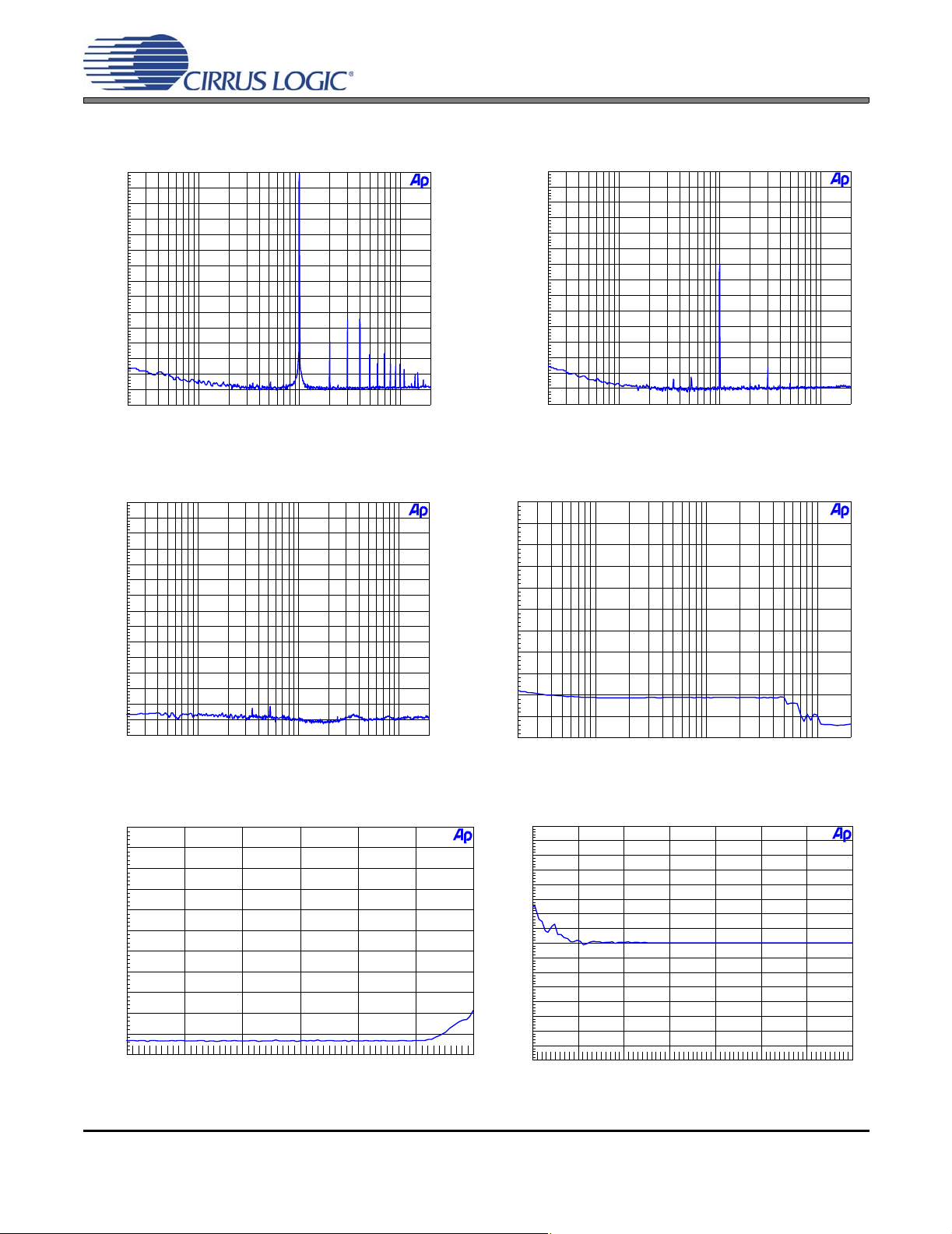
8. ADC PERFORMANCE PLOTS
CDB4270
+0
-10
-20
-30
-40
-50
-60
d
-70
B
F
-80
S
-90
-100
-110
-120
-130
-140
-150
20 20k50 100 200 500 1k 2k 5k 10k
Hz
Figure 11. FFT (-1 dB 48 kHz) Figure 12. FFT (-60 dB, 48 kHz)
+0
-10
-20
-30
-40
-50
-60
d
-70
B
F
-80
S
-90
-100
-110
-120
-130
-140
-150
20 20k50 100 200 500 1k 2k 5k 10k
Hz
Figure 13. FFT (48 kHz, No Input) Figure 14. 48 kHz, THD+N vs. Input Freq
+0
-10
-20
-30
-40
-50
-60
d
-70
B
F
-80
S
-90
-100
-110
-120
-130
-140
-150
20 20k50 100 200 500 1k 2k 5k 10k
+0
-10
-20
-30
-40
d
-50
B
F
-60
S
-70
-80
-90
-100
-110
20 20k50 100 200 500 1k 2k 5k 10k
Hz
Hz
+0
-10
-20
-30
-40
d
-50
B
F
-60
S
-70
-80
-90
-100
-110
-120 +0-100 -80 -60 -40 -20
dBr
+40
+35
+30
+25
+20
+15
+10
+5
d
B
+0
F
S
-10
-15
-20
-25
-30
-35
-40
TTTTT
-5
-140 +0-120 -100 -80 -60 -40 -20
dBr
Figure 15. 48 kHz, THD+N vs. Level Figure 16. 48 kHz, Fade-to-Noise Linearity
DS686DB3 27
Page 28

CDB4270
+5
+4
+3
+2
+1
d
B
+0
F
S
-1
-2
-3
-4
-5
20 20k50 100 200 500 1k 2k 5k 10k
Hz
+0
-10
-20
-30
-40
-50
-60
d
-70
B
F
-80
S
-90
-100
-110
-120
-130
-140
-150
20 20k50 100 200 500 1k 2k 5k 10k
Hz
Figure 17. 48 kHz, Frequency Response Figure 18. 48 kHz, Crosstalk
+0
-10
-20
-30
-40
-50
-60
d
-70
B
F
-80
S
-90
-100
-110
-120
-130
-140
-150
20 20k50 100 200 500 1k 2k 5k 10k
Hz
+0
-10
-20
-30
-40
-50
-60
d
-70
B
F
-80
S
-90
-100
-110
-120
-130
-140
-150
20 20k50 100 200 500 1k 2k 5k 10k
Hz
Figure 19. FFT (-1 dB 96 kHz) Figure 20. FFT (-60 dB, 96 kHz)
+0
-10
-20
-30
-40
-50
-60
d
-70
B
F
-80
S
-90
-100
-110
-120
-130
-140
-150
20 20k50 100 200 500 1k 2k 5k 10k
Hz
+0
-10
-20
-30
-40
d
-50
B
F
-60
S
-70
-80
-90
-100
-110
20 20k50 100 200 500 1k 2k 5k 10k
Hz
Figure 21. FFT (96 kHz, No Input) Figure 22. 96 kHz, THD+N vs. Input Freq
28 DS686DB3
Page 29

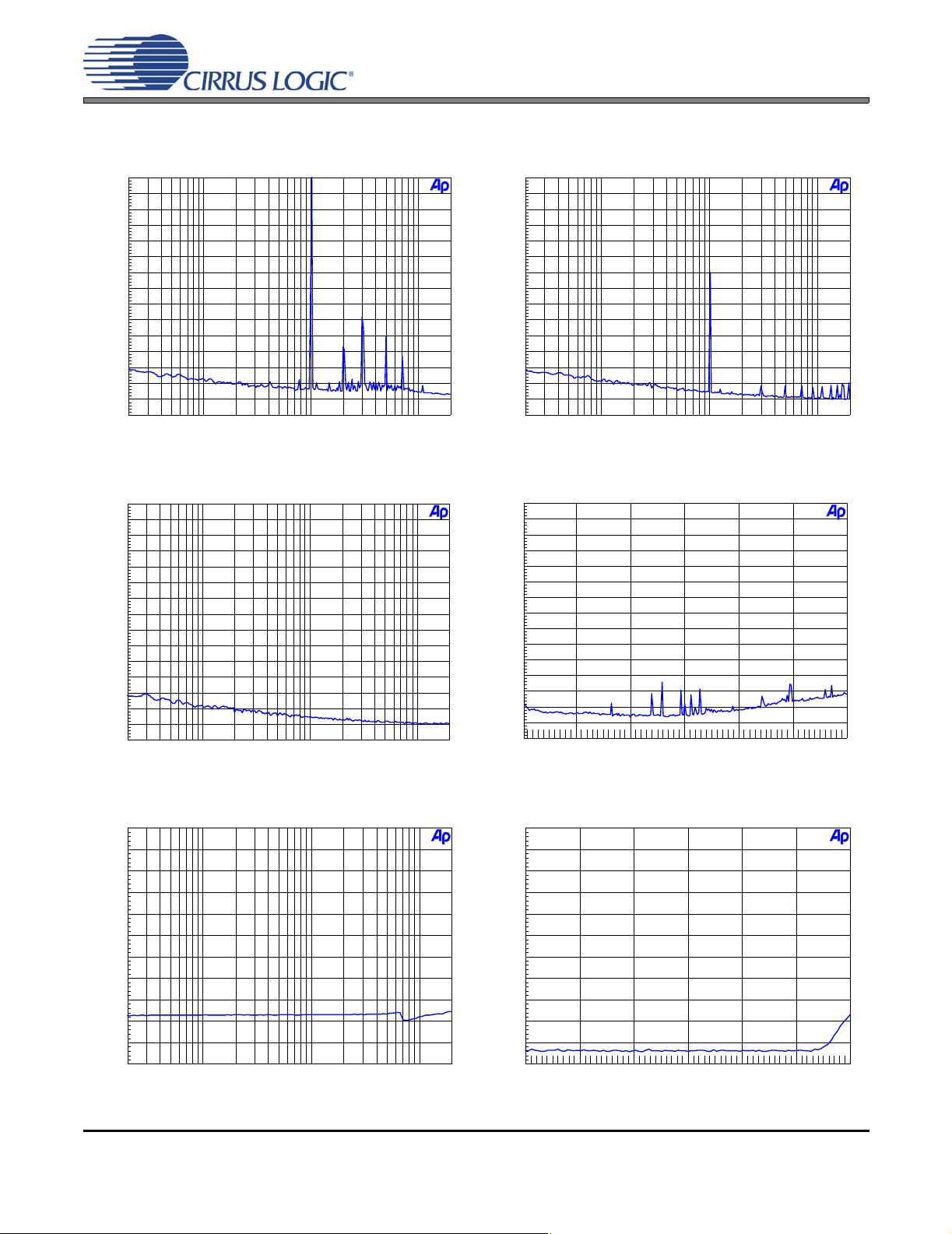
CDB4270
+0
-10
-20
-30
-40
d
-50
B
F
-60
S
-70
-80
-90
-100
-110
-120 +0-100 -80 -60 -40 -20
dBr
Figure 23. 96 kHz, THD+N vs. Level Figure 24. 96 kHz, Fade-to-Noise Linearity
+5
+4
+3
+2
+1
d
B
+0
F
S
-1
-2
-3
-4
-5
20 20k50 100 200 500 1k 2k 5k 10k
Hz
+40
TTT
+35
+30
+25
+20
+15
+10
+5
d
B
+0
F
S
-5
-10
-15
-20
-25
-30
-35
-40
-140 +0-120 -100 -80 -60 -40 -20
+0
-10
-20
-30
-40
-50
-60
d
-70
B
F
-80
S
-90
-100
-110
-120
-130
-140
-150
20 20k50 100 200 500 1k 2k 5k 10k
dBr
Hz
Figure 25. 96 kHz, Frequency Response Figure 26. 96 kHz, Crosstalk
+0
-10
-20
-30
-40
-50
-60
d
-70
B
F
-80
S
-90
-100
-110
-120
-130
-140
-150
20 20k50 100 200 500 1k 2k 5k 10k
Hz
+0
-10
-20
-30
-40
-50
-60
d
-70
B
F
-80
S
-90
-100
-110
-120
-130
-140
-150
20 20k50 100 200 500 1k 2k 5k 10k
Hz
Figure 27. FFT (-1 dB 192 kHz) Figure 28. FFT (192 kHz, -60 dB)
DS686DB3 29
Page 30

CDB4270
+0
-10
-20
-30
-40
-50
-60
d
-70
B
F
-80
S
-90
-100
-110
-120
-130
-140
-150
20 20k50 100 200 500 1k 2k 5k 10k
Hz
Figure 29. FFT (192 kHz, No Input) Figure 30. 192 kHz, THD+N vs. Input Freq
+0
-10
-20
-30
-40
d
-50
B
F
-60
S
-70
-80
-90
-100
-110
-120 +0-100 -80 -60 -40 -20
dBr
+0
-10
-20
-30
-40
d
-50
B
F
-60
S
-70
-80
-90
-100
-110
20 20k50 100 200 500 1k 2k 5k 10k
+40
TTTTTT
+35
+30
+25
+20
+15
+10
+5
d
B
+0
F
S
-5
-10
-15
-20
-25
-30
-35
-40
-140 +0-120 -100 -80 -60 -40 -20
Hz
dBr
Figure 31. 192 kHz, THD+N vs. Level Figure 32. 192 kHz, Fade-to-Noise Linearity
+5
+4
+3
+2
+1
d
B
+0
F
S
-1
-2
-3
-4
-5
20 20k50 100 200 500 1k 2k 5k 10k
Hz
+0
-10
-20
-30
-40
-50
-60
d
-70
B
F
-80
S
-90
-100
-110
-120
-130
-140
-150
20 20k50 100 200 500 1k 2k 5k 10k
Hz
Figure 33. 192 kHz, Frequency Response Figure 34. 192 kHz, Crosstalk
30 DS686DB3
Page 31
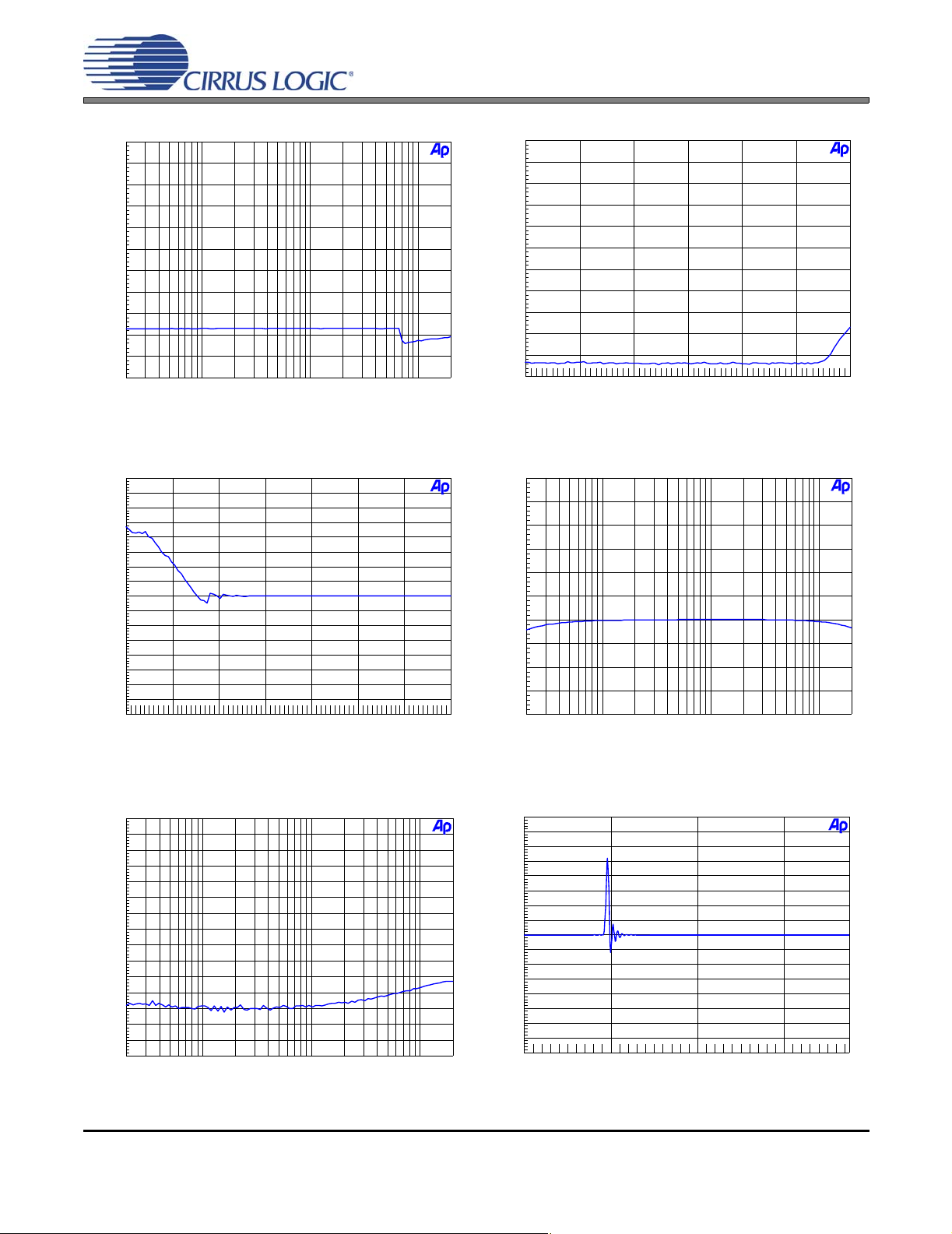
9. DAC PERFORMANCE PLOTS
CDB4270
+0
-10
-20
-30
-40
-50
-60
d
-70
B
r
-80
A
-90
-100
-110
-120
-130
-140
-150
20 20k50 100 200 500 1k 2k 5k 10k
Hz
Figure 35. FFT (48 kHz, 0 dB) Figure 36. FFT (48 kHz, -60 dB)
+0
-10
-20
-30
-40
-50
-60
d
-70
B
r
-80
A
-90
-100
-110
-120
-130
-140
-150
20 20k50 100 200 500 1k 2k 5k 10k
Hz
Figure 37. FFT (48 kHz, No Input) Figure 38. FFT (48 kHz Out-of-Band, No Input)
+0
-10
-20
-30
-40
-50
-60
d
-70
B
r
-80
A
-90
-100
-110
-120
-130
-140
-150
20 20k50 100 200 500 1k 2k 5k 10k
+0
-10
-20
-30
-40
-50
-60
d
-70
B
r
-80
A
-90
-100
-110
-120
-130
-140
-150
20k 120k40k 60k 80k 100k
Hz
Hz
+0
-10
-20
-30
-40
d
-50
B
r
-60
A
-70
-80
-90
-100
-110
20 20k50 100 200 500 1k 2k 5k 10k
Hz
+0
-10
-20
-30
-40
d
-50
B
r
-60
A
-70
-80
-90
-100
-110
-120 +0-100 -80 -60 -40 -20
dBFS
Figure 39. 48 kHz, THD+N vs. Input Freq Figure 40. 48 kHz, THD+N vs. Level
DS686DB3 31
Page 32

CDB4270
+40
+35
+30
+25
+20
+15
+10
d
+5
B
+0
r
-5
A
-10
-15
-20
-25
-30
-35
-40
-140 +0-120 -100 -80 -60 -40 -20
dBFS
+5
+4
+3
+2
+1
d
B
+0
r
A
-1
-2
-3
-4
-5
20 20k50 100 200 500 1k 2k 5k 10k
Hz
Figure 41. 48 kHz, Fade-to-Noise Linearity Figure 42. 48 kHz, Frequency Response
+0
T TTTTTTTTTT TT TT TTTT TTT TTT TTTT TT T T TT
-10
-20
-30
-40
-50
-60
d
-70
B
r
-80
A
-90
-100
-110
-120
-130
-140
-150
20 20k50 100 200 500 1k 2k 5k 10k
Hz
2
1.75
1.5
1.25
1
750m
500m
250m
0
V
-250m
-500m
-750m
-1
-1.25
-1.5
-1.75
-2
0 3m500u 1m 1.5m 2m 2.5m
sec
Figure 43. 48 kHz, Crosstalk Figure 44. 48 kHz, Impulse Response
+0
-10
-20
-30
-40
-50
-60
d
-70
B
r
-80
A
-90
-100
-110
-120
-130
-140
-150
20 20k50 100 200 500 1k 2k 5k 10k
Hz
+0
-10
-20
-30
-40
-50
-60
d
B
-70
r
-80
A
-90
-100
-110
-120
-130
-140
-150
20 20k50 100 200 500 1k 2k 5k 10k
Hz
Figure 45. FFT (96 kHz, 0 dB) Figure 46. FFT (96 kHz, -60 dB)
32 DS686DB3
Page 33

CDB4270
+0
-10
-20
-30
-40
-50
-60
d
B
-70
r
-80
A
-90
-100
-110
-120
-130
-140
-150
20 20k50 100 200 500 1k 2k 5k 10k
Hz
Figure 47. FFT (96 kHz, No Input) Figure 48. FFT (96 kHz Out-of-Band, No Input)
+0
-10
-20
-30
-40
d
-50
B
r
-60
A
-70
-80
-90
-100
-110
20 20k50 100 200 500 1k 2k 5k 10k
Hz
+0
-10
-20
-30
-40
-50
-60
d
B
-70
r
-80
A
-90
-100
-110
-120
-130
-140
-150
+0
-10
-20
-30
-40
d
-50
B
r
-60
A
-70
-80
-90
-100
-110
-120 +0-100 -80 -60 -40 -20
20k 120k40k 60k 80k 100k
Hz
dBFS
Figure 49. 96 kHz, THD+N vs. Input Freq Figure 50. 96 kHz, THD+N vs. Level
+40
+35
+30
+25
+20
+15
+10
d
+5
B
+0
r
-5
A
-10
-15
-20
-25
-30
-35
-40
-140 +0-120 -100 -80 -60 -40 -20
dBFS
+5
+4
+3
+2
+1
d
B
+0
r
A
-1
-2
-3
-4
-5
20 20k50 100 200 500 1k 2k 5k 10k
Hz
Figure 51. 96 kHz, Fade-to-Noise Linearity Figure 52. 96 kHz, Frequency Response
DS686DB3 33
Page 34

CDB4270
+0
TTT T TTT T TT T TT TTTTTTT TTTT TTTTTT TTT
-10
-20
-30
-40
-50
-60
d
B
-70
r
-80
A
-90
-100
-110
-120
-130
-140
-150
20 20k50 100 200 500 1k 2k 5k 10k
Hz
Figure 53. 96 kHz, Crosstalk Figure 54. 96 kHz, Impulse Response
+0
-10
-20
-30
-40
-50
-60
d
B
-70
r
-80
A
-90
-100
-110
-120
-130
-140
-150
20 20k50 100 200 500 1k 2k 5k 10k
Hz
2
1.75
1.5
1.25
1
750m
500m
250m
0
V
-250m
-500m
-750m
-1
-1.25
-1.5
-1.75
-2
0 1.5m250u 500u 750u 1m 1.25m
+0
-10
-20
-30
-40
-50
-60
d
B
-70
r
-80
A
-90
-100
-110
-120
-130
-140
-150
20 20k50 100 200 500 1k 2k 5k 10k
sec
Hz
Figure 55. FFT (192 kHz, 0 dB) Figure 56. FFT (192 kHz, -60 dB)
+0
-10
-20
-30
-40
-50
-60
d
B
-70
r
-80
A
-90
-100
-110
-120
-130
-140
-150
20 20k50 100 200 500 1k 2k 5k 10k
Hz
+0
-10
-20
-30
-40
-50
-60
d
B
-70
r
-80
A
-90
-100
-110
-120
-130
-140
-150
20k 120k40k 60k 80k 100k
Hz
Figure 57. FFT (192 kHz, No Input) Figure 58. FFT (192 kHz Out-of-Band, No Input)
34 DS686DB3
Page 35
CDB4270
+0
-10
-20
-30
-40
d
-50
B
r
-60
A
-70
-80
-90
-100
-110
20 20k50 100 200 500 1k 2k 5k 10k
Hz
+0
-10
-20
-30
-40
d
-50
B
r
-60
A
-70
-80
-90
-100
-110
-120 +0-100 -80 -60 -40 -20
dBFS
Figure 59. 192 kHz, THD+N vs. Input Freq Figure 60. 192 kHz, THD+N vs. Level
+40
+35
+30
+25
+20
+15
+10
d
+5
B
+0
r
-5
A
-10
-15
-20
-25
-30
-35
-40
-140 +0-120 -100 -80 -60 -40 -20
dBFS
+5
+4
+3
+2
+1
d
B
+0
r
A
-1
-2
-3
-4
-5
20 20k50 100 200 500 1k 2k 5k 10k
Hz
Figure 61. 192 kHz, Fade-to-Noise Linearity Figure 62. 192 kHz, Frequency Response
+0
TTTTTTTTTTTTTTTT T TTT TTTTTTTTTTTTTTT
-10
-20
-30
-40
-50
-60
d
-70
B
r
-80
A
-90
-100
-110
-120
-130
-140
-150
20 20k50 100 200 500 1k 2k 5k 10k
Hz
2
1.75
1.5
1.25
1
750m
500m
250m
0
V
-250m
-500m
-750m
-1
-1.25
-1.5
-1.75
-2
0 600u200u 400u
sec
Figure 63. 192 kHz, Crosstalk Figure 64. 192 kHz, Impulse Response
DS686DB3 35
Page 36
36 DS686DB3
10.CDB BLOCK DIAGRAM
CS8406
S/PDIF
Output
Figure 19
CS8416
S/PDIF
Input
Figure 20
Osc.
Clocks/Data
Hardware
Setup
Clocks
/Data
Hardware
Setup
MCLK BUS
FPGA
Figure 22
Figure 23
ADC/DAC
Clocks/
Data
Hardware
Setup
USB/Serial Control Port
I2C/SPI Header
CS4270
Figure 16
HW Setup
Switches
Figure 22
Power
Figure 24
ANALOG INPUT
Figure 23
Single-Ended Input
Figure 17
ANALOG OUTPUT
Single-Ended
Output
Figure 18
Figure 21
ADC/DAC Clocks & Data
DSP HEADER
Figure 21
CDB4270
Figure 65. Block Diagram
Page 37

DS686DB3 37
11.CDB SCHEMATICS
Figure 66. CS4270
CDB4270
Page 38

38 DS686DB3
Figure 67. Analog Input
CDB4270
Page 39

DS686DB3 39
Figure 68. Analog Output
CDB4270
Page 40

40 DS686DB3
Figure 69. CS8406 S/PDIF Transmitter
CDB4270
Page 41

DS686DB3 41
Figure 70. CS8416 S/PDIF Receiver
CDB4270
Page 42

42 DS686DB3
Figure 71. Buffers - Clock/Data Routing
CDB4270
Page 43
DS686DB3 43
Figure 72. FPGA
CDB4270
Page 44

44 DS686DB3
Figure 73. USB/RS232 Microprocessor
CDB4270
Page 45

DS686DB3 45
Figure 74. Power
CDB4270
Page 46

46 DS686DB3
12.CDB LAYOUT
Figure 75. Silk Screen
CDB4270
Page 47

DS686DB3 47
Figure 76. Top-Side Layer
CDB4270
Page 48

48 DS686DB3
Figure 77. Bottom-Side Layer
CDB4270
Page 49

13.CHANGES MADE TO REV. B BOARD
13.1 Modifications (Done by Cirrus Logic)
Note: There is no rework necessary when CS4270 C0 parts are installed on the Rev. B board. See CDB
Data Sheet DS686DB2 when B0 parts are installed on the Rev. B board or DS686DB1 when A0
parts are installed on the Rev. A board. Also reference the Rev. A0, B0, and C0 chip Errata at
http://www.cirrus.com/en/support. Select Errata from the product information categories shown.
CDB4270
DS686DB3 49
Page 50

14.REVISION HISTORY
Revision Changes
DB1 Initial Release: Applies to A Assy. (A2 PL).
This Revision is for the B Assy. (B2 PL). Updates for USB port use, new GUI graphics, new schematics, new
DB2
DB3
rework information, new layout graphics and added performance plots. Removed Rev. A/A1 (PL) references,
schematics, layout graphics and rework.
Added Performance Plots
Replaced Figure 67 on page 38
Deleted Figure 28, Board Modifications
CDB4270
Contacting Cirrus Logic Support
For all product questions and inquiries, contact a Cirrus Logic Sales Representative.
To find the one nearest you, go to www.cirrus.com.
IMPORTANT NOTICE
Cirrus Logic, Inc. and its subsidiaries ("Cirrus") believe that the information contained in this document is accurate and reliable. However, the information is subject
to change without not ice and is pr ovided "AS IS" witho ut warr anty of any kind (express or implied). Customers are advised to obtain the latest version of relevant
information to verify, before placing orders, that information being relied on is current and complete. All products are sold subject to the terms and conditions of sale
supplied at the time of order acknowledgment, including those pertaining to warranty, indemnification, and limitation of liability. No responsibility is assumed by Cirrus
for the use of this information, including use of this information as the basis for manufacture or sale of any items, or for infringement of patents or other rights of third
parties. This document is the property of Cirrus and by furnishing this information, Cirrus grants no license, express or implied under any patents, mask work rights,
copyrights, trademarks, trade secrets or other inte llectual property rig hts. Cirrus owns the copyrights associated with the information contained herein and gives consent for copies to be made of the information only for use within your organization with respect to Cirrus integrated circuits or other products of Cirrus. This consent
does not extend to other copying such as copying for general distribution, advertising or promotional purposes, or for creating any work for resale.
CERTAIN APPLICATIONS USING SEMICONDUCTOR PRODUCTS MAY INVOLVE POTENTIAL RISKS OF DEATH, PERSONAL INJURY, OR SEVERE PROPERTY OR ENVIRONMENTAL DAMAGE (“CRITICAL APPLICATIONS”). CIRRUS PRODUCTS ARE NOT DESIGNED, AUTHORIZED OR WARRANTED FOR USE
IN AIRCRAFT SYSTEMS, MILITARY APPLICATIONS, PRODUCTS SURGICALLY IMPLANTED INTO THE BODY, AUTOMOTIVE SAFETY OR SECURITY DEVICES, LIFE SUPPORT PRODUCTS OR OTHER CRITICAL APPLICATIONS. INCLUSION OF CIRRUS PRODUCTS IN SUCH APPLICATIONS IS UNDERSTOOD TO BE FULLY AT THE CUSTOMER’S RISK AND CIRRUS DISCLAIMS AND MAKES NO WARRANTY, EXPRESS, STATUTORY OR IMPLIED,
INCLUDING THE IMPLIED WARRANTIES OF MERCHANTABILITY AND FITNESS FOR PARTICULAR PURPOSE, WITH REGARD TO ANY CIRRUS PRODUCT
THAT IS USED IN SUCH A MANNER. IF THE CUSTOMER OR CUSTOMER’S CUSTOMER USES OR PERMITS THE USE OF CIRRUS PRODUCTS IN CRITICAL
APPLICATIONS, CUSTOMER AGREES, BY SUCH USE, T O FULLY INDEMNIF Y CIRRUS, ITS OF FICE RS, DI RECTORS, EMPLOYEES, DISTRI BUTORS AND
OTHER AGENTS FROM ANY AND ALL LIABILITY, INCLUDING ATTORNEYS’ FEES AND COSTS, THAT MAY RESULT FROM OR ARISE IN CONNECTION
WITH THESE USES.
Cirrus Logic, Cirrus, and the Cirrus Logic logo designs, and P opguar d are tradem arks of Cirrus Lo gic, Inc. All other bran d and product names in this document may
be trademarks or service marks of their respective owners.
I²C is a registered trademark of Philips Semiconductor.
SPI is a trademark of Motorola, Inc.
Windows
is a registered trademark of Microsoft Corporation.
50 DS686DB3
 Loading...