

Page 1
Evaluation Board for CS4245
CDB4245
Features
z Single-ended Analog Inputs
z Single-ended Analog Outputs
z CS8406 S/PDIF Digital Audio Transmitter
z CS8416 S/PDIF Digital Audio Receiver
z Independent ADC and DAC Clock Domains
z Header for Optional External Software
Configuration of CS4245
z Header for External PCM Serial Audio I/O
z 3.3 V Logic Interface
z Pre-defined Software Scripts
z Demonstrates Recommended Layout and
Grounding Arrangements
z Windows
to Configure CS4245 and Inter-board
Connections
ORDERING INFORMATION
CDB4245 Evaluation Board
®
Compatible Software Interface
Description
The CDB4245 evaluation board is an excellent means
for evaluating the CS4245 CODEC. Evaluation requires
an analog/digital signal source and analyzer, and power
supplies. A Windows
used to evaluate the CS4245.
System timing for the I²S, Left-Justified and Right-Justified interface formats can be provided by the CS4245,
the CS8416, the CS8406, or by a PCM I/O stake header
with an external source connected.
RCA phono jacks are provided for the CS4245 analog inputs and outputs. Digital data I/O is available via RCA
phono or optical connectors to the CS8416 and CS8406.
The Windows
®
uration of the CDB4245 easy. The software
communicates through the PC’s serial port to configure
the control port registers so that all features of the
CS4245 can be evaluated. The evaluation board may
also be configured to accept external timing and data
signals for operation in a user application during system
development.
®
PC compatible computer must be
software provides a GUI to make config-
I
Cirrus Logic, Inc.
www.cirrus.com
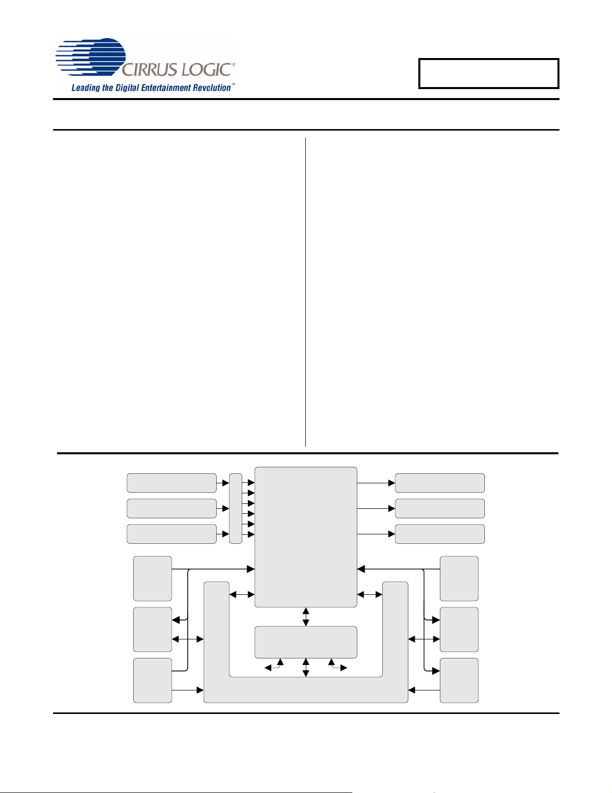
Passive Input Filter
M
Active Input Filter
Microphone Input
Master Clock Master Clock
Canned
Oscillator
Header
CS8416 CS8406
U
X
CS4245
Control Port Interface
CS8416 CS8406
FPGA
Sub-clocks and Data
Copyright © Cirrus Logic, Inc. 2005
(All Rights Reserved)
Passive Output Filter
Active Output Filter
Test Points
Canned
Oscillator
Header
FEB ‘05
DS656DB1
Page 2

TABLE OF CONTENTS
1. SYSTEM OVERVIEW ............................................................................................................... 4
1.1 Power ..... ....................................... ... ... ... ....................................... ... .... ... ... ........................4
1.2 Grounding and Power Supply Decoupling ......................................................................... 4
1.3 CS4245 Audio CODEC ...................................................................................................... 4
1.4 CS8406 Digital Audio Transmitter ......................................................................................4
1.5 CS8416 Digital Audio Receiver .......................................................................................... 4
1.6 FPGA .................................................................. .... ... ... ... .... ... ... ........................................ 5
1.7 Canned Oscillators .............................................................................................................5
1.8 External Control Headers ...................................................................................................5
1.9 Analog Inputs ............ .... ... ... ....................................... ... ... .... ..............................................5
1.10 Analog Outputs ................................................................................................................5
1.10.1 DAC Outputs ....................................................................................................... 5
1.10.2 Auxiliary Outputs .................................................................................................5
1.11 Serial Control Port ............................................................................................................ 5
1.12 USB Control Port ............................................................................................................. 6
2. SYSTEM CLOCKING ............................................................................................................... 6
2.1 Clock Domain 1 ................................... ... ....................................... ... .... ... ........................... 6
2.2 Clock Domain 2 ................................... ... ....................................... ... .... ... ........................... 6
3. SYSTEM DATA ROUTING .......................................................................................................6
3.1 CS4245 SDIN Source ........................................................................................................6
3.2 CS8406 SDIN Source ........................................................................................................6
4. PC SOFTWARE CONTROL .....................................................................................................7
4.1 CDB4245 Controls Tab ....... ... .... ... ... ... .......................................... ..................................... 7
4.2 S/PDIF I/O Controls Tab ....................................................................................................8
4.3 Register Maps Tab ..................................... ... ... ... .... ... ... ....................................... ... ... ... ..... 9
4.4 Pre-Configured Script Files . ... .... ... ... ... ... .... ... ... ....................................... ... ... .... ... ... ... ... .....9
4.4.1 Oscillator Clock - ADC Ch 1 to DAC & SPDIF Out ............................................... 9
4.4.2 SPDIF Recovered Clock - SPDIF to DAC & ADC to SPDIF ...............................10
5. FPGA REGISTER QUICK REFERENCE ...............................................................................11
6. FPGA REGISTER DESCRIPTION .........................................................................................12
7. CDB CONNECTORS, JUMPERS, AND SWITCHES .............................................................15
8. CDB BLOCK DIAGRAM ..................................................................................................... 17
9. CDB SCHEMATICS ............................................................................................................... 18
10. CDB LAYOUT ...................................................................................................................... 26
11. REVISION HISTORY ............................................................................................................ 29
CDB4245
2 DS656DB1
Page 3

LIST OF FIGURES
Figure 1. CDB4245 Controls Tab.................................................................................................... 7
Figure 2. S/PDIF I/O Controls Tab.................................................................................................. 8
Figure 3. Register Maps Tab........................................................................................................... 9
Figure 4. Block Diagram................................................................................................................ 17
Figure 5. CS4245.......................................................................................................................... 18
Figure 6. Analog Inputs................................................................................................................. 19
Figure 7. Analog Outputs.............................................................................................................. 20
Figure 8. S/PDIF I/O...................................................................................................................... 21
Figure 9. Control Port.................................................................................................................... 22
Figure 10. FPGA........................................................................................................................... 23
Figure 11. Discrete Clock Routing and Level Shifting................................................................... 24
Figure 12. Power........................................................................................................................... 25
Figure 13. Silk Screen................................................................................................................... 26
Figure 14. Topside Layer.............................................................................................................. 27
Figure 15. Bottom side Layer........................................................................................................ 28
LIST OF TABLES
Table 1. MCLK2 Source ... ... ....................................... ... ... .... ... ... ... ....................................... ......... 12
Table 2. MCLK1 Source ... ... ....................................... ... ... .... ... ... ... ....................................... ......... 12
Table 3. DAC Subclock Source..................................................................................................... 13
Table 4. ADC Subclock Source..................................................................................................... 13
Table 5. SDIN1 Source................................................................................................................. 14
Table 6. CS8406 SDIN Source.....................................................................................................14
Table 7. System Connections....................... ... ... .... ...................................... .... ... ... ... .... ... ............ 15
Table 8. System Jumper Settings........................... ... ... ... .... ... ... ... .... ... ... ......................................16
Table 9. Revision History.............................................................................................................. 29
CDB4245
DS656DB1 3
Page 4

CDB4245
1. SYSTEM OVERVIEW
The CDB4245 evaluation board is an excellent means for evaluating the CS4245 CODEC. Analog and dig ital audio
signal interfaces are provided, an on-board FPGA is used for easily configuring the evaluatio n platform, a nd a 9-pi n
serial cable is included for use with the supplied Windows
The CDB4245 schematic set is shown in Figures 5 through 12.
1.1 Power
Power must be supplied to the evaluation board through the red +5.0V binding post. On-board regulators
provide 3.3 V, 2.5 V, and 1.8 V supplies. Appropriate supply levels for powering VA, VD, VLS, and VLC are
set by a series of jumpers (see Table 8 on page 16). All voltage inputs must be referenced to the single black
binding post ground connector (see Table 7 on page 15).
WARNING: Please refer to the CS4245 data sheet for allowable voltage levels.
1.2 Grounding and Power Supply Decoupling
The CS4245 requires careful attention to power supply and grounding arrangements to optimize performance. Figure 4 on page 17 provides an overview of the connections to the CS4245. Figure 13 on page 26
shows the component placement. Figure 14 on page 27 shows the top layout. Figure 15 on page 28 shows
the bottom layout. The decoupling capacitors are located as close to the CS4245 as possible. Extensive use
of ground plane fill in the evaluation board yields large reductions in radiated noise.
1.3 CS4245 Audio CODEC
A complete description of the CS4245 is included in the CS4245 product data sheet.
The required configuration settings of the CS4245 are made in its control port registers, accessible through
the CS4245 tab of the Cirrus Logic FlexGUI softwar e.
Clock and data source selections are made through the control port of the FPGA. Basic routing selections
can be made using the CS4245 Controls tab in the GUI software application. Advanced options are accessible through the Board Configuration sub-tab on the Register Maps tab of the Cirrus Logic FlexGUI software. Refer to the FPGA register descriptions sections beginning on page 12.
®
configuration software.
1.4 CS8406 Digital Audio Transmitter
A complete description of the CS8406 transmitter (Figure 8 on page 21) and a discussion of the digital audio
interface are included in the CS8406 data sheet.
The CS8406 converts the PCM data generated by the CS4245 to the standard S/PDIF data stream. The
CS8406 can operate in either master or slave mode, accepts 128 Fs, 256 Fs, 384 Fs, and 512 Fs master
clocks on the OMCK input pin, and can operate in the Left-Justified, I²S, Right-Justified 16-bit, and RightJustified 24-bit interface formats.
The most common operations of the CS8406 may be controlled via the S/PDIF I/O Controls tab in the GUI
software application. Advanced option s are accessibl e through the CS8406 sub-tab on the Register Maps
tab of the Cirrus Logic FlexGUI software.
1.5 CS8416 Digital Audio Receiver
A complete description of the CS8416 receiver (Figure 8 on page 21) and a discussion of the digital audio
interface are included in the CS8416 data sheet.
The CS8416 converts the input S/PDIF data stream into PCM da ta for the CS4245 and operates in master
or slave mode, generating eith er a 128 Fs or 256 Fs master clock on the RMCK output pin, and can operate
in the Left-Justified, I²S, Right-Justified 16-bit, and Right-Justified 24-bit interface formats.
The most common operations of the CS8416 may be controlled via the S/PDIF I/O Controls tab in the GUI
software application. Advanced option s are accessibl e through the CS8416 sub-tab on the Register Maps
tab of the Cirrus Logic FlexGUI software.
4 DS656DB1
Page 5

1.6 FPGA
The FPGA handles both clock and data routing on the CDB4245. Clock and data routing selections made
via the CDB4245 Controls tab in the GUI will be handled by the FPGA with no user intervention required.
For advanced information regarding the internal re gisters and o peration of the F PGA, see sections5 and 6
beginning on page 11.
1.7 Canned Oscillators
Two canned oscillators, Y1 and Y2, are available to provide a master clock source to the CDB4245.
Each oscillator is mounted in pin sockets, allowing easy removal or replacement. The board is shipped with
12.2880 MHz crystal oscillators populated.
1.8 External Control Headers
The evaluation board has been designed to allow interfacing with e xternal systems via the headers J9, J10,
and J17.
The 8-pin, 2 row header, J10, provides access to the serial audio signals required to interf ace Serial Audio
Port 1 of the CS4245 with a DSP (see Figure 11 on page 24).
The 8-pin, 2 row header, J9, provides access to the serial audio signals required to interface Serial Audio
Port 2 of the CS4245 with a DSP (see Figure 11 on page 24).
The direction of the signals on headers J9 and J10 can be configured using the controls located within the
Board Controls group box on the CDB4245 Controls tab in the provided GUI software.
The 15-pin, 3 row header, J17, allows the user bidirectional access to the SPI/I
removing all the shunt jumpers from the “PC” position. The user ma y then choose to connect a ribbon cable
to the “EXTERNAL CONTROL” position. A single “GND” row for the ribbon cable’s ground connection is provided to maintain signal integrity. Two unpopulated pull-up resistors are also available should the user
choose to use the CDB for the I
2
C power rail.
CDB4245
2
C control signals by simply
1.9 Analog Inputs
RCA connectors supply the CS4245 analog inputs through single-ended, unity gain, active or passive circuits. Refer to the CS4245 data sheet for the ADC full-scale level.
A 4-pin CD-ROM type header is provided for easily connecti ng the analog outputs from a CD-ROM drive to
the analog inputs of the CS4245.
1.10 Analog Outputs
1.10.1 DAC Outputs
The CS4245 DAC analog outputs are routed through a single-p ole passive RC filter. Th e output of the filter
is connected to RCA jacks for easy evaluation.
1.10.2 Auxiliary Outputs
The CS4245 auxiliary analog outputs are routed through a two-pole active filter. The output of the filter is
connected to RCA jacks for easy evaluation.
1.11 Serial Control Port
A graphical user interface is included with the CDB4245 to allow easy manipulation of the registers in the
CS4245, CS8416, CS8406, and FPGA. See the device-specific data sheets for the CS4245, CS8416, and
CD8406 internal register descriptions. The internal register map for the FPGA is located in section 5 on page
11.
Connecting a cable to the RS-232 connector (J42) and launching the Cirrus Logic FlexGUI software (Flex-
Loader.exe) will enable the CDB4245.
Refer to “PC Software Control” on page 7 for a description of the Graphical User Interface (GUI).
DS656DB1 5
Page 6

CDB4245
1.12 USB Control Port
The USB control port connector (J37) is currently unavailable.
2. SYSTEM CLOCKING
The CDB4245 implements two discrete clocking domains. One discrete domain services Serial Audio Port 1 of the
CS4245, and the other discrete domain services Serial Audio Port 2 of the CS4245. The two clock domains may
operate independently, or may be tied together. Configuration of the clocking domains is achieved using the controls
within the Board Controls group box on the CDB4245 Controls tab in the GUI software application.
2.1 Clock Domain 1
Clock domain 1 is comprised of Serial Audio Port 1 of the CS4245, the CS8406, Oscillator 1 (canned oscillator Y1), and the PCM1 I/O header (J10).
The master clock signal (MCLK1) may be sourced from Oscillator 1 (Y1), the PCM1 I/O header (J10), or
may be copied from the MCLK2 signal.
The sub-clock signals (SCLK1 and LRCK1) may be sourced from the CS4 245 in master mode, the CS8 406
in master mode, the PCM1 I/O header, or may be copie d from the sub-clock 2 signals (SCLK2 and LRCK2).
Configuration of clock domain 1 is achieved using the MCLK 1 Source and Subclock 1 Source controls within the Board Controls group box on the CDB4245 Controls tab in the GUI software application.
2.2 Clock Domain 2
Clock domain 2 is comprised of Serial Audio Port 2 of the CS4245, the CS8416, Oscillator 2 (canned oscillator Y2), and the PCM2 I/O header (J9).
The master clock signal (MCLK2) may be sourced from Oscillator 2 (Y2), the CS8416 recovered clock, the
PCM2 I/O header (J9), or may be copied from the MCLK1 signal.
The sub-clock signals (SCLK2 and LRCK2) may be sourced from the CS4 245 in master mode, the CS8 416
in master mode, the PCM2 I/O header, or may be copie d from the sub-clock 1 signals (SCLK1 and LRCK1).
Configuration of clock domain 2 is achieved using the MCLK 2 Source and Subclock 2 Source controls within the Board Controls group box on the CDB4245 Controls tab in the GUI software application.
3. SYSTEM DATA ROUTING
The CDB4245 implements comprehensive data routing capabilities. The SDIN source of both the CS4245 and the
CS8406 may be easily selected using the provided GUI software application.
3.1 CS4245 SDIN Source
The CS8416 S/PDIF receiver, the PCM2 I/O header (J9), or the CS4245 serial data output (SDOUT) may
source the serial data input of the CS4245. Configuration of the CS4 245 SDIN source is achieved using the
CS4245 SDIN Source control within the Board Controls group box on the CDB4245 Controls tab in the GUI
software application.
3.2 CS8406 SDIN Source
The CS8416 S/PDIF receiver, the PCM2 I/O header (J9), or the CS4245 serial data output (SDOUT) may
source the serial data input of the CS8406 S/PDIF transmitter. Configuration of the CS8406 SDIN source is
achieved using the CS8406 SDIN Source control within the Board Controls group box on the CDB4245 Controls tab in the GUI software application.
6 DS656DB1
Page 7
CDB4245
4. PC SOFTWARE CONTROL
The CDB4245 is shipped with a Microsoft Windows® based graphical user interface which allows control over the
CS4245, CS8416, CS8406, and FPGA. The board control software communicates with the CDB4245 over the RS232 interface using the PC’s COM1 port.
To use the board control software, the contents of the included CD-ROM should fir st be copied to a directory on the
PC’s local disk. If applied, the Read Only attribute should be removed from all files. Once the appropriate cable has
been connected between the CDB4245 and the host PC, load FlexLoader.exe from the Software directory. When
the software loads, all devices will be reset to their default reset state.
The GUI’s File menu provides the ability to save a nd load script file s contain ing all o f t he registe r setting s. Pr e-configured script files are provided for basic functionality. Refer to “Pre-Configured Script Files” on page 9 for details.
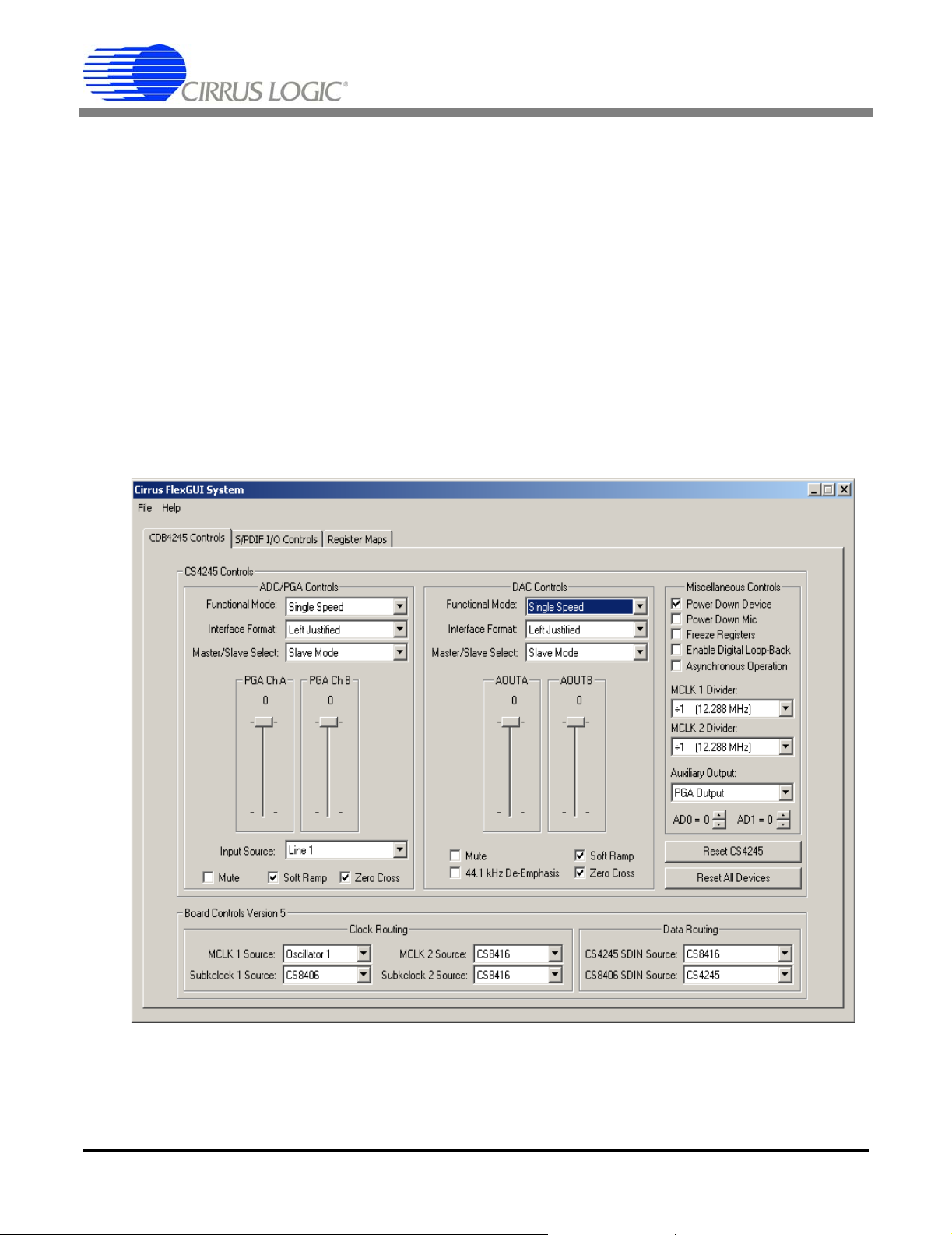
4.1 CDB4245 Controls Tab
The CDB4245 Controls tab provides a high-level intuitive interface to many of the configuration options of
the CS4245 and CDB4245. The controls within the CS4245 Controls group box (with the exception of the
AD0 and AD1 controls) control the internal registers of the CS4245. The con trols with in the Boar d Con trols
group box control the board level clock and data routing on the CDB4245.
Figure 1. CDB4245 Controls Tab
DS656DB1 7
Page 8
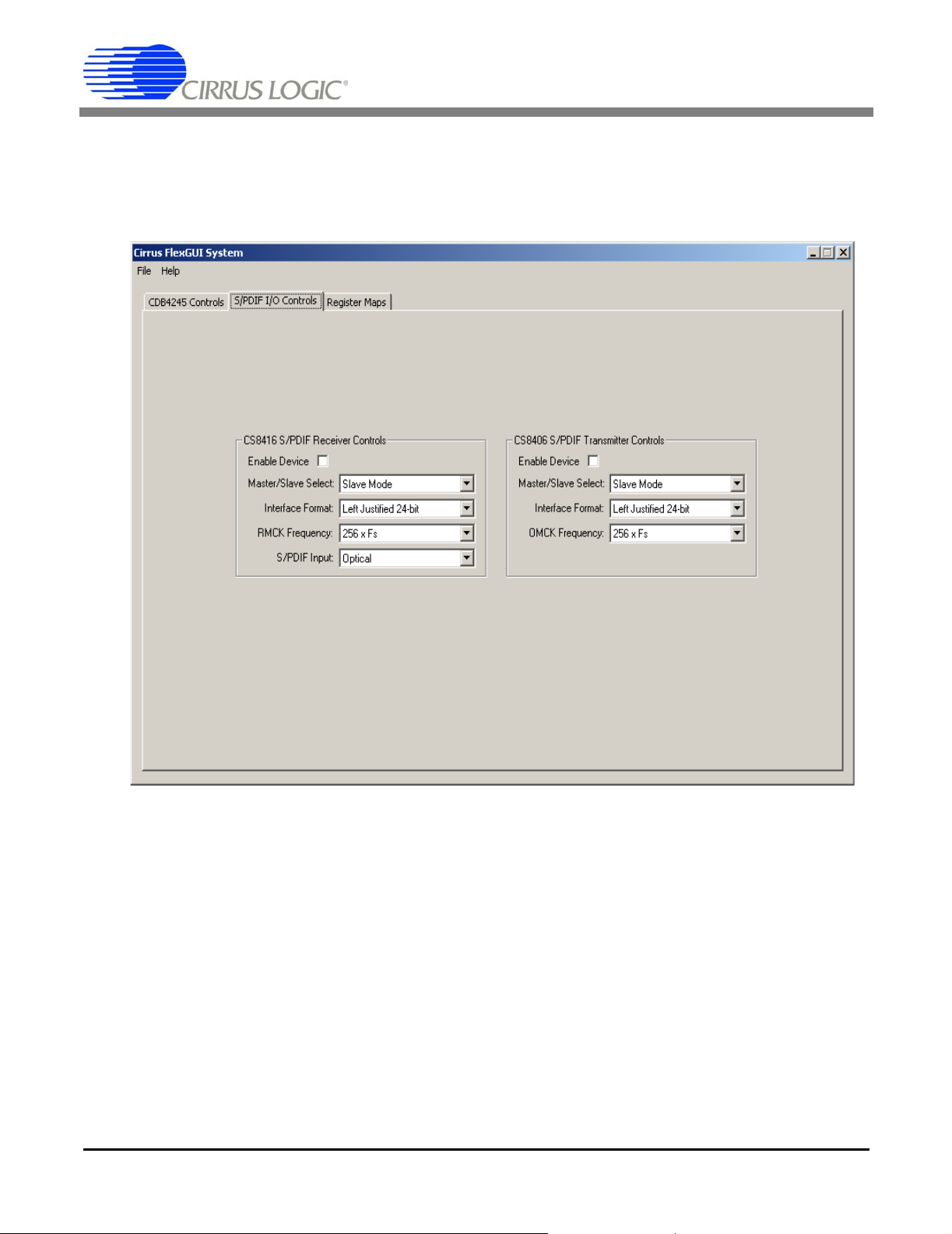
4.2 S/PDIF I/O Controls Tab
When the CDB4245 is configured to make use of the CS8416 S/PDIF receiver or CS8406 S/PDIF transmitter, these devices must be c onfigured for proper operation. The S/PDIF I/O Controls tab provides a highlevel intuitive interface to the most common configuration options of the CS8416 and CS8406.
CDB4245
Figure 2. S/PDIF I/O Controls Tab
8 DS656DB1
Page 9
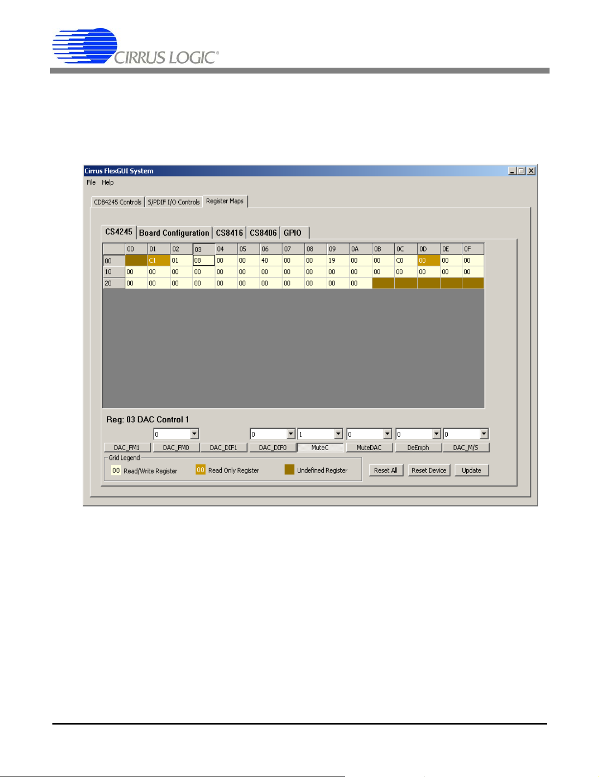
4.3 Register Maps Tab
The Register Maps tab provides low level control over the register level settings of the CS4245, CS8416,
CS8406, and FPGA. Each device is displayed on a separate tab. Register values can be modified bit-wise
or byte-wise. For bit-wise, click the appropriate push button for the desired bit. For byte-wise, the desired
hex value can be typed directly in the register address box in the register map.
CDB4245
Figure 3. Register Maps Tab
4.4 Pre-Configured Script Files
Pre-configured script files are provided with the CDB4245 to allow easy initial board bring-up. The board
configurations stored within these files are described in sections 4.4.1 - 4.4.2.
4.4.1 Oscillator Clock - ADC Ch 1 to DAC & SPDIF Out
Using the pre-configured script file named “Oscillator Clock - ADC Ch 1 to DAC & SPDIF Out.txt”, an analog
input signal applied to channel 1 of the CS4245 input multiplexer will be digitized by the ADC, transmitted
in S/PDIF format by the CS8406, and will be converted to analog by the CS4245 DAC and output through
the passive output filter and RCA jacks.
The CS4245 is in synchronous mode, with Oscillator 1 as the source of MCLK for Clock Domain 1 and 2.
The CS4245 Serial Audio Port 1 is the sub-clock master to both the CS4245 Serial Audio Port 2, and the
CS8406.
DS656DB1 9
Page 10

CDB4245
4.4.2 SPDIF Recovered Clock - SPDIF to DAC & ADC to SPDIF
Using the pre-configured script file named “SPDIF Recovered Clock - SPDIF to DAC & ADC to SPDIF.txt”,
an analog input signal applied to channel 1 of the CS4245 input multiplexer will be digitized by the ADC,
transmitted in S/PDIF format by the CS8406. A S/PDIF input signal will be converted to analog by the
CS4245 DAC and output through the passive output filter and RCA ja cks. For proper operation of this scrip t,
a valid S/PDIF signal must be applied.
The CS4245 is in synchronous mode, with the CS8416 as the source of MCLK for Clock Domain 1 and 2.
The CS8416 is also the sub-clock master to both the CS4245 Serial Audio Port 1 and 2, as well as the
CS8406.
10 DS656DB1
Page 11

CDB4245
5. FPGA REGISTER QUICK REFERENCE
This table shows the register names and their associated default values.
Addr Function 7 6 5432 1 0
Code Rev. ID
01h
MCLK Source
02h
Subclock
03h
Source
CS4245 SDIN
04h
Source
Transmitter
05h
SDIN Source
Rev7 Rev6 Rev5 Rev4 Rev3 Rev2 Rev1 Rev0
xxxxxx x x
Reserved Reserved MCLK2.1 MCLK2.0 Reserved Reserved MCLK1.1 MCLK1.0
001000 0 0
Reserved Reserved DAC1 DAC0 Reserved Reserved ADC1 ADC0
000100 0 1
Reserved Reserved Reserved Reserved Reserved Reserved SDIN1 SDIN0
000000 0 0
Reserved Reserved CS8406.1 CS8406.0 Reserved Reserved Reserved Reserved
000100 0 1
DS656DB1 11
Page 12

CDB4245
6. FPGA REGISTER DESCRIPTION
6.1 CODE REVISION ID - ADDRESS 01H
76543210
Rev7 Rev6 Rev5 Rev4 Rev3 Rev2 Rev1 Rev0
Function:
Identifies the revision of the FPGA code. This register is Read-Only.
6.2 MCLK SOURCE CONTROL - ADDRESS 02H
76543210
Reserved Reserved MCLK2.1 MCLK2.0 Reserved Reserved MCLK1.1 MCLK1.0
6.2.1 MCLK2 SOURCE (BITS 5:4)
Default = 10
Function:
These bits select the source of the CS4245 MCLK2 signal. Table 1 shows the available settings.
Table 1. MCLK2 Source
MCLK2.1 MCLK2.0 MCLK2 Source
0 0 Oscillator 2
0 1 MCLK2 position on Header 2
1 0 CS8416 RMCK
11 MCLK1
6.2.2 MCLK1 SOURCE (BITS 1:0)
Default = 00
Function:
This bit selects the source of the CS4245 MCLK1 signal. Table 2 shows the available settings.
Table 2. MCLK1 Source
MCLK1.1 MCLK1.0 MCLK1 Source
0 0 Oscillator 1
0 1 MCLK1 position on Header 1
10 Reserved
11 MCLK2
12 DS656DB1
Page 13

CDB4245
6.3 SUBCLOCK SOURCE CONTROL - ADDRESS 03H
76543210
Reserved Reserved DAC1 DAC0 Reserved Reserved ADC1 ADC0
6.3.1 DAC SUBCLOCK SOURCE (BITS 5:4)
Default = 01
Function:
These bits select the source of the CS4245 SCLK2 and LRCK2 signals. Table 3 shows the available
settings.
T able 3. DAC Subclock Source
DAC1 DAC0 DAC Subclock Source
0 0 - CS4245 is Master
- Header 2 Subclocks are Output from CS4245
0 1 - CS4245 is Slave to CS8416
- Header 2 Subclocks are Output from CS8416
1 0 - CS4245 is Slave to Header
1 1 - CS4245 is Slave to ADC subclocks
- Header 2 Subclocks are Output from ADC subclocks
- CS8416 is Slave to CS4245
- CS8416 is Master
- CS8416 is Slave to Header
- Header 2 subclocks are an Input
- CS8416 is Slave to ADC subclocks
6.3.2 ADC SUBCLOCK SOURCE (BITS 1:0)
Default = 01
Function:
This bit selects the source of the CS4245 SCLK1 andLRCK1 signals. Table 4 shows the available settings.
T able 4. ADC Subclock Source
ADC1 ADC0 ADC Subclock Source
0 0 - CS4245 is Master
- Header 1 Subclocks are Output from CS4245
0 1 - CS4245 is Slave to CS8406
- Header 1 Subclocks are Output from CS8406
1 0 - CS4245 is Slave to Header
1 1 - CS4245 is Slave to DAC subclocks
- Header 1 Subclocks are Output from DAC subclocks
- CS8406 is Slave to CS4245
- CS8406 is Master
- CS8406 is Slave to Header
- Header 1 subclocks are an Input
- CS8406 is Slave to DAC subclocks
DS656DB1 13
Page 14

CDB4245
6.4 CS4245 SDIN SOURCE CONTROL - ADDRESS 04H
76543210
Reserved Reserved Reserved Reserved Reserved Reserved SDIN1 SDIN0
6.4.1 SDIN SOURCE (BITS 1:0)
Default = 00
Function:
These bits select the source of the CS4245 SDIN1 signal. Table 5 shows the available settings.
Table 5. SDIN1 Source
SDIN1 SDIN0 SDIN Source
0 0 CS8416 SDOUT
0 1 CS4245 SDOUT
1 0 SDIN from Header
11 Reserved
6.5 TRANSMITTER SDIN SOURCE CONTROL - ADDRESS 05H
76543210
Reserved Reserved CS8406.1 CS8406.0 Reserved Reserved Reserved Reserved
6.5.1 CS8406 SDIN SOURCE (BITS 5:4)
Default = 00
Function:
These bits select the source of the CS8406 SDIN signal. Table 6 shows the available settings.
Table 6. CS8406 SDIN Source
CS8406.1 CS8406.0 CS8406 SDIN Source
0 0 CS8416 SDOUT
0 1 CS4245 SDOUT
1 0 SDIN from Header
11 Reserved
14 DS656DB1
Page 15

7. CDB CONNECTORS, JUMPERS, AND SWITCHES
Reference
CONNECTOR
+5V J1 Input
GND J2 Input
S/PDIF RX OPT1 Input
S/PDIF RX J13 Input
S/PDIF TX J15 Output
S/PDIF TX OPT2 Output
RS232 I/O J42 Input/Output
USB I/O J37 Input/Output
PCM1 I/O J10 Input/Output
PCM2 I/O J9 Input/Output
CONTROL J17 Input/Output
MICRO JTAG J36 Input/Output
FPGA-JTAG J18 Input/Output
MICRO RESET S2 Input
PROGRAM FPGA S1 Input
PINA
PINB
AINA
AINB
MICIN1
MICIN2
AOUTA
AOUTB
POUTA
POUTB
Designator INPUT/OUTPUT SIGNAL PRESENT
+5.0 V Power Supply
Ground Reference
CS8416 digital audio input via optical cable
CS8416 digital audio input via coaxial cable
CS8406 digital audio output via coaxial cable
CS8406 digital audio output via optical cable
Serial connection to PC for SPI / I2C control port signals
USB connection to PC for SPI / I2C control port signals.
Not Available.
I/O for Serial Audio Port 1 Clocks & Data
I/O for Serial Audio Port 2 Clocks & Data
I/O for external SPI / I2C control port signals.
I/O for programming the micro controller (U46).
I/O for programming the FPGA (U35).
Reset for the micro controller (U46).
Reset for the FPGA (U35).
J38
J39
J40
J41
J21
J34
J14
J16
J8
J11
Input RCA phono jacks for analog input signal to CS4245. Pas-
sive input filter.
Input RCA phono jacks for analog input signal to CS4245. Active
input buffer.
Input
Output
1/8“ TRS jacks for microphone input.
RCA phono jacks for auxiliary analog outputs. Active output
buffer.
Output
RCA phono jacks for DAC analog output. Passive output filter.
Table 7. System Connections
CDB4245
DS656DB1 15
Page 16

JUMPER PURPOSE POSITION FUNCTION SELECTED
J3 Selects the source of voltage for the VLC
supply.
J4 Selects the source of voltage for the VD
supply
J5 Selects the source of voltage for the VLS
supply.
J6 Selects the source of voltage for the VA
supply
J7 Selects the function of the CS4245
MUTEC
J12 Selects the function of the CS4245
MUTEC
J19
J20
J22 - J33 Maps the passive and active input circuits
Select the input type for channel 4 of the
CS4245 ADC input multiplexer.
to the CS4245 input multiplexer channels.
output.
output.
*Default factory settings
+1.8 V
+2.5 V
+3.3 V
+5 V*
+3.3 V
+5 V*
+1.8 V
+2.5 V
+3.3 V
+5 V*
+3.3 V
+5 V*
1*
2
1*
2
Line Input*
Mic Input
Passive Filter*
Active Filter
Voltage source is +1.8 V regulator.
Voltage source is +2.5 V regulator.
Voltage source is +3.3 V regulator.
Voltage source is +5 V regulator.
Voltage source is +3.3 V regulator.
Voltage source is +5 V regulator.
Voltage source is +1.8 V regulator.
Voltage source is +2.5 V regulator.
Voltage source is +3.3 V regulator.
Voltage source is +5 V regulator.
Voltage source is +3.3 V regulator.
Voltage source is +5 V regulator.
Activate LED for channel A.
Activate analog mute circuit for channel A.
Activate LED for channel B.
Activate analog mute circuit for channel B.
Select RCA input multiplexer as source.
Select TRS inputs as source.
Passive filter mapped to input MUX channel.
Active filter mapped to input MUX channel.
CDB4245
Table 8. System Jumper Settings
16 DS656DB1
Page 17

8. CDB BLOCK DIAGRAM
CDB4245
Passive Output Filter
Active Output Filter
Test Points
CS4245
Canned
Oscillator
Header
Control Port Interface
FPGA
Sub-clocks and Data
Figure 4. Block Diagram
X
U
M
Master Clock Master Clock
Passive Input Filter
DS656DB1 17
Active Input Filter
Microphone Input
Canned
Oscillator
Header
CS8416 CS8406
CS8416 CS8406
Page 18

9. CDB SCHEMATICS
CDB4245
Figure 5. CS4245
18 DS656DB1
Page 19

CDB4245
Figure 6. Analog Inputs
DS656DB1 19
Page 20

CDB4245
Figure 7. Analog Outputs
20 DS656DB1
Page 21

CDB4245
Figure 8. S/PDIF I/O
DS656DB1 21
Page 22

CDB4245
Figure 9. Control Port
22 DS656DB1
Page 23

CDB4245
Figure 10. FPGA
DS656DB1 23
Page 24

CDB4245
Figure 11. Discrete Clock Routing and Level Shifting
24 DS656DB1
Page 25

CDB4245
Figure 12. Power
DS656DB1 25
Page 26

10.CDB LAYOUT
CDB4245
Figure 13. Silk Screen
26 DS656DB1
Page 27

CDB4245
Figure 14. Topside Layer
DS656DB1 27
Page 28

CDB4245
Figure 15. Bottom side Layer
28 DS656DB1
Page 29

11.REVISION HISTORY
Revision Date Changes
DB1 February 2005 Initial Release
Table 9. Revision History
CDB4245
Contacting Cirrus Logic Support
For all product questions and inquiries contact a Cirrus Logic Sales Representative.
To find one nearest you go to www.cirrus.com
IMPORTANT NOTICE
Cirrus Logic, Inc. and its subsidiaries ("Cirrus") believe that the information contained in this document is accurate and reliable. However, the infor-
mation is subject to change without notice and is provided "AS IS" without warranty of any kind (express or implied). Customers are advised to obtain
the latest version of relevant information t o verify, before placing orders, that inf ormation being relied on is curre nt and complete. All products are
sold subject to the terms and conditions of sale supplied at the time of order acknowledgment, including those pertaining to warranty, indemnification,
and limitation of liability. No responsibility is assumed by Cirrus for the use of this information, including use of this information as the basis for manufacture or sale of any item s, or f or i nf ring eme nt of patents or o t her r ig hts of t hird partie s. Th is do cum ent i s th e p roper t y o f Cirrus and by furnishing
this information, Cirrus g rants no license, express or implied under an y patents, mask work rights, cop yrights, trademarks, tr ade secrets or other
intellectual property rights. Cirr us own s th e copy ri gh ts associ at ed w ith t he inf o rmati o n con tained he re in an d gi ves co nse nt for c opi e s to be mad e of
the information only for use within your organization with respect to Cirrus integrated circuits or other products of Cirrus. This consent does not extend
to other copying such as copyin g for general distribution, advertising or promotional purposes, or for creating any work for resale.
CERT AIN APPLICA TIONS USING SEMICONDUCTOR PRODUCTS MA Y INVOLVE POTENTIAL RISKS OF DEATH, PERSONAL INJURY, OR SEVERE PROPERTY OR ENVIRONMENTAL DAMAGE ("CRITICAL APPLICATIONS"). CIRRUS PRODUCTS ARE NOT DESIGNED, AUTHORIZED
OR WARRANTED FOR USE IN AIRCRAFT SYSTEMS, MILITARY APPLICATIONS, PRODUCTS SURGICALLY IMPLANTED INTO THE BODY,
AUTOMOTIVE SAFETY OR SECURITY DEVICES, LIFE SUPPORT PRODUCTS OR OTHER CRITICAL APPLICATIONS. INCLUSION OF CIRRUS PRODUCTS IN SUCH APPLICATIONS IS UNDERSTOOD TO BE FULLY AT THE CUSTOMER'S RISK AND CIRRUS DISCLAIMS AND
MAKES NO WARRANTY, EXPRESS, STATUTORY OR IMPLIED, INCLUDING THE IMPLIED WARRANTIES OF MERCHANTABILITY AND FITNESS FOR PARTICULAR PURPOSE, WITH REGARD TO ANY CIRRUS PRODUCT THAT IS USED IN SUCH A MANNER. IF THE CUSTOMER
OR CUSTOMER'S CUSTOMER USES OR PERMITS THE USE OF CIRRUS PRODUCTS IN CRIT ICAL APPL ICATIONS, CUSTOMER AGREES,
BY SUCH USE, TO FULLY INDEMNIFY CIRRUS, ITS OFFICERS, DIRECTORS, EMPLOYEES, DISTRIBUTORS AND OTHER AGENTS FROM
ANY AND ALL LIABILITY , INCLUDING A TT ORNEYS' FEES AND COSTS, THA T MAY RESULT FROM OR ARISE IN CONNECTION WITH THESE
USES.
Cirrus Logic, Cirrus, the Cirr us Logic log o designs, an d Popguard are tradema rks of Cirru s Logic, Inc. All other br and and prod uct names in this doc ument may be trademarks or service mar ks of their respective owners.
Windows is a registered trademark of Microsoft Corporation.
DS656DB1 29
 Loading...