

Page 1
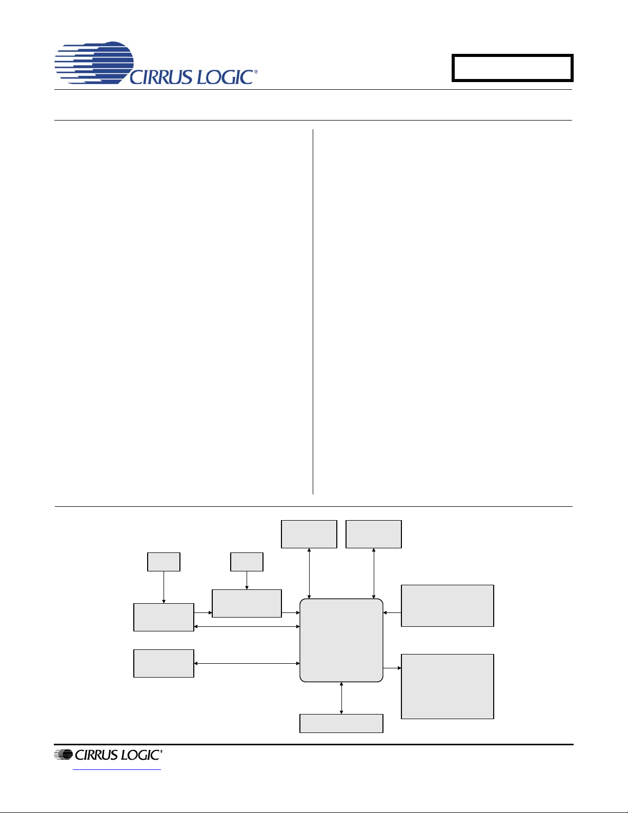
CS4244 Evaluation Board
CS4244
S/PDIF Input
(CS8416)
S/PDIF Output
(CS8406)
Clock Synthesis
(CS2000)
Osc. Crystal
DSP Header
Control
Header
USB Control
Port
Analog Inputs
- Active Single Ended to
Differential
- Passive Differential
Analog Outputs
- Passive Single Ended
& Differential
- Active Single Ended &
Differential
- Active Differential to
Single Ended
CDB4244
Features
Multiple Analog Input Filter Options
– Active Single Ended to Differential
– Passive Differential
Multiple Analog Output Filter Options
– Passive Single Ended & Differential
– Active Single Ended & Differential
– Active Differential to Single Ended
Versatile S/PDIF Interface
– CS8416 Digital Audio Receiver
– CS8406 Digital Audio Transmitter
– CS2000 Clock Synthesizer
External Connection Headers
– Control Port Accessibility
– DSP Serial Audio I/O Accessibility
Windows
– Allows Easy Configuration of the CDB4244
– Predefined & User-Configurable Scripts
®
Compatible FlexGUI S/W Control
Description
The CDB4244 evaluation board is an excellent platform
designed to facilitate evaluation of the CS4244 multichannel CODEC. Use of the board requires an analog/digital signal source, an audio analyzer, and power
supplies. A Windows
needed in order to configure the board.
System timing for the I²S and Left-Justified serial interface formats can be accomplished using S/PDIF I/O or
crystal-based timing hardware on the CDB42 44. An e xternal DSP interface header supports I²S, Left-Justified,
and TDM serial interface formats.
1/8” audio jacks, three-pin headers, and RCA phono
jacks are provided for the CS4244 analog I/O connections. Digital I/O connections are accomplished through
RCA phono jacks or optical connectors leading to the
S/PDIF receiver and transmitter.
The Windows-based software available online makes
configuring the CDB4244 easy. The software communicates through the PC’s USB port to control the
CS4244, the S/PDIF receiver and transmitter, and the
clock synthesizer. These devices can also be controlled through an external control header for easy insystem evaluation.
ORDERING INFORMATION
CDB4244 Evaluation Board
PC-compatible computer is also
http://www.cirrus.com
Copyright Cirrus Logic, Inc. 2011
(All Rights Reserved)
MAR '11
DS900DB2
Page 2

TABLE OF CONTENTS
1 SYSTEM OVERVIEW ..............................................................................................................................4
1.1 Power ...............................................................................................................................................4
1.2 Grounding and Power Supply Decoupling ....................................................................................... 4
1.3 CS4244 Multi-Channel CODEC ....................................................................................................... 4
1.4 CS8406 Digital Audio Transmitter ....................................................................................................4
1.5 CS8416 Digital Audio Receiver ........................................................................................................5
1.6 CS2000 Fractional-N Clock Synthesizer & Clock Multiplier ............................................................. 5
1.7 Oscillator .......................................................................................................................................... 5
1.8 External Connection Headers ..........................................................................................................5
1.9 Analog Inputs ................................................................................................................................... 6
1.10 Analog Outputs ......................................... ... ..................................................................................6
2 SOFTWARE MODE CONTROL ............... ... ... .... ... ... ... .... ........................................................................ 7
2.1 Board Control Tab ............................................................................................................................8
2.2 CODEC Control Tab ........................................................................................................................9
2.3 Volume Control Tab .......................................................................................................................10
2.4 Register Maps Tab ......................................................................................................................... 11
2.5 Predefined Sample Scripts ............................................................................................................ 12
3 MASTER CLOCK CONFIGURATION ...................................................................................................13
3.1 CS8416 Recovered Master Clock ..................................................................................................13
3.2 CS2000-Generated Master Clock .................................................................................................. 14
3.3 CS2000 Timing Reference .............................................................................................................14
3.4 Miscellaneous Options ................................................................................................................... 14
4 ANALOG INPUT FILTERS .................................................................................................................... 15
4.1 Active Single-Ended-to-Differential Input Filter .............................................................................. 15
4.2 Passive Differential Input Filter ...................................................................................................... 15
4.3 Analog Input Filter Configuration ................................................................................................... 16
5 ANALOG OUTPUT FILTERS ................................................................................................................ 17
5.1 Analog Output Filter Considerations ..............................................................................................17
5.2 Analog Output Filter Configuration .................................................................................................19
6 SYSTEM CONNECTIONS AND JUMPER PIN BLOCKS ..................................................................... 20
6.1 System Connections ...................................................................................................................... 20
6.2 Jumper Pin Blocks .........................................................................................................................21
6.3 Test Points ..................................................................................................................................... 21
7 CDB4244 BLOCK DIAGRAM ...............................................................................................................22
8 CDB4244 SCHEMATIC ......................................................................................................................... 23
9 CDB4244 LAYOUT ................................................................................................................................ 31
10 REVISION HISTORY ........................ ... ... ... ... .................................................................... ...................36
CDB4244
LIST OF FIGURES
Figure 1.Board Control Tab ............................. ... .... ... ... ... .... ... ... ... .... ... ... ... ... .... ... ........................................ 8
Figure 2.CODEC Control Tab ................................... ... ... .... ... ... ... .... ... ... ... ... ............................................... 9
Figure 3.Volume Control Tab ................................. ... ... ... .......................................................................... 10
Figure 4.Register Maps Tab ............................ ... .... ... ... ... .... ... ... ... .... ... ... ... ... .... ......................................... 11
Figure 5.Master Clock Path ....................... ... ... ... .... ... ... ... ..........................................................................13
Figure 6.Active Single-Ended-to-Differential Input Filter Block Diagram ................ ... .... ... ... ... ...................15
Figure 7.Passive Differential Input Filter Block Diagram ........ .......................................... ......................... 15
Figure 8.Analog Output Filter Block Diagram ............................................................................................17
Figure 9.CDB4244 Block Diagram .................................. .... ... ... ... .... ... ... ... ... .... ... ... ... ................................ 22
Figure 10.CS4244 (Schematic Sheet 1) ................ ... ... ... .... ... ................................................................... 23
Figure 11.S/PDIF I/O (Schematic Sheet 2) ...............................................................................................24
Figure 12.USB I/O (Schematic Sheet 3) ...................................................................................................25
Figure 13.Analog Input Channels 1 & 2 (Schematic Sheet 4) ................................................................... 26
2 DS900DB2
Page 3

Figure 14.Analog Input Channels 3 & 4 (Schematic Sheet 5) ................................................................... 27
Figure 15.Analog Output Channels 1 & 2 (Schematic Sheet 6) ................................................................28
Figure 16.Analog Output Channels 3 & 4 (Schematic Sheet 7) ................................................................29
Figure 17.Power (Schematic Sheet 8) ......................................................................................................30
Figure 18.Silk Screen ................................................................................................................................31
Figure 19.Top Side (Layer 1) ....................................................................................................................32
Figure 20.Ground Plane (Layer 2) ............... ... ... .... ... ... .............................................................................33
Figure 21.Power Plane (Layer 3) ..............................................................................................................34
Figure 22.Bottom Side (Layer 4) ............................................................................................................... 35
LIST OF TABLES
Table 1. Analog Input Filter Components ..................................................................................................16
Table 2. Analog Output Filter Components .. ... ... ....................................................................... .... ... .........19
Table 3. System Connections ...................................................................................................................20
Table 4. Jumper Pin Blocks ...... ... ... ... .... ... ... ... .................................................................... ......................21
CDB4244
DS900DB2 3
Page 4

1 SYSTEM OVERVIEW
CDB4244
The CDB4244 platform provides analog and digital interfac es to the CS4244 and allows for external DSP and I²C
control. Board configuration can be done using the Windows PC-compatible graphical user interface (GUI) to read
and write device registers. Multiple analog input and output filter configurations are supported, as well are several
different options for generating a system master clock.
The CDB4244 schematic set has been partitioned into eight pages and is shown in Section 8 starting on page 23.
Additionally, Section 6 on page 20 provides a description of all external connectors, including the default factory settings for all jumpers.
TM
1.1 Power
Power is supplied to the board through an external regulated +5-V supply or a PC USB port. The CS4244
analog supply (referred to as VA) may be taken from the selected +5-V supply or an onboard +3.3-V regulator. Table 4 on page 21 explains how to configure each option. A dual-rail ±12-V regulated supply is required to power the active filter network used for each analog input channel. A special resistor option allows
the optional active analog output filter configurations to use either a single-rail or dual-rail power supply.
Shunt jumpers and 1%, 1-Ω parallel resistors provide a convenient way to measure both the VA and VL
supply currents to the CS4244. The current is easily calculated by measuring the vol tage drop across each
resistor with its associated shunt removed. The shunts connected in parallel with these resistors must be in
place during normal operation.
WARNING: Please refer to the CS4244 data sheet for allowable voltage levels.
1.2 Grounding and Power Supply Decoupling
The CS4244 requires careful attention to power supply and grounding arrangements to optimize performance. The CDB4244 demonstrates these optimal arrangements. Figur e 18 on page 31 shows the component placement; Figure 19 on page 32 shows the top-side layout and Figure 22 on page 35 shows the
bottom-side layout. Power supply decoupling capacitors are located as close as possible to the CS4244.
Extensive use of ground plane fill helps reduce radiated noise.
1.3 CS4244 Multi-Channel CODEC
A complete description of the CS4244 (Figure 10 on page 23) can b e found in the CS42 44 da ta shee t. The
CS4244 is configured using the Cirrus Logic FlexGUI software. The device configuration registers are accessible via the “Register Maps” tab of the software. This tab provides low-level control of each bit in the
device’s control port. The “CODEC Control” and “Volume Control” tabs p rovide high- level co ntrol of the d evice for faster configuration. See Section 2 on page 7 for details.
1.4 CS8406 Digital Audio Transmitter
The CS8406 S/PDIF transmitter (Figure 11 on page 2 4) converts the digital audio generated by th e CS4244
(I²S or Left-Justified serial interface formats) to the standard S/PDIF data stream and routes these signals
to the optical and RCA connectors on the CDB4244. With a supplied master clock, the CS8406 can master
the serial audio interface timing for the CDB4244.
The CS8406 can be controlled using the Cirrus Logic FlexGUI software under the “Board Control” tab. See
Section 2.1 on page 8 for details. A complete description of the CS8406 and a discussion of the digi tal audio
interface can be found in the CS8406 data sheet.
4 DS900DB2
Page 5

1.5 CS8416 Digital Audio Receiver
The CS8416 S/PDIF receiver (Figure 11 on page 24) converts the incoming S/PDIF data stream from the
optical or RCA connectors into digital audio (I²S or Left-Justified serial interface formats) and passes it to
the CS4244. Using the master clock recovered from the incoming S/PDIF stream or the clock provided by
the socketed onboard oscillator, the CS8416 can master the serial audio interface timing for the CDB4244.
The CS8416 can be controlled using the Cirrus Logic Fl exGUI software under the “Board Control” tab. See
Section 2.1 on page 8 for details. A complete description of the CS8416 and a discussion of the digital audio
interface can be found in the CS8416 data sheet.
1.6 CS2000 Fractional-N Clock Synthesizer & Clock Multiplier
The CS2000 clock synthesize r (Figure 11 on page 24) provides a low-jitter master clock source for the
CS4244 and CS8406, and is capable of generating th e necessary master clock frequen cies to provide multiple sample rates without having to make hardware changes to the board. The Cirrus Logic FlexGUI software can be used to easily realize many of the clocking options available for the CDB4244.
Refer to Section 3 on page 13 for a detailed expla nation of how the CS2000 can be used wi th the CDB4244.
A complete description of the CS2000 can be found in the CS2000 data sheet.
1.7 Oscillator
The socketed onboard oscillator (Figure 11 on page 24) can serve as the master clock for the CDB4244
when the CS8416 can no longer recover a master clock from the incoming S/PDIF stream. Refer to Section
3.1 on page 13 for more information. The oscillator is mounted in pin sockets, allowing easy removal or re-
placement. The CDB4244 can accommodate +5-V half-can oscillators.
CDB4244
1.8 External Connection Headers
The CDB4244 has been de signed to allow connections to and from an external system through a DSP
header (J2 in Figure 10 on page 23) and a control port header (J1 in Figure 10 on p age 23). The DSP header
provides access to the serial audio signals required to interface with an external system. The control port
header provides bidirectional access to the I²C control port signals. Two unp opulated pull-up resistors (R165
and R166) are also available in the event that the external host does not have pull-up resistors on its I²C
lines.
These headers are accessed by removing the jumpers from the “Jumper for Bd Control” positio n labeled on
the board. The user may then connect a ribbon cable connector to the “Ext Control Connection” pins for
external control of the CDB4244. A single row of “GND” pins are provided to maintain signal ground integrity.
If the headers are not in use, the jumpers must be in place for each row of J1 and J2 in the “Jumper for Bd
Control” position. In this configuration, the CDB4244 assumes full control of the CS4244, with access
through the PC USB connection.
Note that the CS4244 INT
have a pull-up resistor to pull the interrupt signal high once it is deasserted by the CS4244. Instead, the interrupt signal is pulled high by a pull-up resisto r internal to the onboard microcontroller. If the CDB4244 is
controlled externally (through the use of J1), the external system must be able to pull the interrupt signal
high if the CS4244 INT
configured as active high or active low, avoiding the need for a pull-up resistor in this case. Refer to the
CS4244 data sheet for more information.
To pass digital audio data from the ADCs of the CS4244 directly to the DACs in order to evaluate analogin-to-analog-out performance, remove the jumpers from the SDOUT1, SDIN1, SDOUT2, and SDIN2 rows
of the DSP header (J2). Then jumper SDOUT1 to SDIN1, an d SDOUT 2 to SDIN2 using the mid dle colum n
of the DSP header.
pin defaults to an active-low, open-drain interrupt output. Th e CDB4244 does not
pin remains in its default open-drain configuration. Alternatively, the INT pin may be
DS900DB2 5
Page 6

1.9 Analog Inputs
The CDB4244 can accept single-ended analog input signals through the RCA phono jacks on each channel.
An active single-ended-to-different ial input filter network converts the single-ended input into a differential
signal before the signal is passed to the respective differential analog inputs of the CS4244.
Space for a passive differential filter option allows differential analog input signals to be connected directly
to the CDB4244. Stereo 1/8” audio jacks are provided to support this option; however, the components used
to populate this filter option must be obt ained separa tely. With either filter option, analog input signals are
AC-coupled to the CS4244.
Refer to Section 4 starting on page 15 for details on the implementation of either input filter.
1.10 Analog Outputs
The CDB4244 provides differential analog outputs through the stereo 1/8 ” audio jacks on each output channel. While a passive filter network is populated on each output channel by default, each channel has space
for an optional active differential filter network.
Both the active and passive differential filter options can be converted to provide single-ended outputs by
removing certain components from the board. A fifth filter option provides space for an active differential-tosingle-ended filter, which can convert the differentia l analog outputs of the CS4 244 into a single- ended signal. RCA phono jacks are provided to support these options. The components used to populate any of the
three active output filter options available for each channel must be obtained separately.
CDB4244
Refer to Section 5 starting on page 17 for details on the implementation of each output filter.
6 DS900DB2
Page 7
CDB4244
2 SOFTWARE MODE CONTROL
The CDB4244 can be used with the Microsoft Windows®–based FlexGUI graphical user interface, allowing software
control of the CS4244, CS8416, CS8406, and CS2000 registers. The latest control software can be downloaded
from www.cirrus.com/msasoftware. Step-by-step instructions for setting up the FlexGUI with the CDB4244 configured under the factory default settings are provided as follows:
1. Download and install the FlexGUI software as instructed on the Cirrus Logic website.
2. Connect a triple-output power supply to the binding posts marked “+5 V EXT, GND, -12 V, and +12 V.”
3. Connect the CDB4244 to the host PC using a USB cable.
4. Launch the Cirrus Logic FlexGUI. Once the GUI is launched successfully, all CS4244 registers are set to
their default reset state, with the remaining devices preconfigured as necessary.
5. Refresh the GUI by clicking on the “Update” button. The state of all registers is now visible.
For standard setup:
1. Set up the board’s clocking and data options in the “Board Control” tab as desired.
2. Set up the CS4244 in the “CODEC Control” and “Volume Control” tabs as desired.
3. Begin evaluating the CS4244.
For quick setup, the CDB4244 may, alternatively, be configured by loading a predefined sample script file:
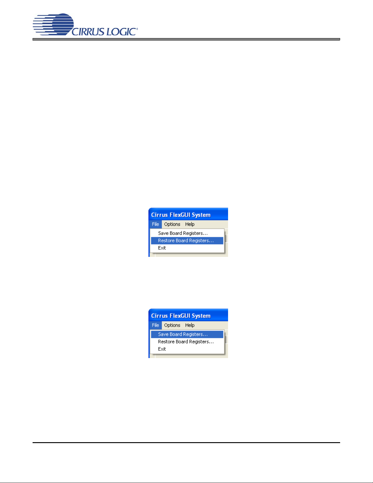
1. On the File menu, click "Restore Board Registers..."
2. Br ows e to the “Bo ard s\CDB4244\Scripts” directory.
3. Choose any one of the provided scripts to begin evaluation.
To create custom script files:
1. O n the File menu , click "Sa ve Boar d Reg ist er s.. ."
2. Enter any name that sufficiently describes the current setup.
3. Choose the desired location, and save the script.
4. To load this script at a later time, follow the instructions above for loading a predefined sample s crip t.
DS900DB2 7
Page 8
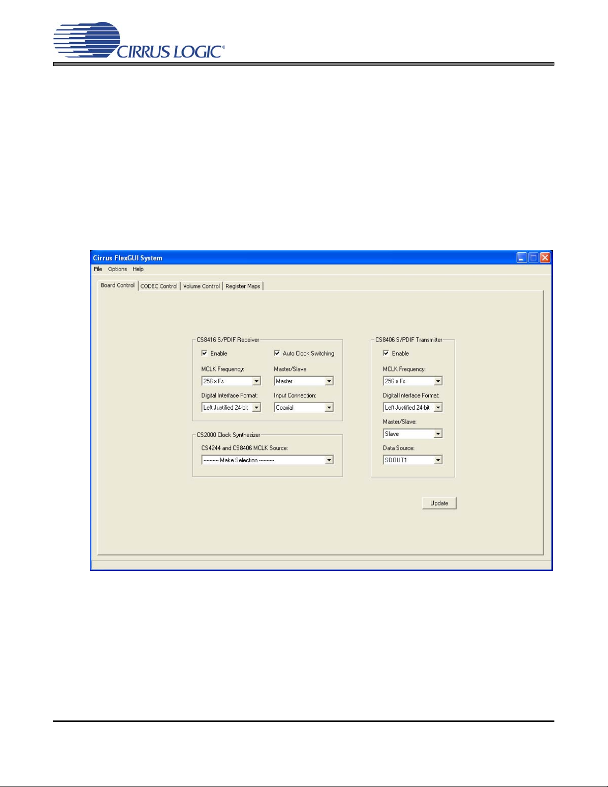
2.1 Board Control Tab
The “Board Control” tab provides high-level contr ol of the clocking and data options within the CDB4244. A
description of each control group is outlined below.
CS8416 S/PDIF Receiver—Configures the serial interface format of the S/PDIF receiver and indicate s how
the receiver is connected to the external transmitter (coaxial or optical).
CS8406 S/PDIF Transmitter—Configures the serial interface format of the S/PDIF transmitter and selects
which data channel is passed to the outgoing S/PDIF stream: SDOUT1 (ADC1 and ADC2 ) or SDOUT2
(ADC3 and ADC4).
CS2000 Clock Synthesizer—Selects the master clock that is presented to the CS4244 and CS8406. Refer
to Section 3 on page 13 for more information.
Update—Reads the registers of each device within the CDB4244 an d reflects the current values in the GUI.
CDB4244
Figure 1. Board Control Tab
Note: Refer to the CS4244 data sheet for information on how to configure the device’s clocking options
in order to satisfy the device’s recommended power up and power down sequence.
8 DS900DB2
Page 9
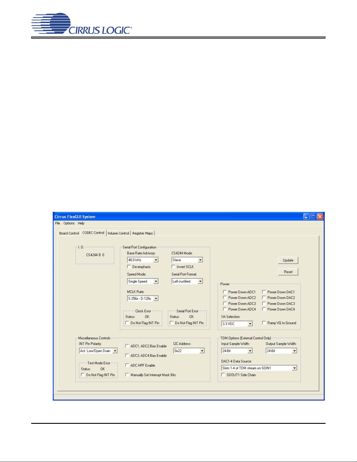
2.2 CODEC Control Tab
The “CODEC Control” tab provides high-level control of many CS4244 register settings. Status text detailing
the CODEC’s specific configuration is shown as part of certain controls. The text shown depends on the
setting of the associated control. Note that the Update button (described below) must be pressed to show
the current status of the CS4244 registers represented in this tab. A description of each control group is
outlined below. See the CS4244 data sheet for complete register descriptions.
Serial Port Configuration—Configures the CS4244’s serial port and provides controls for r ela ted inter rupts.
Note that changes to these settings durin g nor mal oper ation may violate the de vice’s recommende d power
up or power down sequence; refer to the CS4244 data sheet for more information.
Power—Provides a means to power up or power down each ADC and DAC of the CS4244. Note that it is
the user’s responsibility to ensure that the “VA Selection” control correctly reflects the VA supply level.
Miscellaneous Controls—Configures interrupt behavior and various ADC options, as well as selects the
CS4244’s I²C address.
TDM Options—Configures the CS4244’s serial port when operating in the TDM interface format. Note that
the CS4244 cannot operate in TDM mode using the CDB4244 alone; instead the CS4244 must be controlled externally to exercise the device’s TDM capabilities. Refer to Section 1.8 on page 5 for more information on how to release the CS4244 from the board’s command and control it with an external device.
Update—Reads all registers in the CS4244 and reflects the current values in the GUI.
CDB4244
Reset—Resets the CS4244.
Figure 2. CODEC Control Tab
DS900DB2 9
Page 10
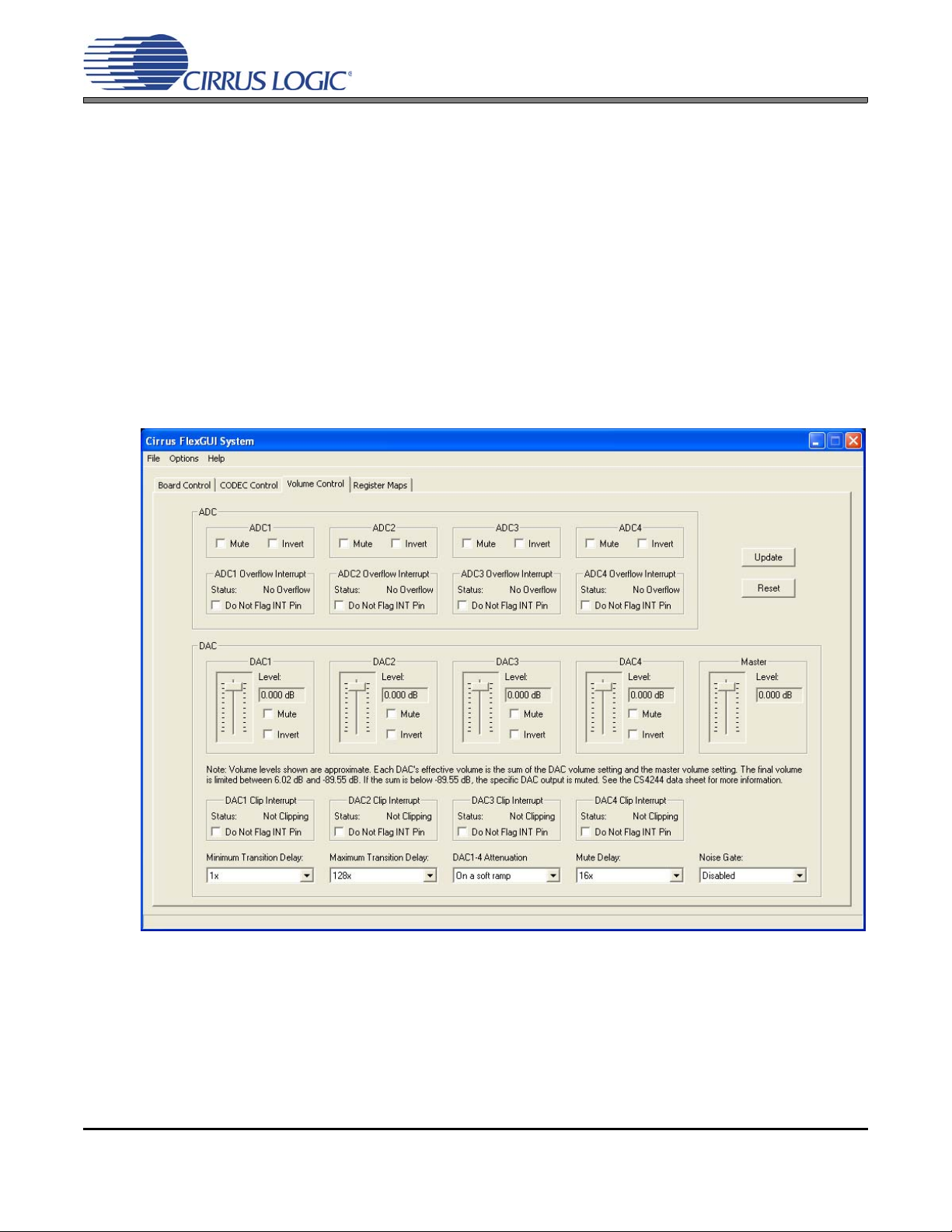
2.3 Volume Control Tab
The “Volume Control” tab provides high-le vel cont rol of all volu me-re late d settings for each ADC and DAC
of the CS4244. Status text detailing the CODEC’s specific configuration is shown as part of certain controls.
The text shown depends on the setting of the associated control. Note that the Update button (described
below) must be pressed to show the current status of the CS4244 registers represented in this tab. A description of each control group is outlined below. See the CS4244 data sheet for complete registe r descriptions.
ADC—Provides controls to mute or invert the output of each ADC and to control ADC overflow interrupts.
DAC—Provides volume, muting, and inversion controls for each DAC, as well as a master volume control.
Fine volume control can be performed by clicking on the associated volume slider and using the arrow keys.
This group also controls DAC volume changes, as well as DAC clipping interrupts.
Update—Reads all registers in the CS4244 and reflects the current values in the GUI.
Reset—Resets the CS4244.
CDB4244
Figure 3. Volume Control Tab
10 DS900DB2
Page 11
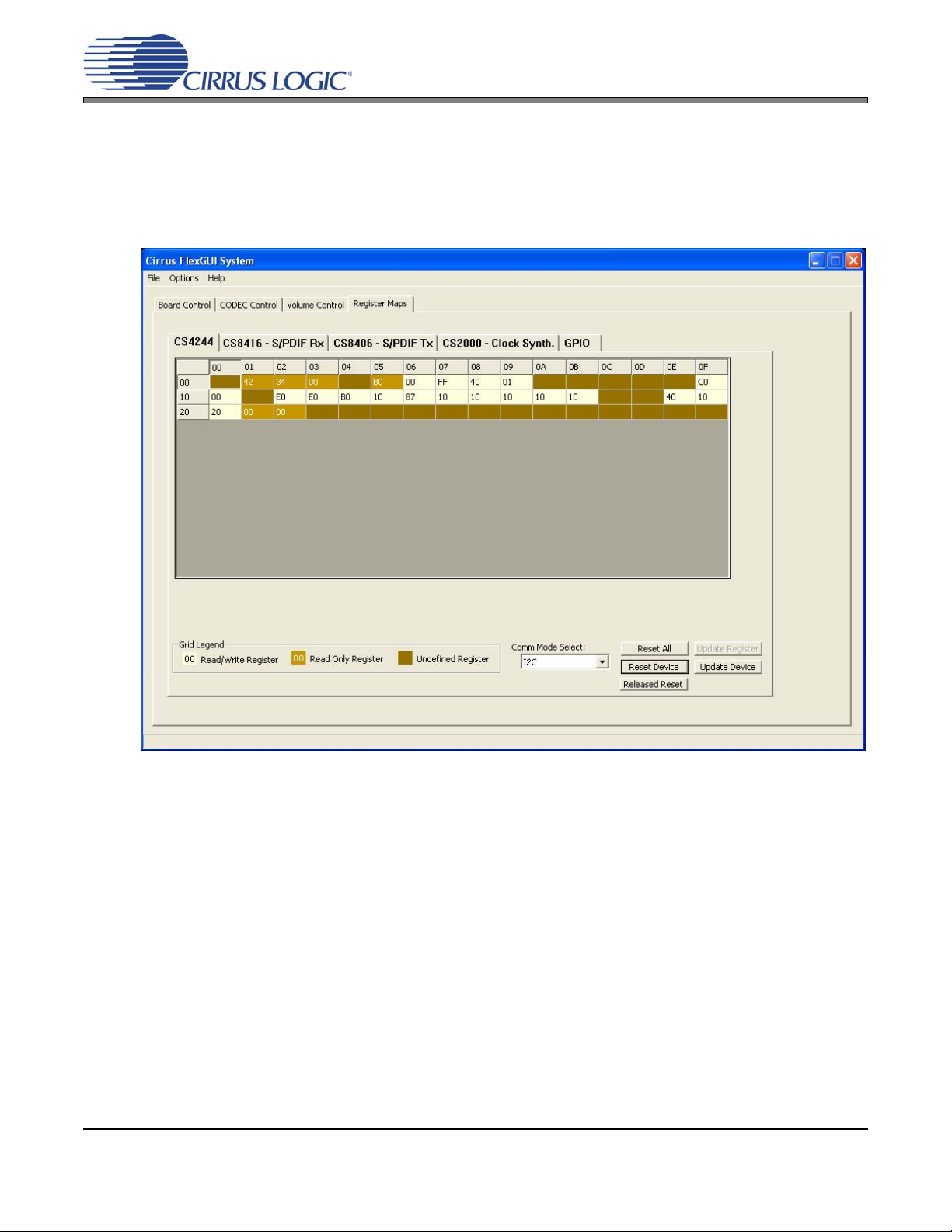
2.4 Register Maps Tab
The “Register Maps” tab provides low-level control over the register-level se ttings of the CS4244, CS84 16,
CS8406, CS2000, and microcontroller GPIO. Each device is displayed on a separate tab. Register values
can be modified bitwise or bytewise. For bitwise control, click the appropriate push button for the desired
bit. For bytewise control, the desired hexadecimal value can be type d dir ectly into the reg iste r addr ess box
within the register map.
CDB4244
Figure 4. Register Maps Tab
Certain device tabs provide a means to reset the selected device throug h the use of the “Reset Device” button. The “Released Reset/Hold In Reset” butto n provid es manu al control of the selected device’s r eset pin,
if applicable. The “Reset All” button resets the CDB4244.
The “Update Device” button reads all registers of the selected device and updates the register map accordingly. Highlighting a specific register and clicking the “Update Register” button reads only the selected register and refreshes its display in the register map.
DS900DB2 11
Page 12

2.5 Predefined Sample Scripts
The CDB4244 FlexGUI software c ome s furnished with four scripts that can quickly configure the board for
use with an external S/PDIF transmitter and receiver. These scripts configure the CS4244, CS8416, and
CS8406 to operate using the 24-bit Left-Justified serial interface format, with a master clock rate of 256
times the sample rate. The sample rate is set within the external S/PDIF source. System timing is mastered
by the CS8416 at multiples of the sample rate set by the S/PDIF source.
The system master clock recovered by the CS8416 is passed through the CS2000 before being presented
to the CS4244 and the CS8406. Serial audio data from the incoming S/PDIF stream is routed from the
CS8416 to the SDIN1 and SDIN2 pins of the CS4244, while data on the SDOUT1 pin of the CS4244 is routed to the CS8406 to be sent along the outgoing S/PDIF stream. The CS4244 is configured to operate in
single-speed mode; see the CS4244 data sheet for the ran ge of allowable in coming sample r ates. The four
scripts are defined as follows:
QuickSetup_Coax_VA_3R3V_AIN12: Configures the CDB4244 as described above when an exter-
QuickSetup_Coax_VA_5V_AIN12: Configures the CDB4244 as described above when an exter-
CDB4244
nal S/PDIF transmitter is connected to the “S/PDIF IN” input of
the board using a coaxial cable, and a 3.3-V supply is used to
power VA.
nal S/PDIF transmitter is connected to the “S/PDIF IN” input of
the board using a coaxial cable, and a 5-V supply is used to
power VA.
QuickSetup_Optical_VA_3R3V_AIN12: Configures the CDB4244 as described above when an exter-
nal S/PDIF transmitter is connected to the “S/PDIF IN” input of
the board using an optical cable, and a 3.3-V supply is used to
power VA.
QuickSetup_Optical_VA_5V_AIN12: Configures the CDB4244 as described above when an exter-
nal S/PDIF transmitter is connected to the “S/PDIF IN” input of
the board using an optical cable, and a 5-V supply is used to
power VA.
See Section 6 on page 20 regarding VA supply selection.
12 DS900DB2
Page 13

CDB4244
CS8416 CS2000
Osc.
CS4244
S/PDIF IN
CS8406
RMCK MCLK
OMCK
OMCK
S/PDIF OUT
AUX_OUTCLK_IN
Crystal
3 MASTER CLOCK CONFIGURATION
The CDB4244 offers many options for generating a system master clock. The master clock can be recovered from
the incoming S/PDIF stream by the S/PDIF receiver or sourced from the socketed onboard oscillator in the event
that the S/PDIF receiver’s internal PLL becomes unlocked. This clock can be passed directly to the CS4244 and
CS8406, or it can be passed through the CS2000 first to reduce jitte r. Alternatively, the CS2000 can be used to generate a system master clock based on the onboard 16- MHz crystal. This option can be used to exercise 18 common
master clock and sampling frequency combinations supported by the CS4244. Each of these options can be quickly
realized using the FlexGUI software, with no change in hardware required. Figure 5 highlights how these compo-
nents work together.
Figure 5. Master Clock Path
Note that the CS8416 S/PDIF receiver and the CS2000 are the only devices on the CDB4244 that can provide a
system master clock. However, the S/PDIF receiver, S/PDIF transmitter, and CODEC are all capable of mastering
system timing under the I²S and Left-Justified serial interface formats. Each device can be configured as master or
slave using the FlexGUI software. It is the user’s responsibility to ensure that only one device serves as master, with
the remaining devices configured as slaves.
3.1 CS8416 Recovered Master Clock
By default, the master clock presented to the CS4244 and CS8406 is generate d by the delta-sigma fractional-N frequency synthesizer of the CS2000. This low-jitter clock source is matched in fr equency to the master
clock recovered by the CS8416. The FlexGUI software enables this optio n at startup. This configuration can
be restored by selecting the “CS8416 Recovered MCLK (Clean)” option under the “CS4244 and CS8406
MCLK Source” menu in the “Board Control” tab (see Section 2.1 on page 8 for more information).
In the event that the CS8416’s internal PLL becomes unlocked, the CS8416 automa tically sources the master clock from the socketed oscillator. This assumes the “Auto Clock Switching” box in the “CS8416 S/PDIF
Receiver” group is checked. In this case, different master clock frequencies (and hence different sample
rates) can be realized by replacing the socketed oscillator with oscillators of different frequencies.
Alternatively, the master clock recovered by the CS8416 can be passed directly to the CS4244 and CS8406
by choosing the “CS8416 Recovered MCLK (Raw)” option under the “CS4244 and CS8406 MCLK Source”
menu. In this configuration, no jitter reduction is performed on the master clock presented to the CS4244
and CS8406. The CS2000 can be physically eliminated from the clocking path by removing all components
pertaining to the CS2000 (U3, R25, C32, C33, C34, C35, Y1), and then populating R20 with a 0-Ω 0603
SMT resistor. Note that under this configuration, the “CS4244 and CS8406 MCLK Source” menu in the
FlexGUI software has no effect.
DS900DB2 13
Page 14

3.2 CS2000-Generated Master Clock
For greater flexibility, the CS2000 can be configured to provide a master clock at several different frequencies. This eliminates the need to replace the socketed oscillator to achieve different sample rates in the
event that the incoming S/PDIF stream is unavailable. Note that either th e CS4244 or CS8406 must be configured as master in order to achieve different sample rates using the master clock generated by the
CS2000. The CS8416 must be configured as slave or disabled to prevent contention on the LRCK and
SCLK signals (refer to the CS8416 data sheet for more information). It is not recomme nded to exercise the
digital-input-to-analog-output path (through the CS8416 and the CS4244 DACs) while the CS8416 is configured as slave, because the sample rate delivered to the CS8416 OLRCK input an d the sample ra te fr om
the incoming S/PDIF stream are generated in two different clock domains. This may result in repeated or
dropped samples, distorting the analog output signal produ ced by the CS4244.
Different master clock frequencies are realized by choosing one of the “CS2000 Generated...” options within
the “CS4244 and CS8406 MCLK Source” menu in the “Board Control” tab of the FlexGUI software. Each
option shows the master clock frequency, anticipated master-clock-to-sample-rate ratio, and the resulting
sample rate. For example, “12.2880 MHz (256x48.0 kHz)” means that a sa mple rate of 48.0 kHz with an
MCLK / F
A total of 18 common master clock frequencies that are supported by the CS4244 are provided. It is the
user’s responsibility to ensure that the CS4244 is configured to accept the incoming master clock by making
the appropriate changes in the “CODEC Control” tab of the FlexGUI software. See Section 2.2 on page 9
and the CS4244 data sheet for more information. Furthermore, the user must also e nsur e th at the CS84 06
is properly configured to match the relevant serial port settings of the CS4244 by making the appropriate
changes in the “Board Control” tab (refer to the CS8406 data sheet for more information). Note that not all
of the master-clock-to-sample-rate ratios that are supported by the CS4244 are supported by the CS8406.
The remaining CS4244 combinations may only be exercised through external control (refer to Section 1.8
on page 5).
ratio equal to 256 results in a 12.2880-MHz master clock.
S
CDB4244
3.3 CS2000 Timing Reference
By default, the CS2000 uses a 16 -M Hz crystal to serve as the device’s timing reference. A lter n at ively , t his
crystal can be removed so that the socketed 12.2880-MHz oscillator serves as the device’s timing reference. This is accomplished by first removing the crystal (Y1) and capacitors C34 and C35, and then populating R24 with a 0-Ω 0603 SMT resistor. This routes the oscillator to the CS2000 timing reference clock
input pin.
Note: The FlexGUI software and associated scripts assume the use of a 16-MHz timing reference.
Changes to this frequency will alter the frequencies generated by the “CS2000 Generated...” options within the “CS4244 and CS8406 MCLK Source” menu. Furthermore, using a timing r eference
frequency other than that of the default 16-MHz crystal may require changes to the Reference
Clock Input Divider register setting of the CS2000. Therefore, it is highly recommended that the
crystal timing reference is not altered from its factory preset configuration. Refer to the CS2000
data sheet for more information.
3.4 Miscellaneous Options
The clock present on the timing reference pin of the CS2000 can act as the system master clock by selecting
“External Timing Reference” under th e “CS424 4 and CS840 6 MCLK Source” menu. Alternatively, the master clock can be disabled by selecting “OFF” from the same menu. This configures the auxiliary output of
the CS2000 as high impedance.
14 DS900DB2
Page 15

CDB4244
Single-Ended Input
AIN+
AIN-
Non-Inverting
Buffer
Inverting
Buffer
CS4244
Differential Input
AIN+
AIN-
Passive Filter
Network
CS4244
4 ANALOG INPUT FILTERS
The CDB4244 makes it possible to realize two different analog input filter options for interfacing with the CS4244: a
convenient active single-ended-to-differential filter to showcase maximum analog input performance, and an optional passive differential filter to minimize component count. Refer to AN340: CS4234/424 4 Filter Consider ations for a
detailed discussion of the theory and design decisions behind each filter. The following sections highlight the use
cases of each filter.
4.1 Active Single-Ended-to-Differential Input Filter
By default, the CDB4244 is configured with an active single-ended-to-differential input filter network on each
input channel to allow a simple single-ended signal to be connected to each of the board’s analog inputs.
The filter network converts the single-ended signal into a differential signal to interface with the differential
analog inputs of the CS4244, while minimizing source impedance in order to achieve maximum analog input
performance. Figure 6 highlights the signal flow of this filter.
Figure 6. Active Single-Ended-to-Differential Input Filter Block Diagram
Use of this filter network requires a dual-rail ±12-V power supply to power the operational amplifiers employed in the design. Note that the amplitude of the single-ended input signal is doubled by the differential
conversion. As such, the full-scale input voltage that can actually be applied at the input of the filter is 6 dB
below the full-scale input voltage specified in the CS4244 data sheet.
4.2 Passive Differential Input Filter
Alternatively, each input channel of the CDB4244 can be configured with a passive differential input filter
network to reduce component count at the co st of perfor mance. In this configuration, a differential in put signal is connected to each analog input of the CDB4244, filtered through a passive network, and presented
directly to the CS4244 analog inputs. Figure 7 highlights the signal flow of this filter.
Figure 7. Passive Differential Input Filter Block Diagram
DS900DB2 15
Because no active circuit elements are used in this design, the dual- rail ±12-V power supply can be removed
completely if no active output filters are in use (refer to Section 5.1 on page 17). If only the +5-V power supply remains in use, the CDB4244 can be powered solely from the PC USB port when the board power is
configured as specified in Table 4 on page 21.
Page 16

Either filter option is realized by populating certain components and removing others. Section 4.3 contains
a comprehensive list of components, and Figure 18 on page 31 contains a silk-screen diagram to aid in locating each component. Note that because of the grouping of the ADC common-mode voltages of the
CS4244, the filter option used for AIN1 must also be used for AIN2. Likewise, the filter option used for AIN3
must also be used for AIN4. Refer to the CS4244 data sheet for more information.
4.3 Analog Input Filter Configuration
The following table lists the components that must be present or absent in order to realize either filter design
for each of the four input channels. “POPULATE” or a component value specifies that the compo nent should
be populated, while “NO POP” specifies that the component should not be populated.
CDB4244
Reference Designator
(AIN1, AIN2, AIN3, AIN4) Description
C78, C43, C86, C139 Electrolytic,
C17, C69, C135, C155 NO POP 10 μF
C84, C47, C124, C152 22 μFNO POP
C79, C44, C87, C140 C0G, SMT 0603, 5%
C80, C45, C88, C141 470 pF NO POP
C41, C77, C137, C157 2700 pF 240 pF
C89, C48, C125, C153 X7R, SMT 0603, 5%
C122, C68, C134, C154 0.01 μFNO POP
C82, C46, C123, C151 0.01 μFNO POP
R29, R78, R207, R234 SMT 0603
R26, R73, R203, R230 0 Ω NO POP
R18, R72, R202, R229 0 Ω NO POP
R12, R71, R201, R228 0 Ω NO POP
R27, R74, R204, R231 NO POP 0 Ω
R30, R77, R206, R233 NO POP 0 Ω
R32, R88, R209, R236 0 Ω 2.0 kΩ
R33, R89, R210, R237 0 Ω 2.0 kΩ
R35, R91, R212, R239 NO POP 16.0 kΩ
R79, R36, R133, R213 634 Ω NO POP
R81, R38, R135, R215 634 Ω NO POP
R80, R37, R134, R214 634 Ω NO POP
R83, R40, R137, R217 91 Ω NO POP
R82, R39, R136, R216 91 Ω NO POP
R84, R41, R138, R218 100 kΩ NO POP
R86, R42, R139, R219 100 kΩ NO POP
R87, R43, R140, R220 100 kΩ NO POP
U5, U7, U10, U11 NE5532D, SOP-8 POPULATE NO POP
SMT Case B, 20%
16 V
16 V
25 V
(Note 1)
Active
S/E→Differential*
4.7 μF 10 μF
470 pF NO POP
0.01 μFNO POP
NO POP 100 kΩ
Passive
Differential
*Default factory setting
Table 1. Analog Input Filter Components
Notes:
1. Nonzero resistors are specified as 1/10 W with 1% tolerance.
16 DS900DB2
Page 17

CDB4244
Passive Filter Network
Active Filter Network
Output +
Output -
Active Filter Network
(Differential to S/E)
Passive Filter Network
Active Filter Network
AOUT+
AOUT-
CS4244
5 ANALOG OUTPUT FILTERS
The CDB4244 allows the user to evaluate the CS4244 using five different output filte r configurations: passive single
ended, passive differential, active single ended, active differential, and active differential to single ended. Figure 8
demonstrates the available options on the board.
Figure 8. Analog Output Filter Block Diagram
Each output filter option is realized by populating certain components and removing others. Section 5.2 on page 19
contains a comprehensive list of components, and Figure 18 on page 31 contains a silk-screen diagram to aid in
locating each component. By default, the CDB4244 is configured to use a passive differential filter on each output
channel.
5.1 Analog Output Filter Considerations
If any of the three active output filter configurations are used, a dual-rail ±12-V supply must be connected
to the CDB4244 to power the op er a tion a l a mp lifie rs used in these filter designs. The dual-rail supply is not
required for the passive single-ended or differential output filter options, but is still required when using the
default active single-ended-to-differential filter network on the input channels of the CDB4244. As mentioned in Section 4.2 on page 15, if every input and output channel is configured to use a passive filter net-
work, the ±12-V supply may be removed.
The negative supply rail of the active output filter network can be tied to -12 V or ground to provide the option
of a dual-rail or single-rail supply, respectively. The dual-rail supply is achieved by populating R141 with a
0-Ω 0603 SMT resistor and omitting R142. Omitting R141 and populating R142 allows fo r a sin gle-rail supply. This is shown in Figure 17 on page 30. The CDB4244 is configured to use a dual-rail supply by default.
Note, however, that exercising the single-rail supply option limits the voltage swing of the output signal. Driving a full-scale output signal with a single-rail supply severely clips the analog output signal.
DS900DB2 17
Page 18

CDB4244
Note that there is a phase reversal on the analog audio output connections of the CDB4244 when using an
active output filter; this is due to the inverting amplifier configurations used in each design. This is noted
along the three-pin differential output headers (see Section 6.1 on page 20 ) by the “+” and “- ” labels next to
the headers. There is no phase reversal for either passive filter configuration.
Loads connected to the analog outputs of the CS4244 must satisfy the device’s minimum and maximum
loading requirements. The active output filters that can be realized using th e CDB4244 satisfy these requirements. However, the user must adhere to the minimum and maximum loading requirements of the CS4244
when connecting an external load to the CDB4244 while usin g a passive output filter. See Figure 15 on page
28 and Figure 16 on page 29 to observe the loads already present on the analog outputs of the CS4244
under the passive filter options, as these loads must be taken into account when connecting an external
load to the CDB4244 using a passive output filter. See the CS4244 data sheet for the minimum and maximum loading specifications of the CS4244.
Refer to AN340: CS4234/4244 Filter Considerations for a detailed discussion of recommended output filters
for the CS4244 as they pertain to the CDB4244. This document details the design decisions and trade-offs
involved with the filters used here. Reference the CS4244 data sheet for the analog output characteristics
of the device.
WARNING:The active differential-to-single-ended filter option places the full differential output voltage of the re-
spective CS4244 analog output pair on a single RCA phono jack. Connect these outputs to external
devices with caution, as this signal level may exceed the maximum allowable input amplitude for many
consumer devices.
18 DS900DB2
Page 19

5.2 Analog Output Filter Configuration
The following table lists the components that must be present or abse nt in order to realize each filter desig n
for each of the four output channels. “POPULATE” or a component value specifies that the component
should be populated, while “NO POP” specifies that the component should not be populated.
CDB4244
Reference Designator
(AOUT1, AOUT2, AOUT3, AOUT4)
C54, C95, C114, C162 Electrolytic,
C60, C106, C129, C173 22 μF NO POP NO POP NO POP NO POP
C93, C110, C133, C177 NO POP NO POP 22 μF 22 μFNO POP
C56, C102, C121, C169 NO POP NO POP 22 μF NO POP NO POP
C91, C108, C131, C175 NO POP NO POP 22 μF 22 μF22 μF
C92, C109, C132, C176 NO POP NO POP 22 μF NO POP NO POP
C90, C101, C120, C168 NO POP NO POP NO POP NO POP 22 μF
C55, C96, C115, C163 C0G, SMT 0603, 5%
C61, C107, C130, C174 1500 pF NO POP NO POP NO POP NO POP
C51, C53, C113, C161 NO POP NO POP 1000 pF 1000 pF 1000 pF
C59, C105, C128, C172 NO POP NO POP 1000 pF NO POP NO POP
C49, C52, C112, C160 NO POP NO POP 270 pF 270 pF 270 pF
C58, C104, C127, C171 NO POP NO POP 270 pF NO POP NO POP
C66, C99, C118, C166 NO POP NO POP NO POP NO POP 1000 pF
C67, C100, C119, C167 NO POP NO POP NO POP NO POP 270 pF
C62, C97, C116, C164 X7R, SMT 0603, 5%
C64, C98, C117, C165 NO POP NO POP 0.01 μF 0.01 μF 0.01 μF
C94, C111, C159, C178 NO POP NO POP 0.01 μF 0.01 μFNO POP
C57, C103, C126, C170 NO POP NO POP 0.01 μF NO POP NO POP
R53, R54, R130, R180 SMT 0603
R61, R112, R150, R243 47 kΩ NO POP NO POP NO POP NO POP
R52, R48, R129, R179 470 Ω 470 Ω NO POP NO POP NO POP
R60, R111, R149, R242 470 Ω NO POP NO POP NO POP NO POP
R13, R46, R127, R177 NO POP NO POP 5.76 kΩ 5.76 kΩ 5.76 kΩ
R44, R47, R128, R178 NO POP NO POP 5.76 kΩ 5.76 kΩ 5.76 kΩ
R58, R109, R147, R240 NO POP NO POP 5.76 kΩ NO POP NO POP
R59, R110, R148, R241 NO POP NO POP 5.76 k
R17, R45, R126, R176 NO POP NO POP 2.8 kΩ 2.8 kΩ 2.8 kΩ
R57, R108, R146, R186 NO POP NO POP 2.8 kΩ 0 Ω 0 Ω
R94, R115, R153, R246 NO POP NO POP 100 kΩ 100 kΩ NO POP
R95, R116, R154, R247 NO POP NO POP 100 kΩ 100 kΩ NO POP
R55, R96, R144, R184 NO POP NO POP 100 kΩ NO POP NO POP
R56, R97, R145, R185 NO POP NO POP 100 kΩ 0 Ω 0 Ω
R98, R113, R151, R244 NO POP NO POP 47 kΩ 47 kΩ 47 kΩ
R100, R114, R152, R245 NO POP NO POP 47 kΩ NO POP NO POP
R51, R93, R143, R183 NO POP NO POP NO POP NO POP 5.76 kΩ
R49, R62, R131, R181 NO POP NO POP NO POP NO POP 2.8 kΩ
R50, R92, R132, R182 NO POP NO POP NO POP NO POP 5.76 kΩ
U9, U12, U13, U14 NE5532D, SOP-8 NO POP NO POP POPULATE POPULATE POPULATE
Description
SMT Case B, 20%
16 V
16 V
25 V
(Note 2)
Passive
Diff.*
22 μF 22 μF NO POP NO POP NO POP
1500 pF 1500 pF NO POP NO POP NO POP
NO POP NO POP 0.01 μF 0.01 μF 0.01 μF
47 kΩ 47 kΩ NO POP NO POP NO POP
Passive
S/E
Active
Diff.
Active
S/E
Ω 0 Ω 0 Ω
*Default factory setting
Active
D→S/E
Table 2. Analog Output Filter Components
Notes:
2. Nonzero resistors are specified as 1/10 W with 1% tolerance.
DS900DB2 19
Page 20

6 SYSTEM CONNECTIONS AND JUMPER PIN BLOCKS
6.1 System Connections
Connector Ref. Designator Direction Description
+5 V EXT J15 Input +5.0-V regulated power supply.
GND J16 Input System ground.
-12 V J18 Input -12.0-V regulated power supply.
+12 V J17 Input +12.0-V regulated power supply.
USB J7 Input/Output USB connection to PC for I²C control. See Note 3.
S/PDIF IN (Optical)
S/PDIF IN (Coaxial)
S/PDIF OUT (Optical)
S/PDIF OUT (Coaxial)
C2 J8 Input/Output I/O for programming the microcontroller (U16).
Ext Control Connection J1 Input/Output Header for external access to CS4244 control port.
Ext Control Connection J2 Input/Output Header for external access to CS4244 serial audio sig-
AIN1 DIFF (Jack)
AIN2 DIFF (Jack)
AIN3 DIFF (Jack)
AIN4 DIFF (Jack)
AIN1 DIFF (Header)
AIN2 DIFF (Header)
AIN3 DIFF (Header)
AIN4 DIFF (Header)
AIN1
AIN2
AIN3
AIN4
AOUT1 DIFF (Jack)
AOUT2 DIFF (Jack)
AOUT3 DIFF (Jack)
AOUT4 DIFF (Jack)
AOUT1 DIFF (Header)
AOUT2 DIFF (Header)
AOUT3 DIFF (Header)
AOUT4 DIFF (Header)
AOUT1
AOUT2
AOUT3
AOUT4
J3
J4
J6
J5
J25
J9
J12
J28
J27
J11
J14
J30
J26
J10
J13
J29
J19
J22
J31
J34
J21
J24
J33
J36
J20
J23
J32
J35
Input Digital audio input to CS8416.
Output Digital audio output from CS8406.
Input 1/8” stereo audio jacks for differential analog audio
Input Three-pin headers for differential analog audio inputs.
Input RCA phono jacks for single-ended analog audio inputs.
Output 1/8” stereo audio jacks for differential analog audio out-
Output Three-pin headers for differential analog audio outputs.
Output RCA phono jacks for single-ended analog audio out-
Table 3. System Connections
See Note 4.
nals. See Note 4.
inputs. See Note 5.
See Note 6.
puts. See Note 7.
See Note 7 and Note 8.
puts. See Note 7 and Note 9.
CDB4244
Notes:
3. Connecting to the PC through a USB hub is not recommended.
4. See Section 1.8 on page 5 for more information on configuring th ese headers.
5. These connectors are part of the optional passive differential input filter network and are not used by
default. Refer to Section 4.2 on page 15 for more information.
6. When using the default active single-ended-to-differential analog input filter, only the pins labelled “+”
(signal) and “G” (ground) are used. When using the optional passive differential filter, all three pins
are used. This connectivity is shown in Figure 13 on page 26 and Figure 14 on page 27.
20 DS900DB2
Page 21

7. Silk-screen labels are placed near these connectors to indicate the phase reversal between the active
(“A”) and passive (“P”) configurations. See Section 5.1 on page 17 for more information.
8. When using an optional single-ended output filter, the single pin labelled “+” and “-” under the “A” and
“P” columns respectively is ignored. This connectivity is shown in Figure 15 on page 28 and Figure
16 on page 29.
9. These connectors are intended for use with one of the optional single-ended output filter s and are not
used by default. Refer to Section 5 on page 17 for more information.
6.2 Jumper Pin Blocks
Label Ref. Designator Purpose Position Function Selected
+5V Select J62 Selects +5-V voltage source. POST*
VA Select J61 Selects VA voltage source.
VA Current J63 VA supply current measure-
VL Current J64 VL supply current measure-
See Note 10.
ment.
ment.
Table 4. Jumper Pin Blocks
USB
+5V
+3.3V*
Open
Closed*
Open
Closed*
CDB4244
Voltage source is +5 V EXT binding post.
Voltage source is USB.
VA is +5 V.
VA is +3.3 V.
1-Ω resistor placed in series in supply path.
1-Ω resistor is shorted. See Note 11.
1-Ω resistor placed in series in supply path.
1-Ω resistor is shorted. See Note 11.
*Default factory setting
Notes:
10. See the CS4244 data sheet for performance differences between VA supply levels.
11. J63 and J64 must be closed during normal operation.
6.3 Test Points
The CDB4244 contains several convenient test points for analyzing signals to and from the CS4244. A
looped test point is available for each digital signal of the d evice’s control port and audio serial port, adjacent
to the respective external connection headers (J1 and J2, described in Table 3 on page 20). These test
points are connected directly to the appropriate CS4244 pins and can be used both with external control
(through the use of J1 and J2), or normal operation (J1 and J2 configured as described in Section 1.8 on
page 5).
Test points are available for analog signals as well. The three-pin heade rs described in Table 3 on page 20
serve as breakouts to allow access to the raw analog input signals, or filtered analog output signals. Furthermore, two-pin headers (J41–J48) are available to observe the analog input and output pins of the
CS4244.
Note: Headers J41–J48 should not be shunted. They are test points that have been designed using head-
ers to simplify layout.
DS900DB2 21
Page 22

22 DS900DB2
CS4244
S/PDIF Input
(CS8416)
S/PDIF Output
(CS8406)
Clock Synthesis
(CS2000)
Osc. Crystal
DSP Header
Control
Header
USB Control
Port
Analog Inputs
- Active Single Ended to
Differential
- Passive Differential
Analog Outputs
- Passive Single Ended
& Differential
- Active Single Ended &
Differential
- Active Differential to
Single Ended
Figure 11 on page 24
Figure 11 on page 24
Figure 12 on page 25 Figure 10 on page 23
Figure 13 on page 26
Figure 14 on page 27
Figure 10 on page 23
Figure 11 on page 24
Figure 11 on page 24
Figure 11 on page 24
Figure 10 on page 23
Figure 15 on page 28
Figure 16 on page 29
7 CDB4244 BLOCK DIAGRAM
Figure 9. CDB4244 Block Diagram
CDB4244
Page 23

DS900DB2 23
8 CDB4244 SCHEMATIC
Figure 10. CS4244 (Schematic Sheet 1)
CDB4244
Page 24

24 DS900DB2
Figure 11. S/PDIF I/O (Schematic Sheet 2)
CDB4244
Page 25

DS900DB2 25
Figure 12. USB I/O (Schematic Sheet 3)
CDB4244
Page 26

26 DS900DB2
Figure 13. Analog Input Channels 1 & 2 (Schematic Sheet 4)
CDB4244
Page 27

DS900DB2 27
Figure 14. Analog Input Channels 3 & 4 (Schematic Sheet 5)
CDB4244
Page 28

28 DS900DB2
Figure 15. Analog Output Channels 1 & 2 (Schematic Sheet 6)
CDB4244
Page 29

DS900DB2 29
Figure 16. Analog Output Channels 3 & 4 (Schematic Sheet 7)
CDB4244
Page 30

30 DS900DB2
Figure 17. Power (Schematic Sheet 8)
CDB4244
Page 31

DS900DB2 31
9 CDB4244 LAYOUT
Figure 18. Silk Screen
CDB4244
Page 32

32 DS900DB2
Figure 19. Top Side (Layer 1)
CDB4244
Page 33

DS900DB2 33
Figure 20. Ground Plane (Layer 2)
CDB4244
Page 34

34 DS900DB2
Figure 21. Power Plane (Layer 3)
CDB4244
Page 35

DS900DB2 35
Figure 22. Bottom Side (Layer 4)
CDB4244
Page 36

10REVISION HISTORY
Contacting Cirrus Logic Support
For all product questions and inquiries, contact a Cirrus Logic Sales Representative.
To find the one nearest you, go to www.cirrus.com.
IMPORTANT NOTICE
Cirrus Logic, Inc. and its subsidiaries ("Cirrus") believe that the information contained in t his document is accurate and reliable. However, the information is subject
to change without noti ce and is pr ovided " AS IS" wit hout warr anty of any kind (express or impli ed). Cust omers are adv ised to ob tain the latest version of relevant
information to verify, before placin g or ders, th at infor ma tion be ing re lied o n is cu rren t and com ple te. All pr oducts a re so ld s ubject to the terms and conditions of sale
supplied at the time of order acknowledgment, including those pertaining to warranty, indemnification, and limitation of liability. No responsibility is assumed by C irrus
for the use of this information, including use of this information as the basis for manufacture or sale of any items, or for infringement of patents or other rights of third
parties. This document is the property of Cirrus and by furnishing this information, Cirrus grants no license, express or implied under any patents, mask work rights,
copyrights, trademarks, trade secrets or othe r intellectual prop erty rights. Cirrus owns th e copyrights associated with the information contained herein and gives consent for copies to be made of the information only for use with in your organization with respect to Cirrus integrated circuits or other products of Cirrus. This consent
does not extend to other copying such as copying for general distribution, advertising or promo tion al p ur po s es, or for creating any work for resale.
CERTAIN APPLICATIONS USING SEMICONDUCTOR PRODUCTS MAY INVOLVE POTENTIAL RISKS OF DEATH, PERSONAL INJURY, OR SEVERE PROPERTY OR ENVIRONMENTAL DAMAGE (“CRITICAL APPLICATIONS”). CIRRUS PRODUCTS ARE NOT DESIGNED, AUTHORIZED OR WARRANTED FOR USE
IN AIRCRAFT SYSTEMS, MILITARY APPLICATIONS, PRODUCTS SURGICALLY IMPLANTED INTO THE BODY, AUTOMOTIVE SAFETY OR SECURITY DEVICES, LIFE SUPPORT PRODUCTS OR OTHER CRITICAL APPLICATIONS. INCLUSION OF CIRRUS PRODUCTS IN SUCH APPLICATIONS IS UNDERSTOOD TO BE FULLY AT THE CUSTOMER’S RISK AND CIRRUS DISCLAIMS AND MAKES NO WARRANTY, EXPRESS, STATUTORY OR IMPLIED,
INCLUDING THE IMPLIED WARRANTIES OF MERCHANTABILITY AND FITNESS FOR PARTICULAR PURPOSE, WITH REGARD TO ANY CIRRUS PRODUCT
THAT IS USED IN SUCH A MANNER. IF THE CUSTOMER OR CUSTOMER’S CUSTOMER USES OR PERMITS THE USE OF CIRRUS PRODUCTS IN CRITICAL
APPLICATIONS, CUSTOMER AGRE ES, BY SUCH USE, TO F ULL Y IN DE MNIF Y CIRRUS, ITS OFFICERS, DIRECTORS, EMPLOYEES, DISTRIBUTORS AND
OTHER AGENTS FROM ANY AND ALL LIABILITY, INCLUDING AT TORNEYS’ FEES AND COSTS, THAT MAY RESULT FROM OR ARISE IN CONNECTION
WITH THESE USES.
Cirrus Logic, Cirrus, and the Cirrus Logic logo desig ns are tradem arks of Ci rrus Lo gic, Inc. Al l other bra nd and product na me s in this document may be trademarks
or service marks of their respective owners.
I²C is a trademark of Philips Semiconductor.
Windows
is a registered trademark of Microsoft Corporation.
Revision Changes
DB1 – Initial Release
DB2 – Updated “Features” on page 1 to remove list of optional single-ended input filters.
– Adde d description of interrupt pull-up behavior in Section 1.8 on page 5.
– Remove d single-ended input filter descriptions from Section 1.9 on page 6.
– Updated Section 1.10 on page 6.
– Updated Section 2 to reflect latest FlexGUI software version.
– Updated Figure 5 on page 13.
– Updated Section 3.1 on page 13.
– Updated Section 3.2 on page 14.
– Removed single-ended filter descriptions from Section 4.
– Added Section 4.1 and Section 4.2 on page 15.
– Removed single-ended input filter configurations from Table 1 on page 16.
– Updated capacitor voltage ratings in Table 1 on page 16 and Table 2 on page 19.
– Updated Figure 8 on page 17.
– Updated Section 5.1 on page 17.
– Changed label of connector J8 in Ta ble 3 on page 20 and Figure 12 on page 25.
– Added Note 5, Note 6, Note 8, and Note 9 under Table 3 on page 20.
– Changed default position of jumper J61 in Table 4 on page 21.
– Updated Figure 9 on page 22.
– Added R25 to Figure 11 on page 24.
– Updated Section 9 to reflect latest PCB layout.
CDB4244
36 DS900DB2
 Loading...