

Page 1
CDB42438
Evaluation Board For CS42438
Features
z Single-ended/Single-ended to Differential
Analog Inputs
z Single-ended/Differential to Single-ended
Analog Outputs
z CS8406 S/PDIF Digital Audio Transmitter
z CS8416 S/PDIF Digital Audio Receiver
z Header for Optional External Software
Configuration of CS42438
z Header for External DSP Serial Audio I/O
z 3.3 V Logic Interface
z Pre-defined Software Scripts
z S/PDIF-to-TDM Conversion for Easy
Evaluation of the TDM Digital Interface
z Demonstrates Recommended Layout and
Grounding Arrangements
z Windows
Configure CS42438 and Inter-board
Connections
ORDERING INFORMATION
CDB42438 Evaluation Board
®
Compatible Software Interface to
Description
The CDB42438 evaluation bo ard is an exc ellent mean s
for evaluating the CS42438 CODEC. Evaluation requires an analog/digital signal source and analyzer, and
power supplies. Optionally, a Windows
computer may be used to evaluate the CS42438 in software mode.
System timing can be provided by the CS8416, or by a
DSP I/O stake header with a DSP connected. System
timing for TDM mode is provided by an FPGA using
clocks derived from the CS8416 or DSP I/O header.
RCA phono jacks are provided for the CS42438 analog
inputs and outputs. Digital data I/O is available via RCA
phono or optical connectors to the CS8416 and CS8406.
6 pre-defined board setup options are selectable using a
6-position DIP switch.
The Windows
®
software provides a GUI to make configuration of the CDB42438 easy. The software
communicates through the PC’s serial port to configure
the control port registers so that all features of the
CS42438 can be evaluated. The evaluation board may
also be configured to accept external timing and data
signals for operation in a user application during system
development.
®
PC compatible
I
Cirrus Logic, Inc.
www.cirrus.com
CS8406
S/PDIF
Output
CS8416
S/PDIF
Input
Osc.
Clocks/Data
MCLK BUS
Hardware
Setup
Clocks
/Data
DSP HEADER
Serial Control Port
I2C/SPI HeaderH/W Switches
CS42438
ADC/DAC
Clocks/
Data
FPGA
ADC/DAC Clocks & Data
MCLK Divide d
CS5341
Copyright © Cirrus Logic, Inc. 2004
(All Rights Reserved)
ANALOG INPUT
y Single-Ended to
Differential Input
y Single-Ended
Input
ANALOG OUTPUT
y Differential to
Single-Ended
Output
y Single-Ended
Output
AUXILIARY
ANALOG INPUT
y Single-Ended
Input
OCT ‘04
DS646DB2
Page 2

TABLE OF CONTENTS
1. SYSTEM OVERVIEW ............................................................................................................... 4
1.1 Power ..... .......................................... ... ... .... ... ... .......................................... ... .... ... .............. 4
1.2 Grounding and Power Supply Decoupling .........................................................................4
1.3 FPGA ........................ .... ... ... ... .... ... .......................................... ... ... ... ..................................4
1.4 CS42438 Audio CODEC ......................................... ... ... ... .... ... ... ... ... .... .............................. 4
1.5 CS8406 Digital Audio Transmitter ......................................................................................4
1.6 CS8416 Digital Audio Receiver ..........................................................................................5
1.7 CS5341 .................. ... .... ... ... .......................................... ... .... ... ... ........................................ 5
1.8 Canned Oscillator ......................................... ... ... .... ... ... ... .......................................... ........ 5
1.9 External Control Headers ...................................................................................................5
1.10 Analog Input ..................................................................................................................... 6
1.11 Analog Outputs ................................................................................................................6
1.12 Serial Control Port ............................................................................................................ 6
1.13 USB Control Port .............................................................................................................6
2. SOFTWARE MODE .................................................................................................................. 7
2.1 Advanced Register Debug Tab .. ... ... ... ... .... ............................................. ........................... 7
3. FPGA SYSTEM OVERVIEW .................................................................................................... 9
3.1 FPGA Setup . .... ... ... ... .... .......................................... ... ... ... .......................................... ........ 9
3.1.1 S/PDIF In, S/PDIF Out (SPDIF1-4) ............... ........................................................9
3.1.2 Analog In, Analog Out (Digital Loopback) ............................................... ... ... ... .... . 9
3.1.3 DSP Routing .......................... ... .... ... .......................................... ... ... .... ... ... ... ........9
3.2. Internal Sub-Clock Routing .............................................................................................10
3.3. Internal Data Routing ......................................................................................................11
3.4. Internal TDM Conversion, MUXing and Control (TDMer) ...............................................12
3.5 External MCLK Control .................................................................................................... 13
3.5.1 CS5341 MCLK ....... ... .... ... ... ... ... .......................................... .... ... ... ......................13
3.5.2 TDMer MCLK ................ .......................................... ... ... ... ... .... ... .........................13
3.6 Bypass Control - Advanced .............................................................................................14
4. FPGA REGISTER QUICK REFERENCE ...............................................................................15
5. FPGA REGISTER DESCRIPTION .........................................................................................16
6. HARDWARE MODE ............................................................................................................... 24
6.1 Setup Options ........................ .... ... ... ... ... .... .......................................... ... ... ... .... ... ............24
7. CDB CONNECTORS AND JUMPERS ................................................................................... 27
8. CDB BLOCK DIAGRAM ................................................................................................... 29
9. CDB SCHEMATICS .............................................................................................................30
10. CDB LAYOUT ...................................................................................................................48
11. REVISION HISTORY ............................................................................................................51
CDB42438
2 DS646DB2
Page 3

LIST OF FIGURES
Figure 1. Advanced Register Tab - CS42438................................................................................. 7
Figure 2. Advanced Register Tab - FPGA ...................................................................................... 8
Figure 3. Internal Sub-Clock Routing............................................................................................10
Figure 4. Internal Data Routing..................................................................................................... 11
Figure 5. TDMer............................................................................................................................ 12
Figure 6. External MCLK Control .................................................................................................. 13
Figure 7. Block Diagram................................................................................................................ 29
Figure 8. CS42438........................................................................................................................ 30
Figure 9. DSP Header................................................................................................................... 31
Figure 10. S/PDIF Input ................................................................................................................ 32
Figure 11. S/PDIF Output.............................................................................................................. 33
Figure 12. FPGA........................................................................................................................... 34
Figure 13. FPGA Connections...................................................................................................... 35
Figure 14. Control Port.................................................................................................................. 36
Figure 15. Control Port Connections.............................................................................................37
Figure 16. Analog Input 1-2........................................................................................................... 38
Figure 17. Analog Input 3-4........................................................................................................... 39
Figure 18. Analog Input 5.............................................................................................................. 40
Figure 19. Analog Input 6.............................................................................................................. 41
Figure 20. Analog Input 7-8........................................................................................................... 42
Figure 21. Analog Output 1-2........................................................................................................ 43
Figure 22. Analog Output 3-4........................................................................................................ 44
Figure 23. Analog Output 5-6........................................................................................................ 45
Figure 24. Analog Output 7-8........................................................................................................ 46
Figure 25. Power........................................................................................................................... 47
Figure 26. Silk Screen................................................................................................................... 48
Figure 27. Top side Layer............................................................................................................. 49
Figure 28. Bottom side Layer........................................................................................................ 50
CDB42438
LIST OF TABLES
Table 1. Data to SDIN................................................................................................................... 16
Table 2. Clocks toCODEC ............................................................................................................ 17
Table 3. Data to CS8406............................................................................................................... 17
Table 4. Data to DSP.................................................................................................................... 20
Table 5. System Connections.................... ... ... .......................................... ... .... ... ... ... .... ... ... ... ...... 27
Table 6. Jumper Settings........................ ... ... ... ... .... .......................................... ... ... ... .... ... ... ......... 28
Table 7. Revision History.............................................................................................................. 51
DS646DB2 3
Page 4

CDB42438
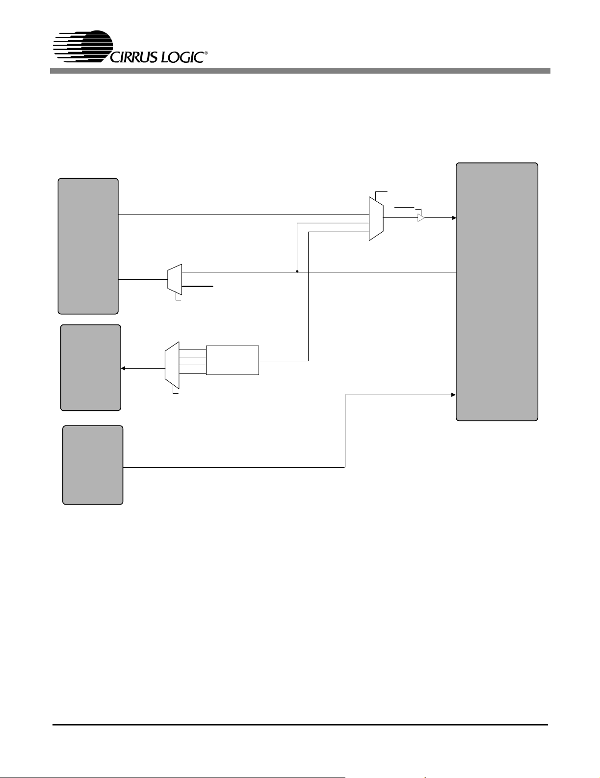
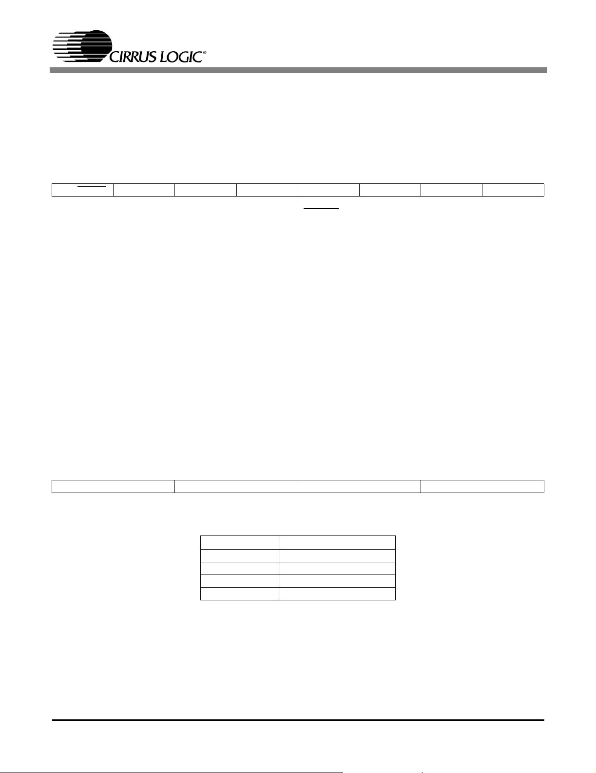
1. SYSTEM OVERVIEW
The CDB42438 evaluation board is an excellent means for evaluating the CS42438 CODEC. Analog and digital audio signal interfaces are provided, an FPGA used for easily configuring the
board and a 9-pin serial cable for use with the supplied Windows® configuration software.
The CDB42438 schematic set has been partitioned into 18 pages and is shown in Figures 8
through 25.
1.1 Power
Power must be supplied to the evaluation board through the +5.0 V, +12.0 V and -12.0 V
binding posts. Jumper J1 connects the VA supply to a fixed +5.0 V or +3.3 V supply. VD, VLS
and VLC are all hard-tied to +3.3 V. All voltage inputs must be referenced to the single black
binding post ground connector (Figure 25 on page 47).
WARNING: Please refer to the CS42438 data sheet for allowable voltage levels.
1.2 Grounding and Power Supply Decoupling
The CS42438 requires careful attention to power supply and grounding arrangements to optimize performance. Figure 8 on page 30 provides an overview of the connections to the
CS42438. Figure 26 on page 48 shows the component placement. Figure 27 on page 49
shows the top layout. Figure 28 on page 50 shows the bottom layout. The decoupling capacitors are located as close to the CS42438 as possible. Extensive use of ground plane fill in
the evaluation board yields large reductions in radiated noise.
1.3 FPGA
See “FPGA System Overview” on page 9 for a complete description of how the FPGA (Figure
12 on page 34) is used on the CDB42438.
1.4 CS42438 Audio CODEC
A complete description of the CS42438 (Figure 8 on page 30) is included in the CS42438
product data sheet.
The required configuration settings of the CS42438 are made in its control port registers, accessible through the “CS42438” tab of the Cirrus Logic FlexGUI software.
Clock and data source selections are made in the control port of the FPGA, accessible
through the “FPGA” tab of the Cirrus Logic FlexGUI software. Refer to registers “CODEC
SDIN Control (address 02h)” on page 16 and “CODEC Clock Control (address 03h)” on
page 17 for configuration settings.
1.5 CS8406 Digital Audio Transmitter
A complete description of the CS8406 transmitter (Figure 11 on page 33) and a discussion
of the digital audio interface are included in the CS8406 data sheet.
The CS8406 converts the PCM data generated by the CS42438 to the standard S/PDIF data
stream. The CS8406 operates in slave mode, accepting either a 128Fs or 256Fs master
4 DS646DB2
Page 5

CDB42438
clock on the OMCK input pin, and can operate in either the Left-Justified or I²S interface format.
Selections are made in the control port of the FPGA, accessible through the “FPGA” tab of
the Cirrus Logic FlexGUI software. Refer to register “CS8406 Control (address 04h)” on
page 17 for configuration settings.
1.6 CS8416 Digital Audio Receiver
A complete description of the CS8416 receiver (Figure 10 on page 32) and a discussion of
the digital audio interface are included in the CS8416 data sheet.
The CS8416 converts the input S/PDIF data stream into PCM data for the CS42438 and operates in master or slave mode, generating either a 128Fs or 256Fs master clock on the
RMCK output pin, and can operate in either the Left-Justified or I²S interface format.
Selections are made in the control port of the FPGA, accessible through the “FPGA” tab of
the Cirrus Logic FlexGUI software. Refer to register “CS8416 Control (address 05h)” on
page 18 for configuration settings.
1.7 CS5341
A complete description of the CS5341 Audio ADC (Figure 20 on page 42) is included in the
CS5341 data sheet.
The CS5341 is connected to the AUX port of the CS42438 and is used only in the TDM interface format of the CODEC. The AUX port of the CS42438 masters the CS5341 and accepts either Left-Justified or I²S data on AUX_SDIN.
Selections are made in the control port of the FPGA, accessible through the “FPGA” tab of
the Cirrus Logic FlexGUI software. Refer to register “CS5341 and Miscellaneous Control (Address 08h)” on page 22 for configuration settings.
1.8 Canned Oscillator
Oscillator Y1 provides a system master clock. This clock is routed through the CS8416 and
out the RMCK pin when the S/PDIF input is disconnected (refer to the CS8416 data sheet for
details on OMCK operation). To use the canned oscillator as the source of the MCLK signal,
remove the S/PDIF input to the CS8416 and configure the CS8416 appropriately.
The oscillator is mounted in pin sockets, allowing easy removal or replacement.The board is
shipped with a 12.2880 MHz crystal oscillator populated at Y1.
1.9 External Control Headers
The evaluation board has been designed to allow interfacing with external systems via the
headers J11 and J24.
The 10-pin, 2 row header, J24, provides access to the serial audio signals required to interface with a DSP (see Figure 9 on page 31).
DS646DB2 5
Page 6

CDB42438
Selections are made in the control port of the FPGA, accessible through the “FPGA” tab of
the Cirrus Logic FlexGUI software. Refer to register “DSP Header Control (address 07h)” on
page 20 for configuration settings
The 12-pin, 3 row header, J11, allows the user bidirectional access to the SPI/I2C control signals by simply removing all the shunt jumpers from the “PC” position. The user may then
choose to connect a ribbon cable to the “EXTERNAL” position. A single “GND” row for the
ribbon cable’s ground connection is provided to maintain signal integrity. Two unpopulated
pull-up resistors are also available should the user choose to use the CDB for the I2C power
rail.
1.10 Analog Input
RCA connectors supply the CS42438 analog inputs through unity gain, AC-coupled singleended to differential circuits. The inputs may also be driven single-ended by shunting the appropriate stake headers labeled “Single In”. A 1 Vrms single-ended signal into the RCA connectors will drive the CS42438 inputs to full scale.
1.11 Analog Outputs
The CS42438 analog outputs may be routed either through a single-pole RC passive filter,
or a differential to single-ended 2-pole active filter.
1.12 Serial Control Port
A graphical user interface is included with the CDB42438 to allow easy manipulation of the
registers in the CS42438 (see the CS42438 data sheet for register descriptions) and FPGA
(see section 5 on page 16 for register descriptions). Connecting a cable to the RS-232 connector (J7) and launching the Cirrus Logic FlexGUI software will enable the CDB42438.
Refer to “Software Mode” on page 7 for a description of the Graphical User Interface (GUI).
1.13 USB Control Port
The USB control port connector (J12) is currently unavailable.
6 DS646DB2
Page 7
CDB42438
2. SOFTWARE MODE
The CDB42438 is shipped with a Microsoft Windows® based GUI, which allows control over the
CS42438 and FPGA registers. Interface to the GUI is provided using an RS-232 serial cable.
Once the appropriate cable is connected between the CDB42438 and the host PC, load “FlexLoader.exe” from the CDB42438 directory. Once loaded, all registers are set to their default reset state. The GUI’s “File” menu provides the ability to save and load script files containing all of
the register settings. Sample script files are provided for basic functionality. Refer to section 3.1
on page 9 for details.
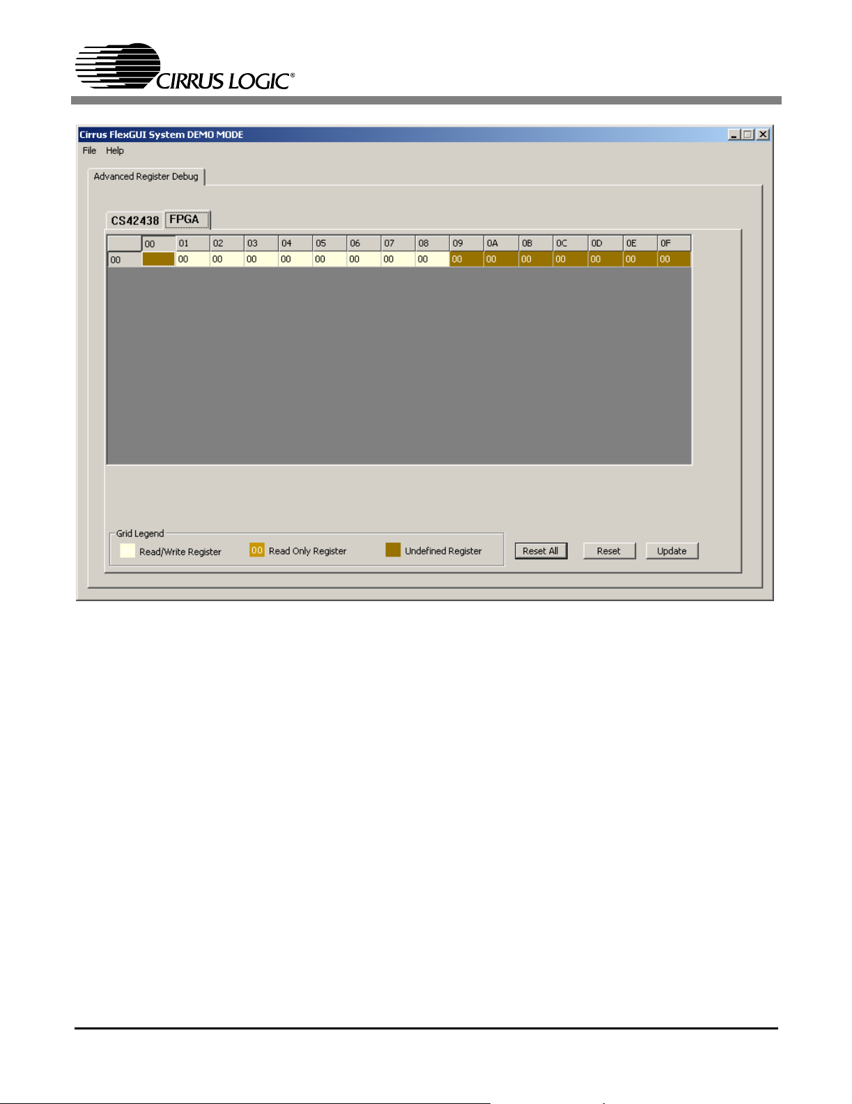
2.1 Advanced Register Debug Tab
The Advanced Register Debug tab provides low level control over the CS42438 and FPGA
individual register settings. Each device is displayed on a separate tab. Register values can
be modified bit-wise or byte-wise. For bit-wise, click the appropriate push button for the desired bit. For byte-wise, the desired hex value can be typed directly in the register address
box in the register map.
Figure 1. Advanced Register Tab - CS42438
DS646DB2 7
Page 8
CDB42438
Figure 2. Advanced Register Tab - FPGA
8 DS646DB2
Page 9

CDB42438
3. FPGA SYSTEM OVERVIEW
The FPGA (U16) controls all digital signal routing between the CS42438, CS8406 CS8416,
CS5341 and the DSP I/O Header. For easy evaluation of the TDM interface format of the
CS42438, the FPGA will copy stereo PCM data from either the CS8416 or DSP I/O Header onto
one data line at a 256Fs data rate. It will in turn de-multiplex the TDM data from the CS42438
and output stereo channel pairs to the CS8406.
3.1 FPGA Setup
Sections 3.2 to 3.4 show graphical descriptions of the routing topology internal to the FPGA.
Section 3.5 shows the graphical description of the FPGA’s control of the MCLK bus. And section 3.6 provides details for routing clocks and data, bypassing the FPGA (recommended for
more advanced users only). Refer to “FPGA Register Description” on page 16 for all configuration settings.
The board may also be configured simply by choosing from 6 pre-defined scripts provided in
the supplied CD ROM. The pre-defined scripts, along with a brief description, are shown below.
3.1.1 S/PDIF In, S/PDIF Out (SPDIF1-4)
This script sets up the CDB42438 to operate the CS8416 as the master and all other devices as slave. The CS8416 masters the MCLK bus.
Various permutations of this option exist as S/PDIF1, S/PDIF2, S/PDIF3 and S/PDIF4.
Each permutation signifies which ADC data is transmitted to the CS8406.
The CS42438 operates in the TDM digital interface format. The FPGA copies PCM data
from the CS8416 onto one data line and transmits this data to the DAC_SDIN input.
3.1.2 Analog In, Analog Out (Digital Loopback)
This script sets up the CDB42438 to operate the crystal oscillator as the master. The
CS8416 passes the signal from the crystal oscillator, Y1, through its OMCK input and out
its RMCK output (NOTE: the S/PDIF input must be disconnected). The CS8416 then generates sub clocks derived from the crystal oscillator and input to the FPGA for TDM clock
generation. The FPGA then masters the sub clocks to the CS42438.
The CS42438 operates in the TDM digital interface format, looping ADC_SDOUT back
into the DAC_SDIN input. ADC1-3 appear on DAC1-3 and the CS5341 ADC appears on
DAC4.
3.1.3 DSP Routing
This script sets up the CDB42438 to operate the device attached to the DSP Header as
the master and all other devices as slave. The DSP Header masters the MCLK bus.
DS646DB2 9
Page 10
CDB42438
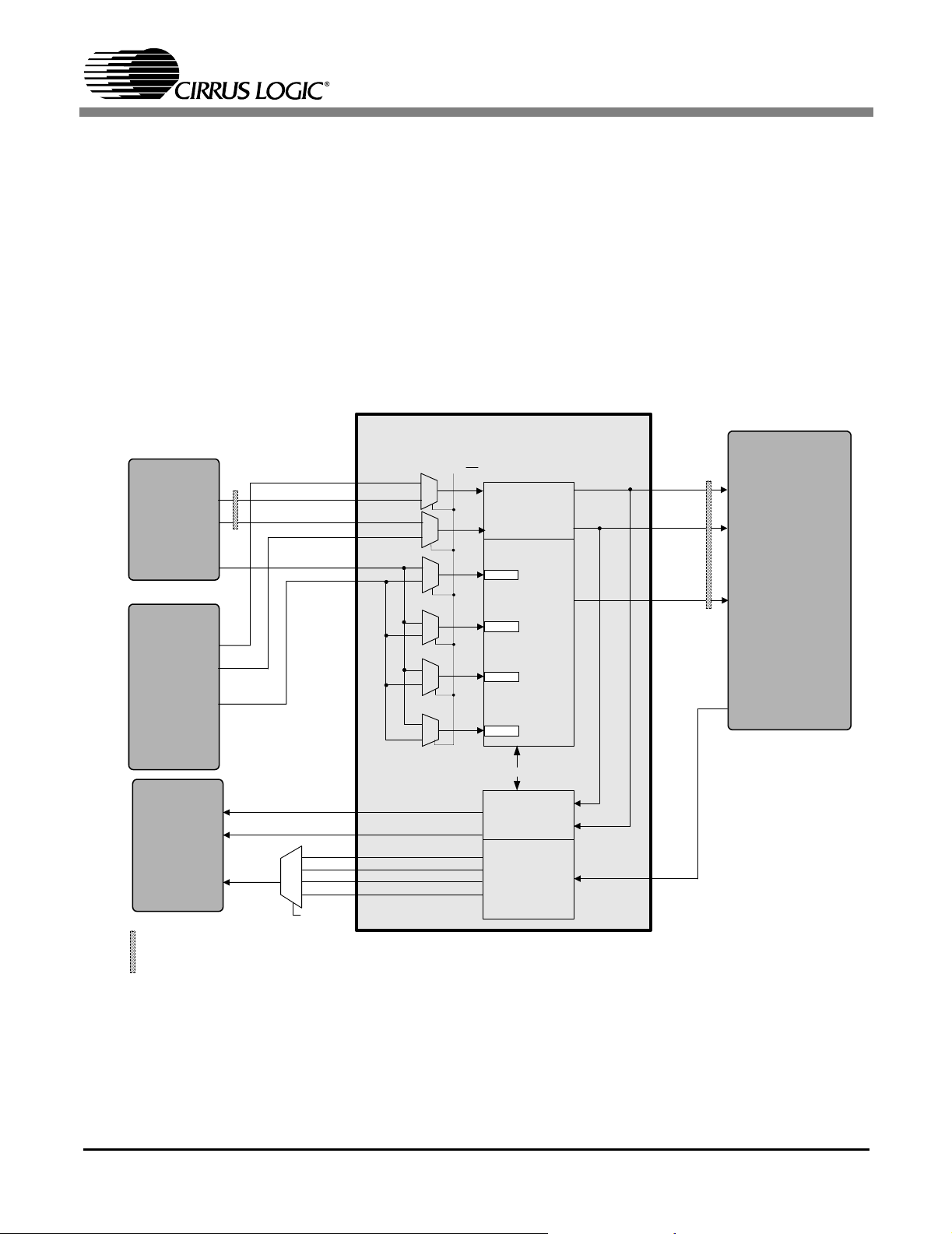
3.2. Internal Sub-Clock Routing
The graphical description below shows the internal clock routing topology between the CS42438,
CS8416, CS8406 and DSP Header. Refer to registers “CODEC Clock Control (address 03h)” on
page 17, “CS8406 Control (address 04h)” on page 17 and “CS8416 Control (address 05h)” on
page 18 for configuration settings.
CS8416
LRCK
SCLK
DSP Header
DSP FS
DSP SCLK
CS8406
LRCK
SCLK
CS8416 LRCK
CS8416 SCLK
DSP_FS
DSP_SCLK
M/S
AUX LRCK
CS42438
AUX SCLK
TDMer
DSP_FS
DSP_SCLK
256Fs
FS
256Fs
CODEC_CLK.MUX[1:0]
FPGA->CODEC
FS
CODEC_CLK.MUX[1:0]
FPGA->CODEC
FS
SCLK
AUX LRCK
AUX_LRCK
AUX SCLK
AUX_SCLK
Figure 3. Internal Sub-Clock Routing
10 DS646DB2
Page 11
CDB42438
3.3. Internal Data Routing
The graphical description below shows the internal data routing topology between the CS42438,
CS8416, CS8406 and DSP Header. Refer to registers “CODEC SDIN Control (address 02h)” on
page 16, “CS8406 Control (address 04h)” on page 17 and “DSP Header Control (address 07h)”
on page 20 for configuration settings.
CS42438
DSP Header
SDIN_MUX[1:0]
DSP_DOUT
DSP_DIN
CS8406
CS8416
SDOUT
SDIN
DATA_MUX[2:0]
ADC1
ADC2
ADC3
AUX
MUX[2:0]
ADC1,2,3, AUX
TDMer
TDM Stream
DSP OUT
SDOUT
TDM Stream
DSPDATA->DAC
SDIN
SDOUT
AUX_SDIN
Figure 4. Internal Data Routing
DS646DB2 11
Page 12
CDB42438
3.4. Internal TDM Conversion, MUXing and Control (TDMer)
The graphical description below shows the routing topology of the TDM converter between the
CS42438, CS8416, CS8406 and DSP Header. Refer to register “TDM Conversion (address
01h)” on page 16 for configuration settings.
The TDMer allows the user to easily evaluate the CS42438 in the TDM digital interface format.
A 256Fs clock and an FS pulse is derived from either the CS8416 or DSP Header. Data is multiplexed onto one data line and transmitted to the DAC. Likewise, data from the ADC of the
CS42438 is de-multiplexed and transmitted to the CS8406.
The TDMer is also capable of transmitting the de-multiplexed data to the DSP Header; however,
the user must re-time this data using a DSP. The CDB42438 does not provide an option for routing the TDM2PCM clocks to the DSP Header.
TDMer
CS42438
CS8416
LRCK
SCLK
DSP_FS
CS8416_LRCK
CS8416_SCLK
DSP_SCLK
DSP/CS8416
PCM2TDM
Clocks
256Fs SCLK
FS
SCLK
FS
SDOUT
CS8416_SDOUT
DSP_DOUT
DSP Header
DSP_FS
DSP_SCLK
DSP_DOUT
CS8406
LRCK
SCLK
SDIN
T2P_LRCK
T2P_SCLK
ADC1
ADC2
ADC3
AUX
D_MUX[2:0]
= Other logic prior to input/output pin of FPGA not shown.
Figure 5. TDMer
Data
SLOT1
SLOT2
SLOT3
SLOT4
MCLK
TDM2PCM
Clocks
Data
TDM Stream
DAC_SDIN
ADC_SDOUT
12 DS646DB2
Page 13
CDB42438
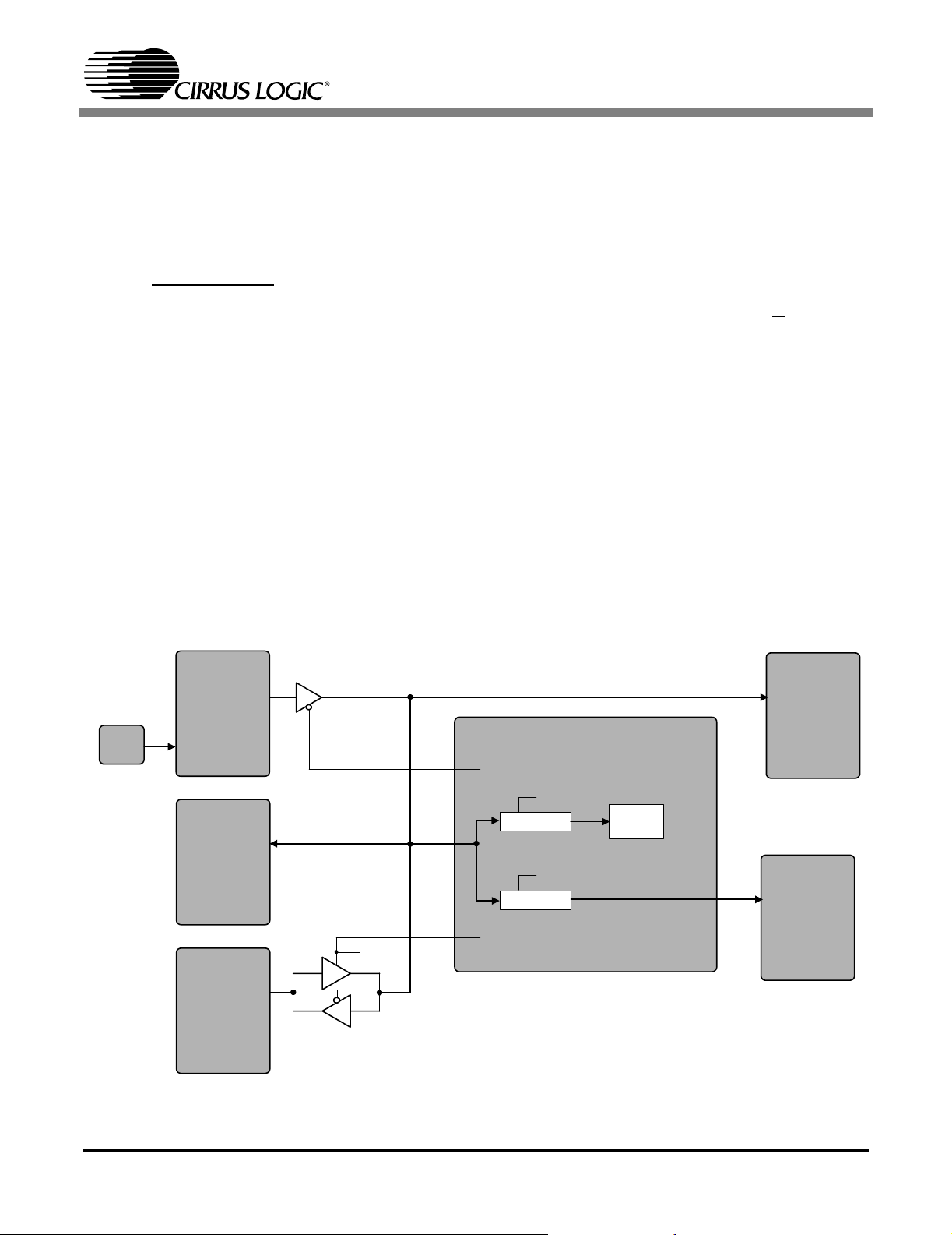
3.5 External MCLK Control
Several sources for MCLK exist on the CDB42438. The crystal oscillator, Y1, will master the
MCLK bus when no S/PDIF signal is input to the CS8416 (refer to the CS8416 data sheet for
details on OMCK operation). This signal will be driven directly out the CS8416.
The CS8416 will generate a master clock whenever its internal PLL is locked to the incoming
S/PDIF stream. This MCLK signal from the CS8416 can be taken off the MCLK bus by setting
the “RMCK_Master” bit in the register “CS8416 Control (address 05h)” on page 18.
The DSP Header can master or slave the MCLK bus by setting the “MCLK_M/S” bit in the
register “DSP Header Control (address 07h)” on page 20 accordingly.
3.5.1 CS5341 MCLK
To accommodate an MCLK signal greater than 25 MHz on the MCLK bus, a 2.0 divider
internal to the FPGA has been implemented. The divided MCLK signal is routed only to
the CS5341. Refer to register “CS5341 and Miscellaneous Control (Address 08h)” on
page 22 for the required setting.
3.5.2 TDMer MCLK
MCLK signals greater than 256Fs must be divided accordingly to maintain a 256Fs MCLK
signal into the TDMer. A 1.5 and a 2.0 divider has been implemented inside the FPGA.
Refer to register “CS5341 and Miscellaneous Control (Address 08h)” on page 22 for the
required setting.
OSC
CS8416
OMCK
CS8406
DSP Header
DSP_MCLK
RMCK
OMCK
RMCK_Master
Reg 05h[0]
Divider
Divider
MCLK_M/S
Reg 07h[0]
FPGA
Reg 08h[6:5]
TDMer
Reg 08h[3:2]
CS42438
MCLK
CS5341
MCLK
Figure 6. External MCLK Control
DS646DB2 13
Page 14

CDB42438
3.6 Bypass Control - Advanced
The DSP clocks and data may be routed through buffers directly to the CS42438, bypassing
the FPGA. This configuration may be desired for more stringent timing requirements at higher
clock speeds. See register “Bypass Control (address 06h)” on page 19. These bits are only
accessible through the Advanced tab of the Cirrus Logic FlexGui software.
Setting “Bypass_FPGA” to ‘0’b will route the DSP sub-clocks directly to the CODEC. “DSPDATA->DAC” and “SDOUT->DSP” should also be set to ‘0’b in bypass mode.
NOTE: To avoid contention with the FPGA, set the cloc k direction for th e FPGA appropriately : The FPGA->CODEC bits in register 03h must be set to ‘1’b.
14 DS646DB2
Page 15
4. FPGA REGISTER QUICK REFERENCE
Function 7 6 5 4 3 2 1 0
TDM Conver-
01h
sion
p16 default
CODEC
02h
SDIN Control
p16 default
CODEC
03h
Clock Control
p17 default
CS8406 Con-
04h
trol
p17 default
CS8416 Con-
05h
trol
p18 default
Bypass Con-
06h
trol
p19 default
DSP Header
07h
Control
p20 default
CS5341/Misc
08h
Control
p22 default
DSP/CS8416 Reserved Reserved Reserved Reserved Reserved Reserved PDN_TDMer
0000000 0
Reserved Reserved Reserved Reserved Reserved Reserved SDIN.MUX1 SDIN.MUX0
1111111 0
Reserved Reserved Reserved Reserved Reserved CLK_MUX1 CLK_MUX0 FPGA->
0011011 0
Reserved Reserved MUX2 MUX1 MUX0 128/256
0110000 1
Reserved Reserved Reserved RST
0011100 0
BypassFPGA
1110111 1
Reserved Reserved DATA_MUX2 DATA_MUX1 DATA_MUX0 Reserved Reserved MCLK_M/S
0000001 0
Reserved Reserved INT.MCLK_
0100000 1
DSPDATA
->DAC
Reserved CS5341
->AUX
DIV
OMCK/DIV_
1.5/2
M/S 128/256 Fs I²S/LJ RMCK_Master
Reserved Reserved Reserved Reserved
‘41_MCLK_
DIV
Fs I²S/LJ Reserved
‘41_DIV_
1.5/2
‘41_I²S/LJ
CDB42438
CODEC
‘41_RST
DS646DB2 15
Page 16
CDB42438
5. FPGA REGISTER DESCRIPTION
All registers are read/write. See the following bit definition tables for bit assignment information. The default state of each bit after a power-up sequence or reset is listed in each bit description.
5.1 TDM CONVERSION (ADDRESS 01H)
76543210
DSP/CS8416 Reserved Reserved Reserved Reserved Reserved Reserved PDN_TDMer
5.1.1 PCM2TDM CLOCK SELECTION (DSP/CS8416)
Default = 0
0 - CS8416
1- DSP Header
Function:
This bit selects the clock source for the PCM2TDM (P2T) converter. It also selects the data source
for Slot 1-4 (see Figure 5 on page 12) of the TDMer.
5.1.2 POWER DOWN TDM CONVERTER (PDN_TDMER)
Default = 0
0 - Disabled
1- Enabled
Function:
This bit powers down the TDMer.
5.2 CODEC SDIN CONTROL (ADDRESS 02H)
76543210
Reserved Reserved Reserved Reserved Reserved Reserved SDIN.MUX1 SDIN.MUX0
5.2.1 SDIN MUX(SDIN.MUX)
Default = 10
SDIN.MUX[1:0] Data Selection
00
01
10
11
Reserved
DSP_DOUT
ADC_SDOUT
TDM Stream
Table 1. Data to SDIN
Function:
This MUX selects the data lines from the DSP Header, the ADC and the TDM Stream from the TDMer
(see Figure 4 on page 11).
16 DS646DB2
Page 17

CDB42438
5.3 CODEC CLOCK CONTROL (ADDRESS 03H)
76543210
Reserved Reserved Reserved Reserved Reserved CLK_MUX1 CLK_MUX0 FPGA->CODEC
5.3.1 MUX (CLK_MUX)
Default = 11
CLK_MUX[1:0] Clock Selection
00
01
10
11
Table 2. Clocks toCODEC
Function:
This MUX selects the sub-clock lines from the DSP Header and the sub-clocks from the TDMer internal to the FPGA (see Figure 3 on page 10).
Reserved
Reserved
DSP
TDMer
5.3.2 FPGA CLOCKS TO CODEC CLOCKS (FPGA->
CODEC)
Default = 0
0 - FPGA Masters CODEC clock bus
1 - FPGA Slave to CODEC clock bus
Function:
This bit toggles a control line for the internal clock buffer to the CODEC ser ial port (see Figur e 3 on
page 10).
5.4 CS8406 CONTROL (ADDRESS 04H)
76543210
Reserved Reserved MUX2 MUX1 MUX0 128/256 Fs I²S/LJ Reserved
5.4.1 DATA MUX(MUX)
Default = 100
MUX[2:0] Data Selection
000
001
010
011
100
101
110
111
Reserved
Reserved
Reserved
Reserved
ADC1 (from ADC_SDOUT)
ADC2 (from ADC_SDOUT)
ADC3 (from ADC_SDOUT)
EXT_ADC (from ADC_SDOUT)
Table 3. Data to CS8406
DS646DB2 17
Page 18

CDB42438
Function:
This MUX selects the data lines from the ADC’s and the external ADC. The last 4 selections are demultiplexed from the TDM stream of SDOUT (see Figure 5 on page 12).
5.4.2 OMCK/LRCK RATIO SELECT (OMCK 128/256
Default = 0
0 - 256 Fs
1 - 128 Fs
Function:
Selects the MCLK/LRCK ratio of the CS8406 transmitter.
5.4.3 LEFT-JUSTIFIED OR I
Default = 0
0 - Left Justified
1 - I
²S
Function:
Selects either I
²S or Left Justified interface format for the CS8406.
²S INTERFACE FORMAT (I²S/LJ)
FS)
5.5 CS8416 CONTROL (ADDRESS 05H)
76543210
Reserved Reserved Reserved RST M/S 128/256 Fs I²S/LJ RMCK_Master
5.5.1 RESET (RST
Default = 1
0 - CS8416 held in reset
1 - CS8416 taken out of reset
Function:
This bit is used to reset the CS8416 and is held low for 300 µs upon FPGA initialization. It is also
pulled low for 300 µs whenever registers 05h[3:1] change.
5.5.2 MASTER/SLAVE SELECT (M/S
Default = 1
0 - Slave
1 - Master
Function:
Selects master/slave mode for the CS8416 and configures the inte rnal routing buffers. Pin 6 (RST
18 DS646DB2
)
)
bit)
Page 19

is held low for 300 µs whenever this bit changes.
CDB42438
5.5.3 RMCK/LRCK RATIO SELECT (128/256
Default = 0
0 - 256 Fs
1 - 128 Fs
Function:
Selects the RMCK/LRCK ratio for the CS8416. Pin 6 (RST
bit changes.
5.5.4 LEFT-JUSTIFIED OR I
Default = 0
0 - Left-Justified
1 - I
²S
Function:
Selects either I
µs whenever this bit changes.
5.5.5 RMCK MASTERS MCLK BUS (RMCK_MASTER
Default = 0
0 - Enabled
1 - Disabled
²S or Left Justified interface format for the CS8416. Pin 6 (RST bit) is held low for 300
²S INTERFACE FORMAT (I²S/LJ)
FS)
bit) is held low for 300 µs whenever this
)
Function:
Enables/disables the external MCLK output buffer on the MCLK bus (see Figure 6 on page 13).
5.6 BYPASS CONTROL (ADDRESS 06H)
76543210
BypassFPGA DSPDATA
->DAC
NOTE: To avoid contention with the FPGA, set the clock direction for the FPGA appropriately: FPGA->CODEC in
register 03h must be set to ‘1’b.
5.6.1 BYPASS FPGA (BYPASSFPGA
Default = 1
0 - Enable
1 - Disable
Function:
This bit toggles a control line for the external data buffer to route the DSP directly to the CODEC.
Reserved CS5341
->AUX
Reserved Reserved Reserved Reserved
)
DS646DB2 19
Page 20

CDB42438
5.6.2 DSP DATA ROUTE TO DAC (DSPDATA->DAC)
Default = 1
0 - Enable
1 - Disable
Function:
This bit toggles a control line for the data buffer external to th e FPGA to route th e DSP Data dir ec tly
to the DAC. The inverted signal controls active low buffers internal to the FPGA that routes the FPGA
data to the DAC. Refer to Figure 4 on page 11.
5.6.3 ADC TO AUX SDIN (CS5341->AUX
)
Default = 0
0 - Enable
1 - Disable
Function:
This bit toggles a control line for the external data buffer to route the external ADC Data directly to the
AUX_SDIN port. When disabled, the FPGA will route the CS8416 SDOUT to the AUX_SDIN port.
5.7 DSP HEADER CONTROL (ADDRESS 07H)
76543 2 1 0
Reserved Reserved DATA_MUX 2 DATA_MUX1 DATA_MUX0 Reserved Reserved MCLK_M/S
5.7.1 DATA MUX(DATA_MUX[2:0])
Default = 000
DSP Data Selection
MUX[2:0] DSP SDIN
000
001
010
011
100
101
110
111
ADC_SDOUT
ADC1 (from ADC_SDOUT)
ADC2 (from ADC_SDOUT)
ADC3 (from ADC_SDOUT)
EXT_ADC (from ADC_SDOUT)
ADC1 (from ADC_SDOUT)
ADC2 (from ADC_SDOUT)
ADC3 (from ADC_SDOUT)
Table 4. Data to DSP
Function:
This MUX selects the data lines from the ADC’s and the external ADC. The first selection shown in
Table 4 comes directly from data output line. The last 7 are de -multiplexed from the TDM data stre am
(NOTE: in this latter scenario, the data will need to be re-timed from the TDMer’s sub clocks). Refer
to Figure 4 on page 11.
20 DS646DB2
Page 21

5.7.2 DSP MCLK (MCLK_M/S)
Default = 0
0 - DSP MCLK is a slave to the MCLK bus.
1 - DSP MCLK masters MCLK bus.
Function:
Enables/disables the external DSP MCLK output buffer on the MCLK bus.
CDB42438
DS646DB2 21
Page 22

CDB42438
5.8 CS5341 AND MISCELLANEOUS CONTROL (ADDRESS 08H)
76543210
Reserved Reserved INT.MCLK_
DIV
5.8.1 INT MCLK DIVIDE (1.5/2.0 DIVIDE)
Default = 0
0 - Disabled
1 - Enabled
Function:
Enables/disables the internal (1.5 or 2.0) divide circuitry for MCLK.
5.8.2 1.5 OR 2.0 MCLK DIVIDE (1.5/2.0 DIVIDE)
Default = 0
0 - Divide by 1.5
1 - Divide by 2.0
INT.DIV_
1.5/2
‘41_MCLK_
DIV
‘41_DIV_
1.5/2
‘41_I²S/LJ ‘41_RST
Function:
Divides the internal MCLK by 1.5 or 2 to all internal logic. This is intended to accommodate an external
MCLK that is greater than 256 Fs. SCLK is derived from MCLK and must always be 256Fs in TDM
Mode (see Figure 6 on page 13).
5.8.3 EXT MCLK DIVIDE (‘41_MCLK_DIV)
Default = 0
0 - Disabled
1 - Enabled
Function:
Enables/disables the internal (1.5 or 2.0) divide circuitry for the CS5341 MCLK.
5.8.4 1.5 OR 2.0 CS5341 MCLK DIVIDE (‘41_DIV_1.5/2.0)
Default = 0
0 - Divide by 1.5
1 - Divide by 2.0
Function:
Divides the MCLK from the MCLK bus to the CS5341 by 1.5 or 2 (see Figure 6 on page 13).
5.8.5 LEFT-JUSTIFIED OR I
²S INTERFACE FORMAT (‘41_I²S/LJ)
Default = 0
0 - Left Justified
1 - I
²S
22 DS646DB2
Page 23

Function:
CDB42438
Selects either I
5.8.6 RESET (‘41_RST
Default = 1
0 - CS5341 is held in reset
1 - CS5341 is taken out of reset
Function:
This bit toggles pin 30 of the FPGA and is held low for 300 µs upon FPGA initialization. It will also be
held low for 300 µs whenever register 08h[1] changes.
²S or Left Justified interface format for the CS5341. Reset to the CS5341 is toggled.
)
DS646DB2 23
Page 24

CDB42438
6. HARDWARE MODE
Switch S1 configures the CDB42438 in hardware mode. Switch S5 sets up the FPGA and controls the routing of all clocks and data. Refer to section 6.1 for a list of the various hardware mode
options available. After setting any of these switches, the user may need to assert a reset by
pressing the “RESET” button (S4) or the “PROGRAM” button (S2) .
6.1 Setup Options
The setup options below allow the user to configure the CDB42438 when the CS42438 is in
hardware mode. The FPGA registers are programmed with the values shown in the table below.
Register
SW[3:0] General Description
0
0000 TDMer w/CS8416 Data (S/PDIF1)
1) CS8416 Masters MCLK & PCM Subclocks
2) CS8416 data duplicated and Time-Division
Multiplexed into DAC SDIN.
3) ADC1 (AIN1-2) de-multiplexed from
SDOUT1 and input into CS8406.
1
0001 TDMer w/CS8416 Data (S/PDIF2)
1) CS8416 Masters MCLK & PCM Subclocks
2) CS8416 data duplicated and Time-Division
Multiplexed into DAC_SDIN.
3) ADC2 (AIN3-4) de-multiplexed from
ADC_SDOUT and input into CS8406.
2
0010 TDMer w/CS8416 Data (S/PDIF3)
1) CS8416 Masters MCLK & PCM Subclocks
2) CS8416 data duplicated and Time-Division
Multiplexed into DAC_SDIN.
3) ADC3 (AIN5-6) de-multiplexed from
ADC_SDOUT and input into CS8406.
Address Value Detail Description
01h 00h TDM Conversion - CS8416 clocks & data to TDMer.
02h 03h SDIN Control - TDMer output data input to SDIN.
03h 36h CODEC Clock Control - CODEC slave to TDMer.
04h 61h CS8406 Control - ADC1 to CS8406.
05h 38h CS8416 Control - CS8416 masters MCLK bus and
provides PCM subclocks to the TDMer.
06h EFh Bypass Control - N/A.
07h 02h DSP Header - DSP Slave to MCLK.
08h 41h CS5341/Misc. Control - N/A.
01h 00h TDM Conversion - CS8416 clocks & data to TDMer.
02h 03h SDIN Control - TDMer output data input to SDIN.
03h 36h CODEC Clock Control - CODEC slave to TDMer.
04h 69h CS8406 Control - ADC2 to CS8406.
05h 38h CS8416 Control - CS8416 masters MCLK bus and
provides PCM subclocks to the TDMer.
06h EFh Bypass Control - N/A.
07h 02h DSP Header - DSP Slave to MCLK.
08h 41h CS5341/Misc. Control - N/A.
01h 00h TDM Conversion - CS8416 clocks & data to TDMer.
02h 03h SDIN Control - TDMer output data input to SDIN.
03h 36h CODEC Clock Control - CODEC slave to TDMer.
04h 71h CS8406 Control - ADC3 to CS8406.
05h 38h CS8416 Control - CS8416 masters MCLK bus and
provides PCM subclocks to the TDMer.
06h EFh Bypass Control - N/A.
07h 02h DSP Header - DSP Slave to MCLK.
08h 41h CS5341/Misc. Control - N/A.
24 DS646DB2
Page 25

Register
SW[3:0] General Description
3
0011 TDMer w/CS8416 Data (S/PDIF4)
4
0100 Reserved
5
0101 Reserved
6
0110 Reserved
7
0111 Reserved
8
1000 Reserved
9
1001 Reserved
10
1010 DSP Routing
11
1011 FPGA Bypass w/DSP MCLK
12
1100 Reserved
13
1101 Reserved
14
1110 Reserved
1) CS8416 Masters MCLK & PCM Subclocks
2) CS8416 data duplicated and Time-Division
Multiplexed into DAC_SDIN.
3) External ADC (AUX1-2) de-multiplexed
from ADC_SDOUT and input into CS8406.
1) DSP Masters MCLK & TDM Subclocks
(through FPGA).
1) DSP Masters MCLK & TDM Subclocks
(bypassing FPGA).
Address Value Detail Description
CDB42438
01h 00h TDM Conversion - CS8416 clocks & data to TDMer.
02h 03h SDIN Control - TDMer output data input to SDIN.
03h 36h CODEC Clock Control - CODEC slave to TDMer.
04h 79h CS8406 Control - AUX to CS8406.
05h 38h CS8416 Control - CS8416 masters MCLK bus and
provides PCM subclocks to the TDMer.
06h EFh Bypass Control - N/A.
07h 02h DSP Header - DSP Slave to MCLK.
08h 41h CS5341/Misc. Control - N/A.
01h 01h TDM Conversion - TDMer powered down.
02h 01h SDIN Control - DSP data input to DAC_SDIN.
03h 24h CODEC Clock Control - CODEC slave to DSP.
04h 61h CS8406 Control - N/A.
05h 29h CS8416 Control - N/A.
06h EFh Bypass Control - N/A.
07h 07h DSP Header Control - DSP Masters MCLK.
08h 41h CS5341 Control - N/A.
01h F0h TDM Conversion - N/A.
02h 00h SDIN Control - N/A.
03h 09h CODEC Clock Control - N/A.
04h 01h CS8406 Control - N/A.
05h 29h CS8416 Control - N/A.
06h 0Ch Bypass Control - DSP to CODEC.
07h 07h Misc. Control - DSP Master.
08h 41h CS5341 Control - Left-justified data from CS5341.
Maximum MCLK = 25 MHz.
DS646DB2 25
Page 26

SW[3:0] General Description
15
1111 TDMer w/Digital Loopback
1) Oscillator Y1 Masters MCLK passed
through CS8416. [REMOVE S/PDIF INPUT]
2) ADC SDOUT into DAC SDIN.
CDB42438
Register
Address Value Detail Description
01h 00h TDM Conversion - CS8416 clocks & data to TDMer.
02h FEh SDIN Control - ADC_SDOUT input to DAC_SDIN.
03h 36h CODEC Clock Control - CODEC slave to TDMer.
04h 61h CS8406 Control - N/A
05h 38h CS8416 Control - Oscillator Y1 masters MCLK
passed through CS8416 to MCLK bus and CS8416
provides PCM subclocks to the TDMer. [S/PDIF
input must be removed]
06h EFh Bypass Control - N/A.
07h 08h Misc. Control - DSP Slave to MCLK.
08h 41h CS5341 Control - Left-justified data from CS5341.
Maximum MCLK = 25 MHz.
26 DS646DB2
Page 27

7. CDB CONNECTORS AND JUMPERS
Reference
CONNECTOR
+5V J2 Input
+12V J5 Input
-12V J4 Input
GND J3 Input
SPDIF OPTICAL OUT J14 Output
SPDIF COAX OUT J18 Output
SPDIF OPTICAL IN J21 Input
SPDIF COAX IN J25 Input
RS232 J7 Input/Output
USB J12 Input/Output
DSP Header J24 Input/Output
CONTROL J11 Input/Output
USB JTAG J8 Input/Output
FPGA JTAG J10 Input/Output
USB RESET S1 Input
FPGA RESET S2 Input
AIN1
AIN2
AIN3
AIN4
AIN5-/5B
AIN5+/5A
AIN6-/6B
AIN6+/6A
AIN7
AIN8
AOUT1
AOUT2
AOUT3
AOUT4
AOUT5
AOUT6
AOUT7
AOUT8
Designator INPUT/OUTPUT SIGNAL PRESENT
J37
J27
J23
J17
J15
J13
J9
J6
J28
J38
J47
J48
J49
J50
J51
J52
J53
J54
Input
Input
Output
Table 5. System Connections
CDB42438
+5.0 V Power Supply
+12.0 V Power Supply
-12.0 V Power Supply
Ground Reference
CS8406 digital audio output via optical cable
CS8406 digital audio output via coaxial cable
CS8416 digital audio input via optical cable
CS8416 digital audio input via coaxial cable
Serial connection to PC for SPI / I2C control port signals
USB connection to PC for SPI / I2C control port signals.
Not Available.
I/O for Clocks & Data
I/O for external SPI / I2C control port signals.
I/O for programming the micro controller (U9).
I/O for programming the FPGA (U16).
Reset for the micro controller (U9).
Reset for the FPGA (U16).
RCA phono jacks for analog input signal to CS42438.
RCA phono jacks for analog input signal to CS5341.
RCA phono jacks for analog outputs.
DS646DB2 27
Page 28

JUMPER PURPOSE POSITION FUNCTION SELECTED
J1 Selects source of voltage for the VA supply +3.3V
AIN1-
(J26)
AIN2-
(J22)
AIN3-
(J19)
AIN4-
(J16)
J29-J36
J39-J46
Selects the negative leg of the single-ended to
differential input circuit in differential mode, or a
VA/2 bias in single-ended mode.
Selects the negative leg of the single-ended to
differential input circuit in differential mode, or a
VA/2 bias in single-ended mode.
Selects the negative leg of the single-ended to
differential input circuit in differential mode, or a
VA/2 bias in single-ended mode.
Selects the negative leg of the single-ended to
differential input circuit in differential mode, or a
VA/2 bias in single-ended mode.
Selects between an active or a passive analog
output filter for AOUT1-8.
SINGLE IN
SINGLE IN
SINGLE IN
SINGLE IN
Table 6. Jumper Settings
*+5V
*DIFF IN
*DIFF IN
*DIFF IN
*DIFF IN
*A
P
Voltage source is +3.3 V regulator
Voltage source is +5 V regulator
Inverted signal from AIN1 input
VA/2 voltage bias
Inverted signal from AIN2 input
VA/2 voltage bias
Inverted signal from AIN3 input
VA/2 voltage bias
Inverted signal from AIN4 input
VA/2 voltage bias
2-Pole Active Filter
Single-Pole Passive Filter
CDB42438
*Default factory settings
28 DS646DB2
Page 29

8. CDB BLOCK DIAGRAM
CDB42438
Single-Ended
Output
Differential Input
Input
Power
Figure 25 on page 47
ANALOG INPUT
y Single-Ended to
C/SPI Header
2
I
Figure 19 on page 41
Figure 16 on page 38 to
y Single-Ended
ANALOG OUTPUT
y Differential to
30
Output
y Single-Ended
Figure 24 on page 46
Figure 21 on page 43 to
AUXILIARY
ANALOG INPUT
y Single-Ended
Input
Figure 20 on page 42
42
CS5341
Figure 8 on page
Serial Control Port
Figure 14 on page 36 to Figure 15 on page 37
CS42438
Data
Clocks/
MCLK Divided
Figure 20 on page
Figure 7. Block Diagram
Control
Hardware
Clocks & Data
FPGA
Figure 13 on page 35
Figure 12 on page 34 to
/Data
Clocks
Input
32
Figure 10 on page
Osc.
DSP HEADER
Figure 9 on page 31
S/PDIF
Output
CS8406
MCLK BUS
Clocks/Data
33
Figure 11 on page
Setup
Hardware
S/PDIF
CS8416
DS646DB2 29
Page 30

9. CDB SCHEMATICS
CDB42438
Figure 8. CS42438
30 DS646DB2
Page 31

CDB42438
Figure 9. DSP Header
DS646DB2 31
Page 32

CDB42438
Figure 10. S/PDIF Input
32 DS646DB2
Page 33

CDB42438
Figure 11. S/PDIF Output
DS646DB2 33
Page 34

CDB42438
Figure 12. FPGA
34 DS646DB2
Page 35

CDB42438
Figure 13. FPGA Connections
DS646DB2 35
Page 36

CDB42438
Figure 14. Control Port
36 DS646DB2
Page 37

CDB42438
Figure 15. Control Port Connections
DS646DB2 37
Page 38

CDB42438
Figure 16. Analog Input 1-2
38 DS646DB2
Page 39

CDB42438
Figure 17. Analog Input 3-4
DS646DB2 39
Page 40

CDB42438
Figure 18. Analog Input 5
40 DS646DB2
Page 41

CDB42438
Figure 19. Analog Input 6
DS646DB2 41
Page 42

CDB42438
Figure 20. Analog Input 7-8
42 DS646DB2
Page 43

CDB42438
Figure 21. Analog Output 1-2
DS646DB2 43
Page 44

CDB42438
Figure 22. Analog Output 3-4
44 DS646DB2
Page 45

CDB42438
Figure 23. Analog Output 5-6
DS646DB2 45
Page 46

CDB42438
Figure 24. Analog Output 7-8
46 DS646DB2
Page 47

CDB42438
Figure 25. Power
DS646DB2 47
Page 48

10.CDB LAYOUT
CDB42438
Figure 26. Silk Screen
48 DS646DB2
Page 49

CDB42438
Figure 27. Top side Layer
DS646DB2 49
Page 50

CDB42438
Figure 28. Bottom side Layer
50 DS646DB2
Page 51

11.REVISION HISTORY
Revision Date Changes
DB1 July 2004 Initial Release
DB2 OCT 2004 Removed Bill of Materials
Schematic Changes: Changed R224, R226, R228, R230 , R234, R235, R236,
R237 from 6.19 kΩ to 4.75 kΩ on Figure 21 on page 43, Figure 22 on page 44,
Figure 23 on page 45, Figure 24 on page 46.
Layer Changes: Corrected silk screen lables for S1, J8, J11, and J24 on Fig-
ure 26 on page 48. Changed bottom layer lot number on Figure 28 on p a ge 50.
Table 7. Revision History
CDB42438
Contacting Cirrus Logic Support
For all product questions and inquiries contact a Cirrus Logic Sales Representative.
To find one nearest you go to www.cirrus.com
IIMPORTANT NOTICE
Cirrus Logic, Inc. and i ts s ub sidi ar ies ( “Ci rru s” ) be li e ve that the in fo rma tio n con tai ne d in t his do cu ment is a ccu ra te a nd r eliable. However, the infor-
mation is subject to change without notice and is provided “AS IS” without warranty of any kind (express or implied). Customers are advised to obtain
the latest version of rel evant informat ion to verif y, before pl acing order s, that info rmation being relied on is c urrent and c omplete. Al l products are
sold subject to the terms and condition s of sale supplied at the time of order ackn owledgment, incl uding those pe rtaining to warrant y, patent infring ement, and limitation of liability. No responsib ility is ass umed by Cirru s for the use of this infor mation, in cludin g use of this information as the basis for
manufacture or sale of any items, or for infringement of patents or other rights of third parties. This document is the property of Cirrus and by furnishing
this information, Cirrus grant s no license, express o r implied under any pat ents, mask work rights, copyrights, trademar ks, trade secrets or other
intellectual property rights. Cirrus owns the copyrights associated with the i nformation contained herein and gives consent for copies to be made of
the information only for use within your organization with respect to Cirrus integrated circuits or other parts of Cirrus. This consent does not extend
to other copying such as copyin g for general distribution, advertising or promotional purposes, or for creating any work for resale.
CERTAIN APPLICATIONS USING SEMICONDUCTOR PRODUCTS MAY INVOLVE POTENTIAL RISKS OF DEATH, PERSONA L INJURY, OR
SEVERE PROPERTY OR ENVIRONMENTAL DAMAGE ("CRITICAL APPLICATIONS "). CIRRUS PRODUCTS ARE NOT DESIGNED, AUTHORIZED OR WARRANTED FOR USE IN AIRCRAFT SYSTEMS, MILITARY APPLICATIONS, PRODUCTS SURGICALLY IMPLANTED INTO THE
BODY, LIFE SUPPORT PRODUCTS OR OTHER CRITICAL APPLICATIONS (INCLUDING MEDICAL DEVICES, AIRCRAFT SYSTEMS OR COMPONENTS AND PERSONAL OR AUTOMOTIVE SAFETY OR SECURITY DEVICES). INCLUSION OF CIRRUS PRODUCTS IN SUCH APPLICATIONS IS UNDERSTOOD TO BE FULLY AT THE CUSTOMER'S RISK AND CIRRUS DISCLAIMS AND MAKES NO WARRANTY, EXPRESS,
STATUTORY OR IMPLIED, INCLUDING THE IMPLIED WARRANTIE S OF MERCHANTABILITY AND FITNES S FOR PARTICULAR PURPOSE,
WITH REGARD TO ANY CIRRUS PRODUCT THAT IS USED IN SUCH A MANNER. IF THE CUSTOMER OR CUSTOMER'S CUSTOMER USES
OR PERMITS THE USE OF CIRRUS PRODUCTS IN CRITICAL APPLICATIONS, CUSTOMER AGREES, BY SUCH USE, TO FULLY INDEMNIFY
CIRRUS, ITS OFFICERS, DIRECTORS, EMPLOYEES, DISTRIBUTORS AND OTHER AGENTS FROM ANY AND ALL LIABILITY, INCLUDING
ATTORNEYS' FEES AND COSTS, THAT MAY RESULT FROM OR ARISE IN CONNECTION WITH THESE USES.
I²C is a registered tradem ar k of P hilip s S em ico nduc tor. Pu rch ase o f I²C co mp onen ts of C irrus Log ic, Inc ., or o ne of its sub lice nsed Associated Companies conveys a license under the Phillips I²C Patent Rights to use those components in a standard I²C system.
Cirrus Logic, Cirrus, the Ci rrus Logic logo des igns, and PopGua rd are trademarks of Cirrus Logic, Inc. All other b rand and product names in this
document may be trademarks or serv ice marks of their respective owners.
Windows® is a registered trademark of Micros oft Corporation.
DS646DB2 51
 Loading...