

Page 1
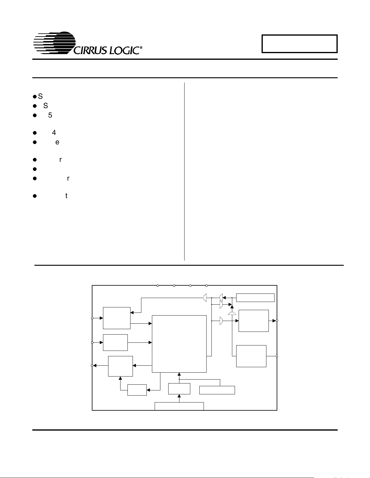
Evaluation Board For CS424xx
CDB42428
Features
Single-Ended Analog Inputs and Outputs
CS8416 S/PDIF Receiver
CS5361 converters supply ADCIN1 and
ADCIN2 for CS424xx One Line Modes
CS8406 S/PDIF Digital Audio Transmitter
Header for optional external configuration of
CS424xx and board
Header for external DSP serial audio I/O
3.3 or 5.0 Volt Logic Interface supply
Demonstrates recommended layout and
grounding arrangements
Microsoft Windows® compatible software
interface to configure CS424xx and interboard connections
I
Description
The CDB42428 demonstration board is an excellent
means for evaluating the CS424xx family of highly integrated multi-channel CODECs. Evaluation requires an
analog/digital signal source and analyzer, Windows®
compatible computer, and power supplies.
System timing can be provided by an on-board oscillator
or a master clock recovered from the S/PDIF input to the
CS8416. RCA phono jacks are provided for the CS5361
analog inputs and CS424xx analog inputs and outputs.
Digital data I/O is available via RCA phono jacks or optical connectors to the CS8416 and from the CS8406.
The Windows® software provides a graphical user interface to make configuration of the board easy. The
software communicates through the computer’s parallel
port, and will configure the hardware to allow all features
of the CS424xx to be evaluated. The evaluation board
may also be configured to accept external timing and
data signals for operation in a user application during
system development.
ORDERING INFORMATION
CDB42428 Evaluation Board
Ana log Inputs
Ana log Inputs
Analog O utputs
Cirrus Logic, Inc.
http://www.cirrus.com
CS5361
(x2)
Analog
Filter
8-ch
Analog
Output
Mute
+18V -18V +5V GND
C S 42428
CPLD
PC Parallel Port
Copyright Cirrus Logic, Inc. 2003
(All Rights Reserved)
Ext. Control
DSP Header
CS8406
CS8416
S/PDIF Output
S/PDIF Input
Nov ‘03
DS605DB1
1
Page 2

TABLE OF CONTENTS
1. SYSTEM OVERVIEW ...............................................................................................................4
1.1 CS424xx ............................................................................................................................ 4
1.2 CS8406 .............................................................................................................................. 4
1.3 CS8416 .............................................................................................................................. 4
1.4 CS5361 .............................................................................................................................. 4
1.5 Crystal Oscillator ................................................................................................................ 4
1.6 Analog Input ....................................................................................................................... 4
1.7 Analog Outputs .................................................................................................................. 4
1.8 CPLD ................................................................................................................................. 6
1.9 DB-25 Computer Parallel Port ...........................................................................................6
1.10 External Control Header .................................................................................................. 6
1.11 DSP Header ..................................................................................................................... 6
1.12 LED Function Indicator ....................................................................................................6
1.13 Power ............................................................................................................................... 6
1.14 Grounding and Power Supply Decoupling ....................................................................... 6
1.15 External Control Header Signals ...................................................................................... 7
1.16 DSP Header Signals ........................................................................................................9
2. INITIAL BOARD SETUP .........................................................................................................10
2.1 Power Supplies: ............................................................................................................... 10
2.2 Installing the Software: ..................................................................................................... 10
3. CDB425XX.EXE USER'S GUIDE ........................................................................................... 11
3.1 Main Window ................................................................................................................... 11
3.2 CS42428 Window ............................................................................................................ 11
3.3 Preset Scripts ................................................................................................................... 11
3.4 Quick Start Preset - Analog In to Analog Out ..................................................................11
3.5 Quick Start Preset - Analog In to Digital Out ....................................................................11
3.6 Quick Start Guide - Digital In to Analog Out .................................................................... 12
3.7 Quick Start Preset - One-Line Mode (OLM) ..................................................................... 13
4. MUTING SCHEME ................................................................................................................. 14
5. SCHEMATICS AND LAYOUT ........................................................................................... 15
6. ADDENDUM ...........................................................................................................................32
CDB42428
LIST OF FIGURES
Figure 1. Instrumentation Amplifier Configuration ........................................................................... 5
Figure 2. Output Channel Mute Select ..........................................................................................14
Figure 3. CS424xx......................................................................................................................... 15
Figure 4. Clocks, Data, and DSP Header ...................................................................................... 16
Figure 5. SPDIF............................................................................................................................. 17
Figure 6. CS5361 External ADC #1 .............................................................................................. 18
Figure 7. CS5361 External ADC #2 .............................................................................................. 19
Figure 8. CS424xx Analog Inputs.................................................................................................. 20
Figure 9. Analog Outputs A1 and B1............................................................................................. 21
Figure 10. Analog Outputs A2 and B2........................................................................................... 22
Figure 11. Analog Outputs A3 and B3........................................................................................... 23
Figure 12. Analog Outputs A4 and B4........................................................................................... 24
Figure 13. DB-25, Ext Ctrl Header, Reset .....................................................................................25
Figure 14. CPLD............................................................................................................................ 26
Figure 15. Power ...........................................................................................................................27
Figure 16. CS8416 ........................................................................................................................ 28
Figure 17. Component Placement and Reference Designators ....................................................29
2
Page 3

Figure 18. Top Layer..................................................................................................................... 30
Figure 19. Bottom Layer................................................................................................................ 31
LIST OF TABLES
Table 1. System Connections ......................................................................................................... 6
Table 2. Jumper Settings................................................................................................................ 7
Table 3. CS424xx External Control Header Signals ....................................................................... 7
Table 4. CS424xx DSP Header Signals.......................................................................................... 9
CDB42428
3
Page 4

CDB42428
1. SYSTEM OVERVIEW
The CDB42428 demonstration board is an excellent means for evaluating the CS42428/26/18/16 family of highly
integrated CODECs. Analog and digital audio signal interfaces are provided, as well as a DB-25 computer parallel
port interface for use with the supplied Windows® configuration software.
The CDB42428 schematic set has been partitioned into 14 pages as shown in Figures 3 through 16.
1.1 CS424xx
A complete description of each member of the CS42428/26/18/16 family is included in each respective product data
sheet.
1.2 CS8406
The CS8406 S/PDIF transmitter on the demonstration board (see Figure 5) allows the performance of the CS424xx
internal ADC’s to be measured digitally. Either the CS424xx DAC port or the ADC port can be multiplexed to the
CS8406. The CS8406 transmitter is configured to operate in slave mode only, and will receive the required clocks
from the CS424xx. The data format for the CS8406 is selectable and must match that of its source. The CS8406
must be configured using the supplied software.
1.3 CS8416
The CS8416 S/PDIF receiver on the demonstration board (see Figure 5) allows the performance of the CS42428
internal DAC’s to be evaluated through the use of a digital (S/PDIF) input source. The CS8416 receiver interfaces
with the DSP header and can be configured to master the CS424xx DAC and ADC as well as the CS8406. The data
format is selectable and must match that of the CS424xx. The CS8416 must be configured using the supplied software.
1.4 CS5361
There are two CS5361 A/D converters on the CS424xx demonstration board (see Figures 6 and 7). These converters supply the CS424xx ADCIN signals, and must operate in left-justified, 24-bit mode only. Their serial data outputs
are used when supporting the CS424xx One Line Mode of operation.
RCA analog connectors supply the inputs to each CS5361 channel through a unity gain, AC-coupled, single-todif ferential circuit. Each CS5361 input circuit is biased to 1/2 VA, and a 1V
scale. The CS5361 converters are set to operate in slave mode and will receive their clocks from the CS424xx. The
SCLK and LRCK signals can be provided from either the CS424xx DAC or ADC port, and must be selected using
the configuration software.
signal will drive the converter to full
RMS
1.5 Crystal Oscillator
Oscillator Y1 (see Figure 4) provides the System Clock (OMCK) for the CS424xx. The crystal oscillator on the board
is mounted in pin sockets that allow it to be removed or replaced. The board is shipped with a 24.576 MHz crystal
oscillator stuffed at Y1. Please refer to the CS424xx data sheet for details on OMCK operation.
The buffer on the output of the oscillator provides for signal level shifting to the proper VLS supply. This buffer can
be removed if the oscillator is powered from the same VLS voltage source as the codec.
Oscillator Y2 provides the OMCK clock for the CS8416. Please refer to the CS8416 data sheet for details on automatic clock switching operation.This oscillator is not populated.
1.6 Analog Input
RCA phono connectors supply the CS424xx analog inputs through unity gain, AC-coupled single-to-differential circuits (see Figure 8). Each input circuit is biased to match the 2.7V
the CS424xx converter to full scale.
VQ, and a 1V
DC
differential signal will drive
RMS
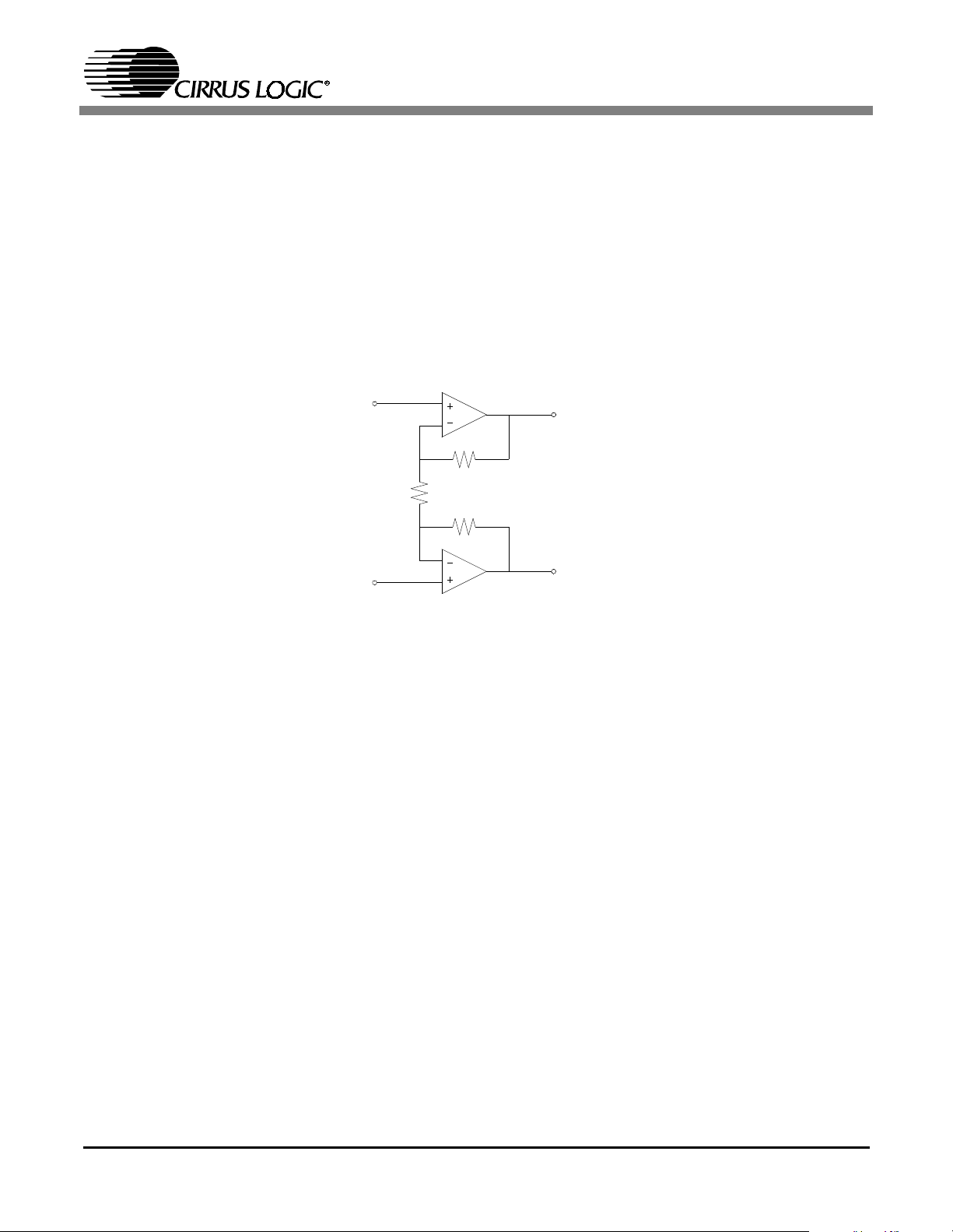
1.7 Analog Outputs
Each CS424xx analog output is routed through a differential to single-ended, unity-gain low pass filter, which is ACcoupled to an RCA phono jack (see Figures 9 through 12). The analog output filter on the CDB42428 has been designed to add flexibility when evaluating the CS424xx DAC outputs. The output filter was designed in a two stage
format, with the first stage being an optional instrumentation amplifier, and the second stage a 2-pole butterworth
low pass filter.
4
Page 5
CDB42428
The 2-pole low pass filter provides an example of an inexpensive circuit with good distortion and dynamic range performance. It is designed to have the in-band impedance matched between the positive and negative legs. It also
provides a balanced to single-ended conversion for standard un-balanced outputs. Evaluate this circuit by placing
the FILT jumpers (three per output channel) to position 1 (selectable by J9, J10 & J11 for OUTA1, etc.).
The instrumentation amplifier is optionally inserted before the LPF by changing the FILT jumpers to position 2. The
instrumentation amplifier incorporates a 5x gain (+14dB) which effectively lowers the noise contribution of the following 2-pole LPF. This improves the overall dynamic range of the system. The gain of this stage is determined from
the following equation:
Gain 1
The resistor designated by R
feedback resistors on the two sides of the instrumentation amp ‘R’ must be equal.
(see Figure 1) can be adjusted to change the gain of the instrumentation amp. The
2
2R()
------------+=
R
2
IN+
R
R2
R
IN-
Figure 1. Instrumentation Amplifier Configuration
A resistor divider pad (parallel combination of R59 // R56 // R80 and R93 for AOUTA1) has been placed after the
low pass filter to bring the circuit back to unity gain (selectable with jumper J12 for AOUTA1).
In the resistor divider pad, three 3.01 kΩ, 1/4 W, 1210 size resistors are used in parallel to provide a combined resistance of 1 kΩ and a combined power handling of 3/ 4W. This is done to provide sufficient power handling capability to accommodate the high signal levels output from the instrumentation amplifier stage. When not using the
instrumentation amplifier, these resistors may be reduced to a single 1kΩ, 1/10 W, 0805 size resistor (for muting
attenuation purposes).
In certain places throughout the output circuit, 1 /8W, 1206 size and 1/4W, 1210 size resistors are used. Similar to
the parallel resistors in the resistor divider pad, these are used to provide sufficient power handling capability in order
to accommodate the high signal levels output from the instrumentation amplifier stage. When not using the instrumentation amplifier, these resistors may all be replaced with 1/ 10W, 0805 size resistors.
The attenuation provided by the output mute transistor (Q2 for OUTA1) is determined by the resistor-divider formed
between the collector-emitter on-resistance and the output resistor of the LPF. The greater the output resistor, the
greater the attenuation will be for a given transistor. The trade off is that a high output impedance is not usually desirable, and may affect the voltage transfer to the next stage based upon its input impedance.
The same resistor that affects the transistor mute level also affects the HPF formed with the output DC-block capacitor (C71 for OUTA1). For LPF configuration 2, the values for the DC-block capacitor and output resistor pad were
chosen to give uniform distortion performance across the audio bandwidth, particularly at low frequency. The HPF
formed by this R-C pair must be such that the voltage across the aluminum electrolytic DC-block capacitor must be
a minimum at 20 Hz. This keeps the distortion due to the electrolytic's dielectric absorption properties to a minimum.
For a design utilizing only LPF configuration 1, there is no post-LPF resistor-divider pad, and a much smaller value
capacitor can be used.
OUT+
OUT-
5
Page 6
CDB42428
1.8 CPLD
The CPLD controls the on-board signal routing and configuration (see Figure 14). The CPLD interfaces with the
computer software through the DB-25 parallel port header, or can communicate with an external processor via the
External Control header.
1.9 DB-25 Computer Parallel Port
On-board clock and data routing and configuration logic, as well as the CS424xx part are configured using a computer with the supplied Windows®-based software. The software communicates via the DB-25 parallel port interface
(see Figure 13) to a local CPLD that can configure all parts on the board.
1.10 External Control Header
A 26-pin dual-row header allows access to the control signals needed to configure the CS424xx. The external controller has access to the CS424xx I
able (see Figure 13). All control header signals are buffered, and are referenced to VLC levels. See Table 3 for a
complete description of External Control Header signals.
1.11 DSP Header
A 32-pin dual-row header provides access to the serial audio signals required to interface with a DSP (see Figure 4).
Either the CS42428 (using the PLL recovered from the input ADC_LRCK or the OMCK oscillator), the CS8416 or
the DSP header can be the master of the MCLK signal. The CS8416 can supply the DSP header with its recovered
master clock (RMCK), or pass the local oscillator-sourced OMCK (of the CS8416).
The CS424xx ADC and DAC ports are individually selectable to be master or slave, and should source/receive their
clocks to/from the DSP as required. All serial port timings must be synchronous to the CS424xx OMCK or RMCK whichever is used to clock the codec. See the data sheet for a complete description of serial port modes of operation.
All DSP header signals are buffered, and are referenced to VLS levels. DSP interface power VLS and ground are
supplied to the header. See Table 4 for a complete description of DSP Header signals.
2
C/SPI signals, master mute and reset, and the CS424xx interrupt signal is avail-
1.12 LED Function Indicator
D1 (see Figure 13) indicates that a master reset condition has occurred on the board. D4 (see Figure 14) is sourced
from the CPLD and is currently unsupported.
1.13 Power
Power can easily be supplied to the evaluation board through three binding posts, all referenced to the single black
binding post ground connector (see Figure 15).
Supply +18.0 VDC to the green binding post to provide the positive analog rail. Supply -18.0 VDC to the yellow binding post to provide the negative analog rail. +18 V and -18 V supply power to the op-amps and can be +/-12 to +/18 volts (must be +/-18 V when filter 2 is selected).
Supply +5.0 VDC to the red binding post. This directly supplies the digital +5 V, is regulated down to provide the
digital +3.3 V, and is filtered to supply VLC, and VA.
VLS and VD must be individually set with jumpers to either +3.3 V or +5 V.
1.14 Grounding and Power Supply Decoupling
The CS424xx requires careful attention to power supply and grounding arrangements to optimize performance.
Figures 18 and 19 detail the routing and component placement for both top and bottom layers of the demonstration
board. Power supply decoupling capacitors are located as close to the CS424xx as possible. Extensive use of
ground plane fill in the demonstration board yields large reductions in radiated noise.
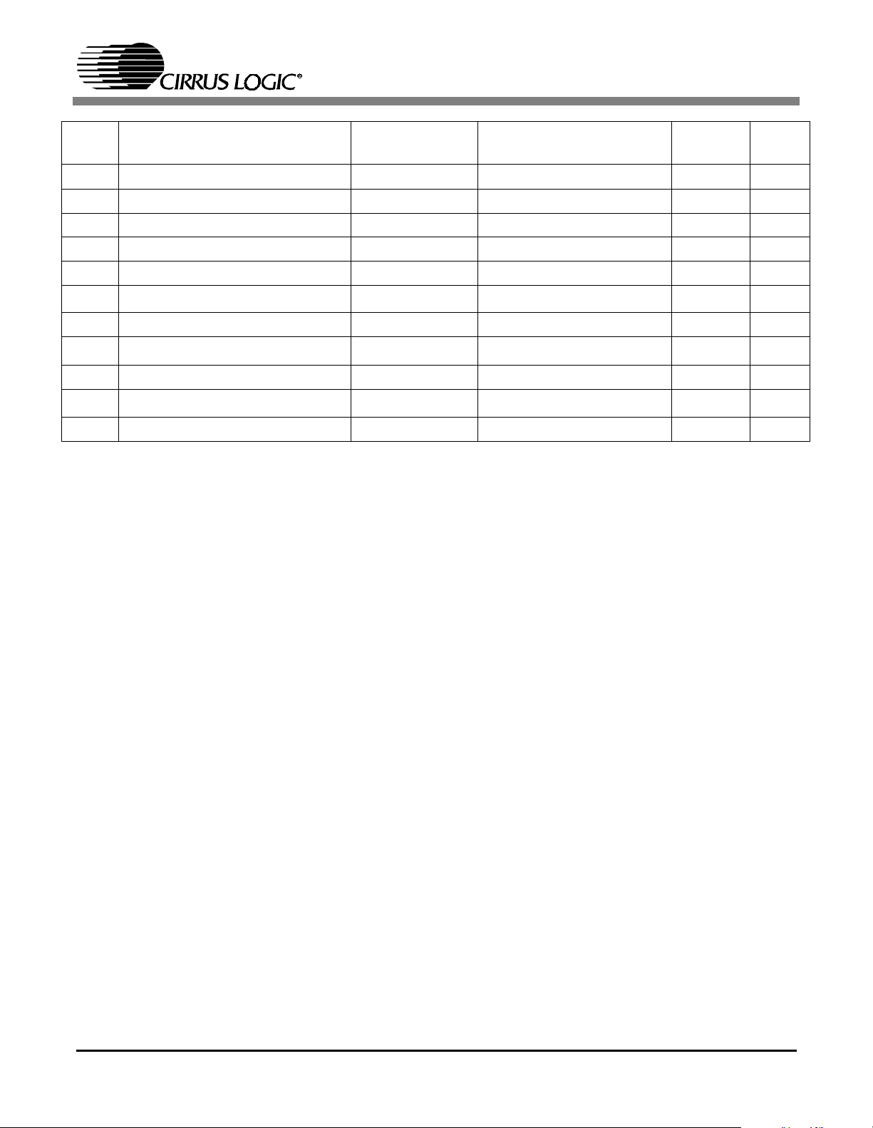
CONNECTOR INPUT/OUTPUT SIGNAL PRESENT
+5V Input + 5VDC power
-18V Input -18 to -12 VDC negative supply for the op-amps
+18V Input +12 to +18 VDC positive supply for the op-amps
GND Input Ground connection from power supply
J39 Input CS8416 digital audio interface input via coax
Table 1. System Connections
6
Page 7
CDB42428
OPT4 Input CS8416 digital audio interface input via optical
SPDIF TX - J2 Output CS8406 digital audio interface output via coax
SPDIF TX - OPT2 Output CS8406 digital audio interface output via optical
PC Port - J22 Input/Output
EXTERNAL CONTROL
Input/Output
Parallel connection to computer for SPI / I
2
I/O for SPI / I
C control port signals - see signal descriptions below
HEADER - J17
DSP HEADER - J36 Input/Output I/O for DSP serial port signals - see signal descriptions below
ANALOG IN LFT/RT Input
RCA phono jacks for analog input signal to CS424xx internal ADCs
EXT A/D #1 LEFT/RIGHT Input RCA phono jacks for analog input signal to CS5361 ADC #1
EXT A/D #2 LEFT/RIGHT Input RCA phono jacks for analog input signal to CS5361 ADC #2
OUT_A1 to OUT_B4 Output RCA phono jacks for channels A1 to B4 analog outputs
Table 1. System Connections
JUMPER / SWITCH PURPOSE POSITION FUNCTION SELECTED
J37 Selects source of voltage for the
VLS supplies
J38 Selects source of voltage for the
VD supply
S2 Stand-Alone Mode Select SAM0
J9,J10,J11
DAC Output Filter select - FILT *1
+3.3 V
*+5 V
+3.3 V
*+5 V
SAM1
Voltage source is +3.3 V regulator
Voltage source is +5 V binding post
Voltage source is +3.3 V regulator
Voltage source is +5 V binding post
Stand-Alone Modes are for debug use
and are presently unsupported
Selects standard 2-pole LPF
J13,J15,J16
J18,J19,J20
2
Selects instrumentation-amp/LPF/pad
J23,J25,J26
J28,J29,J30
J32,J34,J35
J39,J40,J41
J43,J45,J46
*Default Factory Settings
2
C control port signals
Table 2. Jumper Settings
1.15 External Control Header Signals
Header
Pin #
1 External Control Present Signal CTRL EXT_CONTROL_PRESENT- - -
2 Ground CDB GND - -
3
Address Bit 0 (I
4 Ground CDB GND - -
5
Address Bit 1 (I
6 Ground CDB GND - -
7
SDA (I
8 Ground CDB GND - -
9 Serial Control Port Clock CTRL SCL/CCLK 74VHC125 VLC
Signal Description Source Schematic Signal Name Buffer Buffer
2
C) / CS- (SPI)
2
C) / CDIN (SPI)
2
C) / CDOUT (SPI)
CTRL AD0/CS 74VHC125 VLC
CTRL AD1/CDIN 74VHC125 VLC
CTRL or CS424xx
SDA/CDOUT MOSFET VLC
Table 3. CS424xx External Control Header Signals
Vol t a ge
7
Page 8
CDB42428
Header
Pin #
10 Ground CDB GND - -
11 Master MUTE to all Outputs CTRL EXT_MUTE 74VHC125 VLC
12 Ground CDB GND - -
13 Master RESET CTRL EXT_RESET Diode -
14 Ground CDB GND - -
15
CS424xx Interrupt (Programmable) CS424xx
16 Ground CDB GND - -
17
Enable external I
18 Ground CDB GND - -
19
Enable external I
20 Ground CDB GND - -
Signal Description Source Schematic Signal Name Buffer Buffer
EXT_HDR_INT 74VHC125 VLC
2
C interface
2
C interface
Table 3. CS424xx External Control Header Signals (Continued)
CTRL EXT_EN_SCL 74VHC125 VLS
CTRL EXT_EN_SDA 74VHC125 VLS
Vol t a ge
8
Page 9
1.16 DSP Header Signals
CDB42428
Header
Pin #
1 Master Clock
2 Ground CDB GND - -
3 DAC port LRCK
4 Ground CDB GND - -
5 DAC port SCLK
6 Ground CDB GND - -
7 DAC port SDATA Input 1 DSP DSP_SDAT1 74VHC125 VLS
8 Ground CDB GND - -
9 DAC port SDATA Input 2 DSP DSP_SDAT2 74VHC125 VLS
10 Ground CDB GND - -
11 DAC port SDATA Input 3 DSP DSP_SDAT3 74VHC125 VLS
12 Ground CDB GND - -
13 DAC port SDATA Input 4 DSP DSP_SDAT4 74VHC125 VLS
14 Ground CDB GND - -
15 no connect - - - -
16 Ground CDB GND - -
Signal Description Source Schematic
Signal Name
CS424xx or DSP
CS424xx or DSP
CS424xx or DSP
DSP_MCLK 74VHC125 VLS
DSP_DAC_LRCK 74VHC125 VLS
DSP_DAC_SCLK 74VHC125 VLS
Buffer Buffer
Vol t a ge
17 ADC port LRCK
18 Ground CDB GND - -
19 ADC port SCLK
20 Ground CDB GND - -
21 no connect - - - -
22 Ground CDB GND - -
23 ADC port SDATA Output
24 Ground CDB GND - -
25 Unused Buffered Output
26 Ground CDB GND - -
27 No Connect - - - -
28 Ground CDB GND - -
29 Serial Port Interface Power CDB VLS - -
30 Ground CDB GND - -
31 Serial Port Interface Power CDB VLS - -
32 Ground CDB GND - -
Table 4. CS424xx DS P Header Signals
CS424xx or DSP
CS424xx or DSP
CS424xx
-
DSP_ADC_LRCK 74VHC125 VLS
DSP_ADC_SCLK 74VHC125 VLS
DSP_ADC_SDOUT 74VHC125 VLS
- 74VHC125 VLS
9
Page 10

CDB42428
2. INITIAL BOARD SETUP
2.1 Power Supplies:
1) Verify that all power supplies are off before making connections.
2) Connect a +5.0 VDC power supply to the +5 V (J48) red binding post. Select VLS and VD operating voltage by
placing a jumper on J37 and J38 to select either +5 V or +3.3 V.
3) Connect a +12.0 to +18.0 VDC power supply to the +18 V (J50) green binding post. If using the FILT position
number 2 for the output filter stage, then supply +18.0 V only.
4) Connect a -12.0 to -18.0 VDC power supply to the -18 V (J51) yellow binding post. If using the FILT position
number 2 for the output filter stage, then supply -18.0 V only.
5) Connect the common ground of the power supplies to the GND (J49) binding post.
6) Attach parallel port cable between board and computer.
7) Attach all required analog and digital cables to the board jacks and connectors.
8) If using the DSP Header connection, attach the required user supplied flat ribbon cable to the header with the
power supplies turned off.
9) If using the External Control Header connection, attach the required user supplied flat ribbon cable to the header
with the power supplies turned off. Note that external controller must ground the EXT_CONTROL_PRESENTsignal to gain control of the I
1 and 2 together.
10) With all cables and connections in place, turn on the power supplies to the board. Turn on supplies in this order:
+5 V, +18 V, -18 V.
11) Press and release the MASTER RESET switch S1. The LED, D1, will illuminate as long as S1 is depressed indicating a reset condition. Once S1 is released, the LED should turn off. If it remains on, an error has occurred.
At this point, power off the power supplies and re-check all connections. Apply power to the board and press
and release S1. Once the LED has turned off, the board should now be ready for setup and use.
2
C/SPI signals. This can be done easily by connecting External Control Header pins
2.2 Installing the Software:
1) Copy the “CDB GUI” folder and all of its contents from the included CD to a convenient location on your PC.
2) If desired, create a shortcut to CDB425xx.EXE on your desktop. You should now be able to run CDB425xx.EXE.
Double-click on CDB425xx.EXE or its shortcut. Note that the software will configure itself to operate with a
CDB424xx depending upon which is connected to the parallel port.
3) Select the LPT port you are using to connect to the CDB42428.
4) Shut down the application, reset the board, and then restart the application.
10
Page 11

CDB42428
3. CDB425XX.EXE USER'S GUIDE
3.1 Main Window
The main window of the CDB42428 control application allows the user to configure the CDB42428 inter-board routing of clocks and data, as well as setup the CS5361, CS8416 and CS8406 parts. To make changes to the CS5361,
CS8406, CS8416, or inter-board routing, the “Configure Board” radio button must be selected.
The RESET CS425xx button will reset only the part. The MASTER RESET button will reset the CS424xx, as well
as reset the board into its default state.
3.2 CS42428 Window
To configure the CS424xx, the “Configure CS424xx” radio button must be selected, then press the “CS424xx” button. This will bring up the complete CS424xx configuration window.
3.3 Preset Scripts
To make configuring the board and part easier, preset scripts can be saved and recalled. A preset script is a “snapshot” of all GUI board and component settings. This can done using the File pulldown menu and choosing Load or
Save. Scripts are saved with the default .LVS extension, and when loaded, will create a .LOG file. There are several
preset scripts included with the software. The following sections represent four common setup modes with scripts
for quick evaluation of the board.
3.4 Quick Start Preset - Analog In to Analog Out
To measure analog in to analog out performance, you will need the following:
• CS424xx Demonstration Board
• +18 VDC, -18 VDC, and +5 VDC power supplies
• Analog signal source and analyzer
• Windows® compatible computer with parallel port cable and CDB425xx software
Step 1 - Follow Initial Board Setup procedure as described above
Step 2 - Select Output Filter Jumpers
Set all CDB42428 analog output filter jumpers to the FILT2 settings.
Step 3 - Connect to Windows® Software
Connect the computer to the board and launch the CDB425xx software.
Step 4 - Connect Signal Source
Connect the analog output from the analyzer to the Left Analog Input J7. Connect J11 analog OUTA1 RCA to the
input of the analyzer. Set the analyzer output to 1.0 VRMS, 1 kHz. Set the analyzer input to measure signal level
and apply a 22 Hz-22 kHz filter.
Step 5 - Configure the Board
Using the Windows® software, load the preset script “Single Speed Analog In To Analog Out.LVS”. This preset will
configure the CS424xx to use OMCK as the master clock, DAC and ADC ports will be masters, and the
ADC_SDOUT data will source all DAC_SDIN inputs. The left/right analog inputs will appear at all odd/even analog
outputs. The single speed sample rate will be 48 kHz based upon the 24.576 MHz OMCK. You may load the similar
double speed or quad speed presets to investigate higher sample rates.
Step 6 - Measure Audio
You should now have audio appearing at the Analog A1 output.
3.5 Quick Start Preset - Analog In to Digital Out
To measure the analog to digital converter performance, you will need the following:
• CS424xx Demonstration Board
• +18 VDC, -18 VDC, and +5 VDC power supplies
11
Page 12

CDB42428
• Analog signal source and analyzer
• Digital signal source and analyzer
• Windows® compatible computer with parallel port cable and CDB425xx software
Step 1 - Follow Initial Board Setup procedure as described above
Step 2 - Connect to Windows® Software
Connect the computer to the board and launch the CDB425xx software.
Step 3 - Connect Signal Source
Connect the analog output from the analyzer to the Left Analog Input J7. Connect the CS8406 digital output (coax
J2 or optical OPT2) to the input of the analyzer. Set the analyzer output to 1.0 VRMS, 1 kHz. Set the analyzer input
to measure digital signal level and apply a 22 Hz-22 kHz filter.
Step 4 - Configure the Board
Using the Windows® software, load the preset script “Single Speed Analog In To Digital Out.LVS”. This preset will
configure the CS424xx to use OMCK as the master clock, DAC and ADC ports will be masters, and the ADC clocks
data will source the CS8406 inputs. The CS8406 will output the ADC digital data to both the optical and RCA jacks.
The single speed sample rate will be 48 kHz based upon the 24.576 MHz OMCK. You may load the similar double
speed or quad speed presets to investigate higher sample rates.
Step 5 - Measure Audio
You should now have digital audio appearing at the ADC_SDOUT port and the CS8406 digital output.
3.6 Quick Start Guide - Digital In to Analog Out
To measure digital to analog performance, you will need the following:
• CS424xx Demonstration Board
• +18 VDC, -18 VDC, and +5 VDC power supplies
• Analog signal source and analyzer
• Digital signal source and analyzer
• Windows® compatible computer with parallel port cable and CDB425xx software
Step 1 - Follow Initial Board Setup procedure as described above
Step 2 - Select Output Filter Jumpers
Set all CDB42428 analog output filter jumpers to the FILT2 settings.
Step 3 - Connect to Windows® Software
Connect the computer to the board and launch the CDB425xx software.
Step 4 - Connect Signal Source
Connect the S/PDIF digital output from the analyzer to the optical input connector OPT4. Connect the analog OUTA1
RCA phono jack J11 to the input of the analyzer. Set the analyzer output to 0 dBFS, 1 kHz, sample rate at 48 kHz.
Set the analyzer input to measure signal level and apply a 22 Hz-22 kHz filter.
Step 5 - Configure the Board
Using the Windows® software, load the preset script “Single Speed Optical In to Analog Out.LVS”. This preset will
configure the CS8416 to source all DAC_SDIN inputs. The test source left/right data will appear at all odd/even analog outputs. You may load the similar double speed or quad speed presets to investigate higher sample rates, but
you must be sure to supply an appropriate speed SPDIF signal.
Step 6 - Measure Audio
You should now have audio appearing at the Analog A1 output.
12
Page 13

CDB42428
3.7 Quick Start Preset - One-Line Mode (OLM)
To measure one-line mode analog in to analog out performance, you will need the following:
• CS424xx Demonstration Board
• +18 VDC, -18 VDC, and +5 VDC power supplies
• Analog signal source and analyzer
• Windows® compatible computer with parallel port cable and CDB425xx software
Step 1 - Follow Initial Board Setup procedure as described above
Step 2 - Select Output Filter Jumpers
Set all CDB42428 analog output filter jumpers to the FILT2 settings.
Step 3 - Connect to Windows® Software
Connect the computer to the board and launch the CDB425xx software.
Step 4 - Connect Signal Source
Connect the analog output from the analyzer to the Left Analog Input J7. Connect J11 analog OUTA1 RCA to the
input of the analyzer. Set the analyzer output to 1.0 VRMS, 1 kHz. Set the analyzer input to measure signal level
and apply a 22 Hz-22 kHz filter.
Step 5 - Configure the Board
Using the Windows® software, load the preset script “One-Line Mode.LVS”. This preset will configure the CS424xx
to use OMCK as the master clock, DAC and ADC ports will be masters, and the ADC_SDOUT data will source the
DAC_SDIN1 input. The left/right analog inputs will appear at OUT_A1 and OUT_B1 analog outputs; the
EXT_ADC#1 Left and Right inputs will appear on the OUT_A2 and OUT_B2 analog outputs, respectively; the
EXT_ADC#2 Left and Right inputs will appear on the OUT_A3 and OUT_B3 analog outputs, respectively. The sample rate will be 48 kHz based upon the 24.576 MHz OMCK.
Step 6 - Measure Audio
You should now have audio appearing at the Analog outputs.
13
Page 14

4. MUTING SCHEME
CDB42428
CHANNEL
MUTE CONTROL
1
and MUTEC
EXT_MUTE
and MUTEC
EXT_MUTE
2
or
and GPO7
EXT_MUTE
and MUTEC
EXT_MUTE
3 - 8
or
and GPO6
EXT_MUTE
MUTE CH 1
MUTE CH 2
+V
MUTEC
EXT_MUTE
EN_MUTE7
GPO7
Figure 2. Output Channel Mute Select
MUTEC
MUTE CH 3 - 8
MUTEC
EN_MUTE6
GPO6
14
Page 15

5. SCHEMATICS AND LAYOUT
CDB42428
Figure 3. CS424xx
15
Page 16

CDB42428
16
Figure 4. Clocks, Data, and DSP Header
Page 17

CDB42428
Figure 5. SPDIF
17
Page 18

CDB42428
18
Figure 6. CS5361 External ADC #1
Page 19

CDB42428
Figure 7. CS5361 External ADC #2
19
Page 20

CDB42428
20
Figure 8. CS424xx Analog Inputs
Page 21

CDB42428
Figure 9. Analog Outputs A1 and B1
21
Page 22

CDB42428
22
Figure 10. Analog Outputs A2 and B2
Page 23

CDB42428
Figure 11. Analog Outputs A3 and B3
23
Page 24

CDB42428
24
Figure 12. Analog Outputs A4 and B4
Page 25

CDB42428
Figure 13. DB-25, Ext Ctrl Header, Reset
25
Page 26

CDB42428
Figure 14. CPLD
26
Page 27

CDB42428
Figure 15. Power
27
Page 28

CDB42428
Figure 16. CS8416
28
Page 29

CDB42428
Figure 17. Component Placement and Reference Designators
29
Page 30

CDB42428
Figure 18. Top Layer
30
Page 31

CDB42428
Figure 19. Bottom Layer
31
Page 32

CDB42428
6. ADDENDUM
The following silkscreen markings on the evaluation board are mislabeled and should be labeled as specified (all
schematic labels in Figures 3-16 are correct):
1) DSP HEADER pin 23 (DAC_SDOUT) should be labeled “DSP_ADC_SDOUT”.
2) DSP HEADER pin 25 (ADC_SDOUT) should be labeled “DSPHDR_PIN25”.
3) Test point ADC_SDOUT should be labeled “U27_PIN54”.
4) Test point DAC_SDOUT should be labeled “ADC_SDOUT”.
Contacting Cirrus Logic Support
For all product questions and inquiries contact a Cirrus Logic Sales Representative.
To find one nearest you go to www.cirrus.com
IMPORTANT NOTICE
Cirrus Logic, Inc. and its subsidiaries ("Cirrus") believe that the information contained in this document is accurate and reliable. Ho wever, the information is subject to change without notice and is provided "AS IS" without warranty of any kind (expres s or implied) . Cust omers are advised to obtain the latest version of
relevant information to verify, before placing orders, that information being relied on is current and complete. All products are sold subject to the te rms and conditions of sale supplied at the time of order acknowledgment, including those pertaining to warranty, patent infringement, and limita tion of li a bility. N o responsibility is assum ed by C irrus fo r the u se o f this information , includ in g us e of this infor m ation as the basis for man ufacture or sale of any items, or for infringement
of patents or other rights of third parties. This document is the property of Cirrus and by furnishing this information, Cirr us grants no licens e, expres s or implied
under any patents, mask work rights, copyrights, trademarks, trade secrets or other intellectual property rights. Cirrus owns th e copyrights associated with the
information contained herein and gives consent for copies to be made of the information only for use within your organization wi th respec t to C irru s i ntegrated
circuits or other products of Cirrus. This consent does not extend to other copying such as copying for general distribution, advertising or promotional purposes,
or for creating any work for resale.
An export permit needs to be obtained from the competent authorities of the Japanese Government if any of the products or technologies described in this material and controlled under the "Foreign Exchange and Foreign Trade Law" is to be exported or taken out of Japan. An export license and/or quota needs to be
obtained from the competent authorities of the Chinese Government if any of the products or technologies described in this material is subject to t he PRC Foreign
Trade Law and is to be exported or taken out of the PRC.
CERTAIN APPLICATIONS USING SEMICONDUCTOR PRODUCTS MAY INVOLVE POTENTIAL RISKS OF DEATH, PERSONAL INJURY, OR SEVERE
PROPERTY OR ENVIRONMENTAL DAMAGE ("CRITICAL APPLICATIONS"). CIRRUS PRODUCTS ARE NOT DESIGNED, AUTHORIZED OR WARRANTED FOR USE IN AIRCRAFT SYSTEMS, MILITARY APPLICATIONS, PRODUCTS SURGICALLY IMPLANTED INTO THE BODY, LIFE SUPPORT PRODUCTS
OR OTHER CRITICAL APPLICATIONS (INCLUDING MEDICAL DEVICES, AIRCRAFT SYSTEMS OR COMPONENTS AND PERSONAL OR AUTOMOTIVE
SAFETY OR SECURITY DEVICES). INCLUSION OF CIRRUS PRODUCTS IN SUCH APPLICATIONS IS UNDERSTOOD TO BE FULLY AT THE CUSTOMER'S RISK AND CIRRUS DISCLAIMS AND MAKES NO WA RRA NTY, EXPRESS, STATUTOR Y OR IMPLIED, INCLUDING THE IMPLIED WARRANTIES OF
MERCHANTABILITY AND FITNESS FOR PARTICULAR PURPOSE, WITH REGARD TO ANY CIRRUS PRODUCT THAT IS USED IN SUCH A MANNER. IF
THE CUSTOMER OR CUSTOMER'S CUSTOMER USES OR PERMITS THE USE OF CIRRUS PRODUCTS IN CRITICAL APPLICATIONS, CUSTOMER
AGREES, BY SUCH USE, TO FULLY INDEMNIFY CIRRUS, ITS OFFICERS, DIRECTORS, EMPLOYEES, DISTRIBUTORS AND OTHER AGENTS FROM
ANY AND ALL LIABILI TY, INCLUDING ATTORNEYS' FEES AND COSTS, THAT MAY RESULT FROM OR ARISE IN CONNECTION WITH THESE USES.
Cirrus Logic, Cirrus, and the Cirrus Logic logo designs are trademarks of Cirrus Logic, Inc. All other brand and product names in this document may be trademarks or service marks of their respective owners.
I2C is a registered trademark of Philips Semiconductor. Purchase of I2C Components of Cirrus Logic, Inc., or one of its sublicensed Associated Companies
conveys a license under the Philips I2C Patent Rights to use those components in a standard I2C system.
Microsoft Windows is a registered trademark of Microsoft Corporation.
32
 Loading...