

Page 1
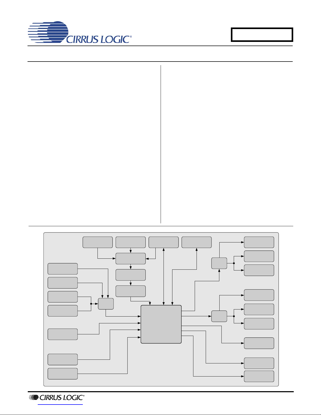
CS4207
Lineout 1
Stereo
MI CIN Mo n o
MI CIN St ereo
Line In Stereo
Lineout 2
Stereo
Lineout 2
Balanced Left
Lineout 2
Balanced Right
*these connect or s have pr esence det e ct ion
Headphone
Output
Optical
S/PDIF In
Optical
S/PDIF Out 1
Optical
S/PDIF Out 2
HD Audio Bus
Headers
CS4207 GPI O
Header
CS4207
Supplies
Regulators
Current Sense
Resistors
Digita l M i c
Headers
External Bench
Supplies
PC Peripheral
Power
Jumper
Select
MICIN Balanced
Left
MICIN Balanced
Right
Jumper
Select
Lineout 1
Balanced Left
Lineout 1
Balanced Right
Jumper
Select
*
*
*
*
*
CDB4207
CS4207 HD Audio CODEC Development Platform
Features
Demonstrates Recommended Layout and
Grounding Arrangements
Analog I/O Use Standard 1/8” (3.5 mm) or 1/4”
(6.35 mm) Jacks With Presence Detection
Analog Inputs (Passive)
– Single-ended and Differential MIC Inputs
– Single-ended Stereo Line-level Input
Analog Outputs (Passive)
– Stereo Headphone Output with Test Loads
– Single-ended and Differential Line Outputs
Digital I/O
– Optical S/PDIF I/O Jacks
– Digital MIC Input Headers
– HD Audio Bus Headers
– CS4207 GPIO Header
Powered by HDA Bus Connection to PC
– Optionally Powered by Bench Supply or PC
Peripheral Power Supply Cable (Molex)
Configured by Hardware Jumpers
– Power Supply Sources, Analog I/O Settings
Current Sense Resistors for CS4207 Supplies
Description
The CDB4207 is a flexible development platform designed for easy evaluation of the CS4207 HD Audio
CODEC. Evaluation requires a PC with an HD Audio
Bus connector and an analog or digital audio signal
source for recording. Analog I/O is provided via 1/8” or
1/4” jacks. S/PDIF I/O is provided via optical connectors. Two identical HD Audio Bus headers are provided
for connection to a PC.
The CDB4207 is configured via hardware jumper settings to set up the analog I/O circuitry and select a
source for each CS4207 power supply rail. The analog
inputs and outputs support several signal types for compatibility with a variety of signal sources and analyzers.
The CS4207 can be powered from the HD Audio Bus
header, a PC peripheral power supply cable, or external
power supplies. Current sense resistors are included for
easy power calculations during system development.
ORDERING INFORMATION
CDB4207 Evaluation Board
http://www.cirrus.com
Copyright Cirrus Logic, Inc. 2009
(All Rights Reserved)
NOV '09
DS880DB1
Page 2
TABLE OF CONTENTS
1. HARDWARE SYSTEM OVERVIEW ....................................................................................................... 3
1.1 CS4207 ... ... ... .... ... ... ... .......................................... .... ... ... ... .... ........................................................... 3
1.2 Analog Inputs ...................................................................................................................................3
1.3 Analog Outputs ........................................... ... ... ............................................................................... 3
1.4 Digital Microphone Inputs ....... .... ... ... ............................................. ... ............................................... 4
1.5 S/PDIF I/O .................. .... ... .......................................... ... ... .... ... ... ... .................................................. 4
1.6 GPIO Header .............................................. ..................................................................................... 4
1.7 HD Audio Bus Headers ............................... ... ... ... .... ........................................................................ 4
1.8 Power Supply Circuitry ................... ... ... ... .... ... ............................................. ... .................................. 5
1.9 Grounding and Power Supply Decoupling ....................................................................................... 5
2. QUICK-START GUIDE ........................................................................................................................... 6
3. SYSTEM CONNECTIONS AND JUMPER SETTINGS ..........................................................................7
4. CDB4207 SCHEMATICS AND LAYOUT ............................................................................................ 11
5. ORDERING INFORMATION ................................................................................................................ 21
6. REVISION HISTORY ............................................................................................................................ 21
LIST OF FIGURES
Figure 1.CDB4207 Quick-Start Guide ......................................................................................................... 6
Figure 2.CS4207 ....................................................................................................................................... 11
Figure 3.Analog Inputs .............................................................................................................................. 12
Figure 4.Analog Outputs ........................................................................................................................... 13
Figure 5.Digital I/O .................................................................................................................................... 14
Figure 6.Power .......................................................................................................................................... 15
Figure 7.CDB4207 Component Map ......................................................................................................... 16
Figure 8.CDB4207 Top Layer ................................................................................................................... 17
Figure 9.CDB4207 Inner Layer 1 - Ground ............................................................................................... 18
Figure 10.CDB4207 Inner Layer 2 - Power ............................................................................................... 19
Figure 11.CDB4207 Bottom Layer ............................................................................................................ 20
CDB4207
LIST OF TABLES
Table 1. CDB4207 HD Audio Bus Header Pinout (J1 and J9) ..... .......................................... ... .... ... ... ... .... . 5
Table 2. System Connections ............................................. ... ... ............................................. ..................... 7
Table 3. Jumper Settings ................................................ .... ... ... ... .... ........................................................... 8
Table 4. Power Supply Indicator LEDs ..................................................................................................... 10
2 DS880DB1
Page 3

CDB4207
1. HARDWARE SYSTEM OVERVIEW
The CDB4207 allows for easy and complete evaluation of the CS4207 HD Audio CODEC. Use of the CDB4207 requires only a PC with an available HD Audio Bus header. If desired the CDB4207 can be powered so lely from t he
connected PC. The CDB4207 supports microphone and line-level analog input signals, line-level and headphone
analog output signals, digital microphone input signals, and optical S/PDIF input and output signals.
1.1 CS4207
A description of the CS4207 HD Audio CODEC is included in the CS4207 datasheet. See Figure 2 on page
11 for the CS4207 circuit schematic.
1.2 Analog Inputs
The analog input circuitry on the CDB4207 allows for all possible input configurations of the CS4207 to be
tested. Microphone and line-level inputs are connected to the CS4207 using standard 1/8” (3.5 mm) or 1/4”
(6.35 mm) jacks. All input configurations are passive and use the recommended DC-blocking capacitors
and anti-aliasing filter capacitors.
The CDB4207 supports the following microphone input types: ste reo fully-differential signals (J50 and J56),
stereo single-ended/pseudo-differential signals (J42), and mono single-ended/pseudo-differential signals
with phantom power (J28, into left channel of CS4207). Jumpers J46 and J52 connect the inverting microphone input pins of the CS4207 to either the negative signals of the differential input jacks or ground (for
single-ended/pseudo-differential input types). Jumpers J33 and J37 configure the microphone input antialiasing capacitor for common-mode or differential filtering. Optionally, an external load may be applied to
the MICBIAS pin of the CS4207 using J27. Current sensing for the MICBIAS supply is accomplishe d by unshunting J36 and measuring the voltage acro ss R33. The CDB420 7 suppor ts ster eo single-e nded/pseudodifferential line-level input signals (J68).
The sleeve connection of t he MIC and line in put jack s is us ed fo r th eir re spe ctive s ignal’s retu rn p ath. The
sleeve should thus be connected to the negative inputs of the CS4207’s MIC and/or line inp ut pins when
configured in pseudo-differential mode. J43 and J60 are provided to connect the sleeve to board ground.
The jumpers should be shunte d when the MIC and/ or line input source is floating and must use the board
ground for its ground reference. To avoid ground loop issues, the jumper s should not be shunted if the MIC
and/or line input source has its own external ground reference.
The microphone input jack presence detect signal is triggered by inserting a plug into either J42 or J28 or
shunting J40. The line-level input jack presence detect signal is triggered by inserting a plug into J68 or
shunting J61.
See Figure 3 on page 12 for the analog input cir cuit schematic and Section 3 on page 7 for the analog input
connections and jumper selections. There is no on-board signal attenuation; see CS4207 datasheet for fullscale input amplitudes.
1.3 Analog Outputs
The analog output circuitry on the CDB4207 allows for full evaluation of the CS4207’s analog ou tputs. Headphone and line-level outputs are connected to the CS4207 using standard 1/8” (3.5 mm) or 1/4” (6.35 mm)
jacks. All output paths are passive. The headphone outputs use the recommende d anti-peaking filte rs. The
line-level outputs use the recommended DC-blocking capacitors (single-ended only) and low pass filters.
The headphone outputs are stereo single-ended/pseudo-differential signals available at J48. Optionally, a
test load of 32 Ω or 16 Ω can be connected to each channel by using J47. The line-level outputs can be
configured as stereo single-ended or fully-differential signals. For lineout 1, the single-ended or full-differential output option is selected using J59 and J51. The stereo single-ended output is available at J70. The
DS880DB1 3
Page 4

stereo full-differential outputs are available at J66 and J5 3. For lineout 2, the single-ended or full-differential
output option is selected using J54 and J55. The stereo single-ended output is available at J69. The stereo
full-differential outputs are available at J64 and J65.
The headphone output jack presence detect signal is triggered by inserting a plug into J48 or shunting J49.
The lineout 1 jack presence detect signal is trigg ered by inserti ng a plug into J70 or shunting J67. Since th e
CS4207 can only support four jack detect sign als on the SENSE_A pin (MIC input, line input, headphone
output, and lineout 1), the lineout 2 jack presence detect signal uses the CS4207’s GPIO pins. The detect
signal can be connected to GPIO2 or GPIO3 using J35 . The signa l is triggered by inserting a plug into J69.
See Figure 4 on page 13 for the analog output circuit schematic and Section 3 on page 7 for the analog
output connections and jumper selections. There is no on-board signal attenuation; see CS4207 datasheet
for full-scale output amplitudes.
1.4 Digital Microphone Inputs
The two stereo digital microphone inputs use 4-pin headers for connection to the CS4207. Digital MIC 1
uses headers J29 and J30 while digital MIC 2 uses headers J31 and J32. Pin 1 of each head er is connected
to DMIC_SCL, the digital microphone clock signal from the CS4207. Pin 2 of each header is the data input
signal to the CS4207. The data signals are multiplexed fo r e ach head er p air (J29 /J30 an d J31/J32) to support stereo signals. Pin 3 of each header is fixe d to a 3.3 V supply from an on-board regulator. Pin 4 of each
header is fixed to ground.
See Figure 5 on page 14 for the digital micr ophone circuit schematic and Sectio n 3 on page 7 for the digital
microphone connections.
CDB4207
1.5 S/PDIF I/O
All S/PDIF I/O signals on the CDB4207 use optical connectors. The S/PDIF input signal to the CS4207 is
supplied at J39. The S/PDIF output 1 signal from the CS4207 is available at J26. The S/PDIF output 2 signal
from the CS4207 is available at J71. Since the S/PDIF output 2 signal from the CS4207 uses a multi-purpose pin, it can be disconnected from J71 by unshunting J16.
See Figure 5 on page 14 for the S/PDIF I/O circuit schematic and Section 3 on page 7 for the S/PDIF I/O
connections and jumper selections.
1.6 GPIO Header
The CS4207’s four GPIO pins are available at header J34. The GPIO signals are located in the middle column of the header. A 10 kΩ pull-down or pull-up resistor can be applied to each GPIO signal by shunting
the middle column to column 1 or 3, respectively.
See Figure 5 on page 14 for the GPIO header circuit schematic and Section 3 on pa ge 7 for the GPIO header connections and jumper selections.
1.7 HD Audio Bus Headers
The CDB4207 has duplicate HD Audio Bus headers for connection to a PC (J1 an d J9) . Th ese header s allow for easy daisy chaining between CDB4207s for systems with multiple HD Audio CODECs. See Table 1
for header pinout. The headers are keye d for a standard 16-pin ribbo n cable. The head er cable should only
be connected or disconnected while the PC power is turned off. An alternate HD Audio Bus header for the
digital I/O signals only is available at J20. The CS4207 will be connected to the serial digital input (SDI) line
of the HD Audio Controller selected by header J21. See Figure 5 on page 14 for the HD Audio Bus header
circuit schematic and Section 3 on page 7 for the HD Audio Bus header connection s and jumper selections.
4 DS880DB1
Page 5
Table 1. CDB4207 HD Audio Bus Header Pinout (J1 and J9)
1.8 Power Supply Circuitry
CDB4207
Pin Signal
1BCLK
2GND
3RST#
4 DVDD_IO (to J12 VL_HD header)
5 SYNC
6GND
7SDO
8 3.3V_DVDD_CORE (to J13 VL_IF header)
9SDI0
10 +12V
11 SDI1
12 Key (no connection)
13 SDI2
14 3.3V_DUAL (to D12 indicator LED)
15 SDI3
16 GND
The CDB4207 has several options for powering the CS4207 and auxiliary circuits. The main board power
supply can be used to power the e ntire board t hrough on- board regulat ors. The main board power supply
can be provided by pin 10 of the HD Audio Bus header J1/J9, the PC peripheral power supply connector
J14, or an external bench supply using J8 and J7. The three option s are separated via Schottky diodes, thus
the applied source with the largest voltage will be used. To use only this single power source, the CS4207
supply source selection headers (J10, J11, J12, J13, and J15) should be shunted in the ‘REG’ positions.
Alternatively each CS4207 supply can be sourced directly from external bench supplies via banana jacks
by shunting the ‘EXT’ position. In this case the main board power supply is still required to regulate a +3.3 V
supply for the S/PDIF optical jacks, the digital microphone power, and the GPIO pull-up resistors.
For the VL_HD supply ‘REG’ setting, J19 selects whether the supply is +3.3 V (unshunted) or +1.5 V (shunted). For the VD supply ‘REG’ setting, J18 selects whether the su pply is +1.8 V (unshunted) or +1.5 V (shunted). For the VA supply ‘REG’ setting, J17 selects whether the supply is +5 V (unshunted), +4.7 V (1-2
shunted), +3.3 V (3-4 shunted), or +3.1V (5-6 shunted). In addition to the regu lator and external options, the
CS4207’s VL_IF and VL_HD supplies can be powered directly from 3.3V_DVDD_CORE and DVDD_IO o n
J1/J9 (‘HDA’), respectively, and the VA_HP supply can be powered directly from 3.3V_DVDD_CORE on
J1/J9 (‘3.3 V HDA’) or +5 V on J14 (‘5.0 V HDD’).
Note that the VL_HD supply voltage must match the chipset voltage used by the connected PC. This condition is guaranteed when the ‘HDA’ setting on J12 is selected instead of ‘REG’ or ‘EXT’.
There are nine power supply indicator LEDs on the CDB4207. Each LED will be lit whenever the associated
supply is turned on. See Figure 6 on page 15 for th e power supply circuit sche matic and Section 3 on page
7 for the power supply connections, jumper selections, and indicator LEDs.
1.9 Grounding and Power Supply Decoupling
As with any high-performance converter, the CS4207 requires careful attention to power supply and grounding arrangements to optimize performance. Figure 2 details the connections to the CS4207 and Figures 7,
8, 9, 10, and 11 show the component placement a nd the board layout. T he decoupling capacitors are locat-
ed as close as possible to the CS4207.
DS880DB1 5
Page 6
CDB4207
Configure Analog
I/O Jump ers
Provide
Analog
Input(s)
Select S DI Pin and
Connect HD Audio
Cable to PC
Power Up PC
Monitor S/PDIF
Output(s)
Configure Lineout 2
Presence Det ec t
GPIO Pin and S/PDIF
Out 2 J um per
Power Supply Jum per s Set to
Power Fr om HD Audio Header
(Default Factory S ettings)
Provide S/P DIF
Input and/or
Digital
Microphone(s)
Monitor A nalog
Output(s)
1
3
42
6
7
8
9
5
Figure 1. CDB4207 Quick-Start Guide
2. QUICK-START GUIDE
The following figure is a quick-start guide made for user convenience. The guide configures the board to be powered
solely from the HD Audio Bus header. The user may choose to ignore steps 3, 4, or 6 through 9 depending on the
desired I/O measurements required. See Table 3 for board jumper settings and their factory default settings.
6 DS880DB1
Page 7
CDB4207
3. SYSTEM CONNECTIONS AND JUMPER SETTINGS
Table 2 below serves as a quick reference to all user interface elements, Table 3 outlines the various jumper set-
tings on the board, and Table 4 lists the indicator LEDs.
Table 2. System Connections
Reference
Designator Silkscreen Label
J50 MICIN_L (DIFF) Input 1/4” jack, stereo differential microphone input, left channel
J56 MICIN_R (DIFF) Input 1/4” jack, stereo differential microphone input, right channel
J42 MICIN (STEREO) Input 1/8” jack, stereo single-ended microphone input with jack sense
J28 MICIN
(MONO/POWER)
J68 LINEIN (STEREO) Input 1/8” jack, stereo single-ended line-level input with jack sense
J48 HPOUT Output 1/8” jack, stereo single-ended headphone output with jack sense
J70 LINEOUT_1 (STEREO) Output 1/8” jack, stereo single-ended line-level output with jack sense
J66 LINEOUT_L1 (DIFF) Output 1/4” jack, stereo differential line-level output, left channel
J53 LINEOUT_R1 (DIFF) Output 1/4” jack, stereo differential line-level output, right channel
J69 LINEOUT_2 (STEREO) Output 1/8” jack, stereo single-ended line-level output with jack sense
J64 LINEOUT_L2 (DIFF) Output 1/4” jack, stereo differential line-level output, left channel
J65 LINEOUT_R2 (DIFF) Output 1/4” jack, stereo differential line-level output, right channel
J1 HD AUDIO I/O Connection to HD audio header on PC
J9 HD AUDIO I/O Duplicate of J1 (used for daisy chaining)
J20 HD AUDIO I/O HD audio bus digital I/O signal header
J34 GPIO VIS/TEST I/O GPIO visibility header with pull-up and pull-down resistors
J29 DMIC 1A I/O Header for digital microphone, shares data input with J30
J30 DMIC 1B I/O Header for digital microphone, shares data input with J29
J31 DMIC 2A I/O Header for digital microphone, shares data input with J32
J32 DMIC 2B I/O Header for digital microphone, shares data input with J31
J39 S/PDIF IN Input Optical connection for S/PDIF input signal
J26 S/PDIF OUT 1 Output Optical connection for S/PDIF output 1 signal
J71 S/PDIF OUT 2 Output Optical connection for S/PDIF output 2 signal
J14 PC HDD PWR Input Connector to power board from PC peripheral power supply cable
J8 +6...12V Input Banana jack to power board from bench power supply
J7 GND Input Banana jack for board power supply ground connection
J5 VL_IF (3.3V) Input Banana jack for CS4207 VL_IF supply
J4 VL_HD (3.3/1.5V) Input Banana jack for CS4207 VL_HD supply
J3 VD (1.8/1.5V) Input Banana jack for CS4207 VD supply
J2 VA (5.0...3.1V) Input B anana jack for CS4207 VA supply
J6 VA_HP (5.0...3.3V) Input Banana jack for CS4207 VA_HP supply
Input /
Output Description
Input 1/8” jack, mono single-ended microphone input with phantom power,
jack sense, and optional test load
DS880DB1 7
Page 8
Table 3. Jumper Settings (Sheet 1 of 2)
Reference
Designator Silkscreen Label Position Function Selected
J25 I(VA_HP) *shunted
unshunted
J24 I(VL_IF) shunted
*unshunted
J23 I(VL_HD) shunted
*unshunted
J22 I(VD) shunted
*unshunted
J44 I(VA) *shunted
unshunted
J72 I(VA_REF) *shunted
unshunted
J46 MICIN_L PSD/DIFF 1-2
*2-3
J52 MICIN_R PSD/DIFF 1-2
*2-3
J33 MICIN_L SE/DIFF *shunted
unshunted
J37 MICIN_R SE/DIFF *shunted
unshunted
J43 MICIN PSD GND *shunted
unshunted
J27 MICBIAS EXT
LOAD
J36 MICBIAS CURRENT shunted
J60 LINEIN PSD GND *shunted
J45 HPREF GND *shunted
J59 LOUT_L1 SE/DIFF 1-2
J51 LOUT_R1 SE/DIFF 1-2
J54 LOUT_L2 SE/DIFF 1-2
J55 LOUT_R2 SE/DIFF 1-2
J21 SDI SELECT *1-2
J67 LOUT_1 SENSE shunted
J61 LINEIN SENSE shunted
*open
load resistor pin 1-2
*unshunted
unshunted
unshunted
*2-3
*2-3
*2-3
*2-3
3-4
5-6
7-8
*unshunted
*unshunted
When shunt is removed, the voltage can be measured across a
fixed resistance to determine current.
When shunt is removed, the voltage can be measured across a
fixed resistance to determine current.
When shunt is removed, the voltage can be measured across a
fixed resistance to determine current.
When shunt is removed, the voltage can be measured across a
fixed resistance to determine current.
When shunt is removed, the voltage can be measured across a
fixed resistance to determine current.
When shunt is removed, the voltage can be measured across a
fixed resistance to determine current.
Differential - connects MICIN_L negative signal to CS4207
Pseudo-differential - connects MICIN jack ground to CS4207
Differential - connects MICIN_R negative signal to CS4207
Pseudo-differential - connects MICIN jack ground to CS4207
Single-ended - MICIN_L filter common mode
Differential - MICIN_L filter differential mode
Single-ended - MICIN_R filter common mode
Differential - MICIN_R filter differential mode
MICIN jack ground shorted to board ground
MICIN jack ground floating
No external load on MICBIAS pin
External load added to MICBIAS pin
When shunt is removed, the voltage can be measured across a
fixed resistance to determine current.
LINEIN jack ground shorted to board ground
LINEIN jack ground floating
HPREF shorted to board ground
HPREF floating
Differential - LOUT_L1+ connected to J66
Single-ended - LOUT_L1+ connected to J70
Differential - LOUT_R1+ connected to J53
Single-ended - LOUT_R1+ connected to J70
Differential - LOUT_L2+ connected to J64
Single-ended - LOUT_L2+ connected to J69
Differential - LOUT_R2+ connected to J65
Single-ended - LOUT_R2+ connected to J69
CS4207 SDI connects to SDI0 on J1 and J9
CS4207 SDI connects to SDI1 on J1 and J9
CS4207 SDI connects to SDI2 on J1 and J9
CS4207 SDI connects to SDI3 on J1 and J9
LINEOUT 1 jack presence detection override
LINEOUT 1 jack presence detection normal
LINEIN jack presence detection override
LINEIN jack presence detection normal
CDB4207
8 DS880DB1
Page 9

Table 3. Jumper Settings (Sheet 2 of 2)
Reference
Designator Silkscreen Label Position Function Selected
J40 MICIN SENSE shunted
*unshunted
J49 HPOUT SENSE sh unted
*unshunted
J35 LOUT_2 SENSE *unshunted
1-2
3-4
J47 HPOUT TSTLD *unshunted
1-3, 2-4
3-5, 4-6
J16 SPDO2 *shunted
unshunted
J13 VL_IF 1-2
*3-4
5-6
J12 VL_HD 1-2
*3-4
5-6
J19 VL_HD |3.3| [1.5] shunted
*unshunted
J11 VD *1-2
2-3
J18 VD |1.8| [1.5] shunted
*unshunted
J10 VA *1-2
2-3
J17 VA no shunt
1-2
*3-4
5-6
J15 VA_HP 1-2
*3-4
5-6
7-8
9-10
LINEOUT 2 jack presence detection connected to GPIO2
LINEOUT 2 jack presence detection connected to GPIO3
GPIO1/DMIC_SDA2/SPDIF_OUT2 disconnected from J71
VL_HD = 3.3 V or 1.5 V from on-board regulator (see J19)
MICIN jack presence detection override
MICIN jack presence detection normal
HPOUT jack presence detection override
HPOUT jack presence detection normal
LINEOUT 2 jack presence detection signal unused
no load on HPOUT_L and HPOUT_R
16
Ω load on HPOUT_L and HPOUT_R
32 Ω load on HPOUT_L and HPOUT_R
GPIO1/DMIC_SDA2/SPDIF_OUT2 connected to J71
VL_IF = 3.3 V from on-board regulator
VL_IF = 3.3 V from pin 8 of J1 or J9
VL_IF = J5 external voltage supply
VL_HD = 3.3 V from pin 4 of J1 or J9
VL_HD = J4 external voltage supply
VL_HD regulator output = 1.5 V
VL_HD regulator output = 3.3 V
VD = 1.8 V or 1.5 V from on-board regulator (see J18)
VD = J3 external voltage supply
VD regulator output = 1.5 V
VD regulator output = 1.8 V
VA = on-board regulator (see J17)
VA = J2 external voltage supply
VA regulator output = 5.0 V
VA regulator output = 4.7 V
VA regulator output = 3.3 V
VA regulator output = 3.1 V
VA_HP = 5.0V from on-board regulator
VA_HP = 3.3V from on-board regulator
VA_HP = 5.0V from pin 4 of J14
VA_HP = 3.3 V from pin 8 of J1 or J9
V A_HP = J6 external voltage supply
CDB4207
Note: All settings denoted by an asterisk (*) are the Default Factory Settings.
DS880DB1 9
Page 10

Table 4. Power Supply Indicator LEDs
Reference
Designator Silkscreen Label Description
D1 VA CS4207 VA supply is powered on when LED is lit
D2 VD CS4207 VD supply is powered on when LED is lit
D3 VL_HD CS4207 VL_HD supply is powered on when LED is lit
D4 VL_IF CS4207 VL_IF supply is powered on when LED is lit
D5 VA_HP CS4207 VA_HP supply is powered on when LED is lit
D6 +3.3V REG +5V to +3.3V regulator output supply is powered on when LED is lit
D7 +5V REG +12V to +5V regulator output supply is powered on when LED is lit
D11 +12V +12V supply from J8, J14, J1 or J9 is powered on when LED is lit
D12 +3.3V HDA +3.3V supply from J1 or J9 is powered on when LED is lit
CDB4207
10 DS880DB1
Page 11

4. CDB4207 SCHEMATICS AND LAYOUT
Figure 2. CS4207
CDB4207
DS880DB1 11
Page 12

CDB4207
Figure 3. Analog Inputs
12 DS880DB1
Page 13

CDB4207
Figure 4. Analog Outputs
DS880DB1 13
Page 14

CDB4207
Figure 5. Digital I/O
14 DS880DB1
Page 15

CDB4207
Figure 6. Power
DS880DB1 15
Page 16

CDB4207
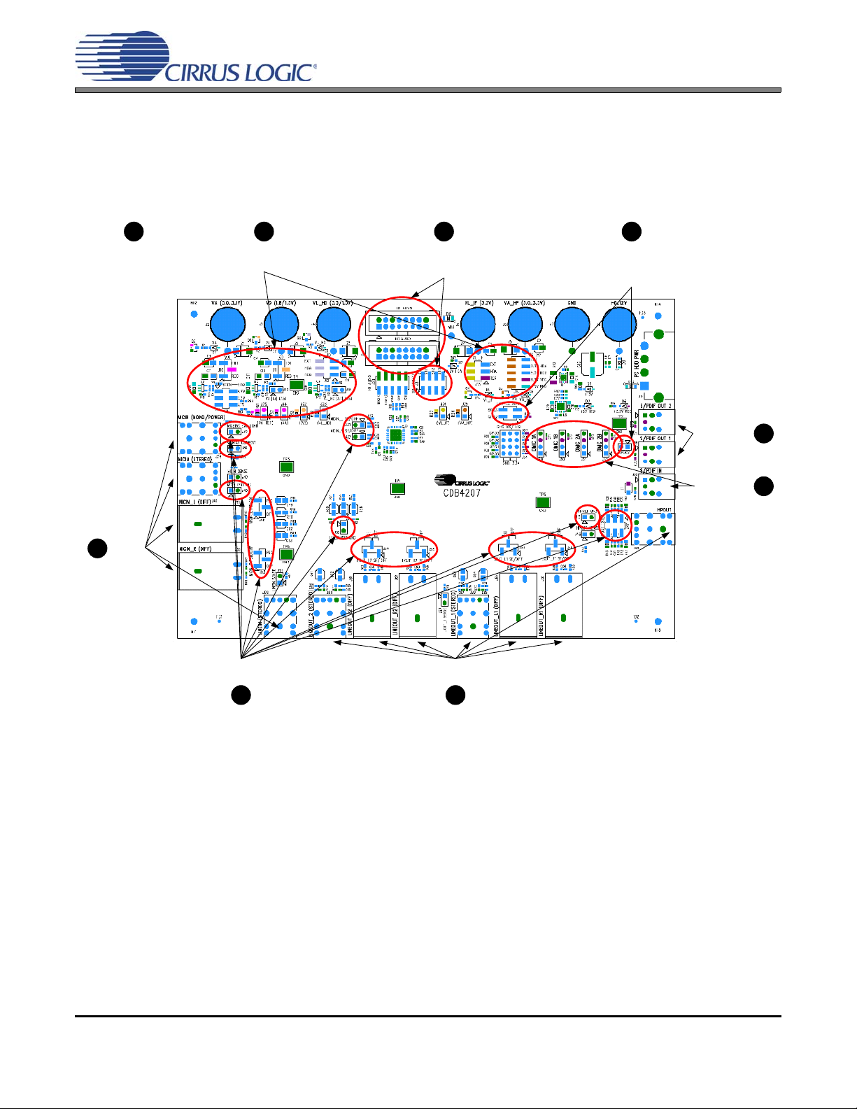
Figure 7. CDB4207 Component Map
16 DS880DB1
Page 17

CDB4207
Figure 8. CDB4207 Top Layer
DS880DB1 17
Page 18

CDB4207
Figure 9. CDB4207 Inner Layer 1 - Ground
18 DS880DB1
Page 19

CDB4207
Figure 10. CDB4207 Inner Layer 2 - Power
DS880DB1 19
Page 20

CDB4207
Figure 11. CDB4207 Bottom Layer
20 DS880DB1
Page 21

5. ORDERING INFORMATION
Product Description Included Hardware Order #
CDB4207
CS4207
Evaluation Board
1 x CDB4207
1 x 16-pin HD Audio cable
6. REVISION HISTORY
Release Date Changes
DB1 NOV 2009 Initial Release
CDB4207
CDB4207
DS880DB1 21
Page 22

CDB4207
Contacting Cirrus Logic Support
For all product questions and inquiries, contact a Cirrus Logic Sales Representative.
To find the one nearest you, go to www.cirrus.com
.
IMPORTANT NOTICE
Cirrus Logic, Inc. and its subsidiaries (“Cirrus”) believe that the information contained in this document is accurate and r eliable. However, the information is subject
to change without noti ce and is p rovided “AS IS” wit hout warran ty of any k ind (expr ess or i mplied). Customers are advis ed to ob tain the latest version of relevant
information to verify, before placing orders, that information being relied on is current and complete. All products are sold subject to the terms and conditions of sale
supplied at the time of order acknowledgment, including those pertaining to warranty, indemnification, and limitation of liability. No responsibility is assumed by Cirrus
for the use of this information, including use of this information as the basis for manufacture or sale of any items, or for infringement of patents or other rights of third
parties. This document is the property of Cirrus and by furnishing this information, Cirrus grants no license, express or implied under any patents, mask work rights,
copyrights, trademarks, trade secrets or other inte llectual property rig hts. Cirrus owns the copyrights associated with the information contained herein and gives consent for copies to be made of the information only for use within your organization with respect to Cirrus integrated circuits or other products of Cirrus. This consent
does not extend to other copying such as copying for general distribution, advertising or promotional purposes, or for creating any work for resale.
CERTAIN APPLICATIONS USING SEMICONDUCTOR PRODUCTS MAY INVOLVE POTENTIAL RISKS OF DEATH, PERSONAL INJURY, OR SEVERE PROPERTY OR ENVIRONMENTAL DAMAGE (“CRITICAL APPLICATIONS”). CIRRUS PRODUCTS ARE NOT DESIGNED, AUTHORIZED OR WARR ANTED FOR USE
IN PRODUCTS SURGICALLY IMPLANTED INTO THE BODY, AUTOMOTIVE SAFETY OR SECURITY DEVICES, LIFE SUPPORT PRODUCTS OR OTHER CRITICAL APPLICATIONS. INCLUSION OF CIRRUS PRODUCTS IN SUCH APPLICATIONS IS UNDERSTOOD TO BE FULLY AT THE CUSTOM ER’S RISK AND CIRRUS DISCLAIMS AND MAKES NO WARRANTY, EXPRESS, STATUTORY OR IMPLIED, INCLUDING THE IMPLIED WARRANTIES OF M ERCHANTABILITY AND
FITNESS FOR PARTICULAR PURPOSE, WITH REGARD TO ANY CIRRUS PRODUCT THAT IS USED IN SUCH A MANNER. IF THE CUSTOMER OR CUSTOMER’S CUSTOMER USES OR PERMITS THE USE OF CIRRUS PRODUCTS IN CRITICAL APPLICATIONS, CUSTOMER AGREES, BY SUCH USE, TO FULLY
INDEMNIFY CIRRUS, ITS OFFICERS, DIRECTORS, EMPLOYEES, DISTRIBUTORS AND OT HER AGE NTS FRO M ANY AND AL L LI ABI L IT Y, I NCL UDING ATTORNEYS’ FEES AND COSTS, THAT MAY RESULT FROM OR ARISE IN CONNECTION WITH THESE USES.
Cirrus Logic, Cirrus, and the Cirrus Logic logo design s ar e tra de m a rks of Ci rru s Lo gi c, Inc. All o ther bra nd and product names in this document may be trademarks
or service marks of their respective owners.
22 DS880DB1
 Loading...