

Page 1
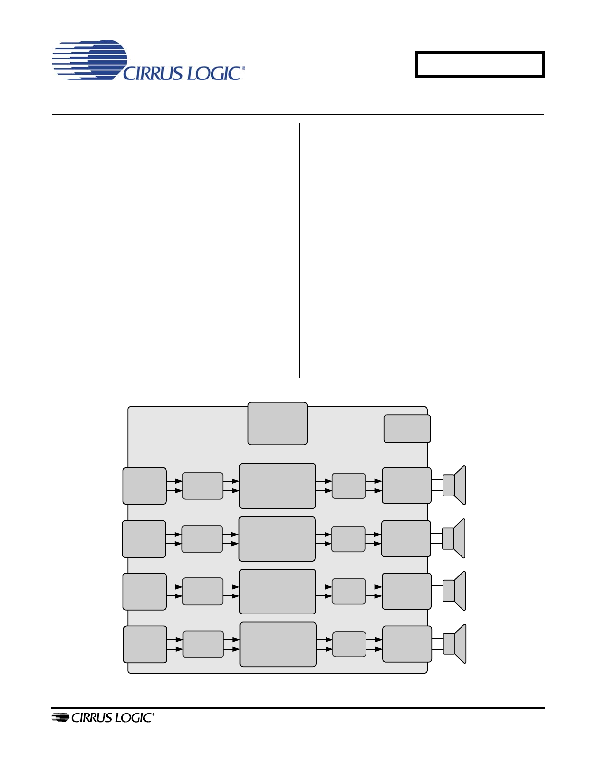
Control Switch
(S1)
Speaker
Output
(J11)
Optional
Gain
Adjustment
Analog
Input
(J10)
CS35L00
(U1)
Optional
Output
Filter
VBATT
Power (J1)
4 or 8
Speaker
Output
(J21)
Optional
Gain
Adjustment
Analog
Input
(J20)
CS35L00
(U2)
Optional
Output
Filter
4 or 8
Speaker
Output
(J31)
Optional
Gain
Adjustment
Analog
Input
(J30)
CS35L00
(U3)
Optional
Output
Filter
4 or 8
Speaker
Output
(J41)
Optional
Gain
Adjustment
Analog
Input
(J40)
CS35L00
(U4)
Optional
Output
Filter
4 or 8
CDB35L00-X4
2.7 W x 4 CS35L00 Amplifier Demonstration Board
Features
Contains 4 CS35L00 Hybrid Class-D Amplifiers
Selectable +6 dB or +12 dB Gain
Selectable Operational Modes
Device Shutdown Control
Delivers 2.7 W/Ch into 4 at 10 % THD+N
Delivers 1.6 W/Ch into 8 at 10 % THD+N
Differential Mono Analog Inputs for each
CS35L00 Amplifier
Demonstrates Recommended 4-Layer Layout
and Grounding Arrangements
– Optional Output Filter Connections
– Optional Gain Adjustment Resistors
Powered by Single +2.5-5.5 V Power Supply
Description
The CDB35L00-X4 demonstrates the CS35L00 high-efficiency Hybrid Class-D audio amplifier. This
demonstration board implements a four-channel, quad
amplifier system that delivers 2.7 W per full-bridge
channel into 4- loads using a single +5 V supply.
Differential audio inputs can easily be connected
through the J10, J20, J30, and J40 headers. If desired,
the gain can be adjusted through the optional input
resistors.
Component landings are available for an optional EMI
output filter.
The CDB35L00-X4 can be configured to evaluate the
four operational modes and two gain settings of the
CS35L00 amplifier. Mode, Gain, and Shutdown control
is available through the S1 switch. Hybrid control is
available through the R13, R23, R33, and R43 resistors.
ORDERING INFORMATION
CDB35L00 CS35L00-X4 Demo Board
http://www.cirrus.com
Copyright Cirrus Logic, Inc. 2010
(All Rights Reserved)
APR '10
DS913DB2
Page 2

TABLE OF CONTENTS
1. SYSTEM OVERVIEW ............................................................................................................................. 3
1.1 CS35L00 Hybrid Class-D Amplifier .................................................................................................. 3
1.2 Power Supply ................................................................................................................................... 3
1.3 Operational Modes ........................................................................................................................... 3
1.3.1 Operational Mode Control ....................................................................................................... 3
1.4 Shutdown Control ............................................................................................................................ 4
1.4.1 Shutdown Control Resistors .................................................................................................... 5
1.5 Gain Control ..................................................................................................................................... 5
1.5.1 Optional Gain Adjustment Resistors .......................................................................................5
1.6 Differential Analog Inputs ................................................................................................................. 6
1.7 Speaker Outputs .............................................................................................................................. 6
1.7.1 Optional Speaker Output EMI Filter Components ........... ........................................................ 6
2. GROUNDING AND POWER SUPPLY DECOUPLING .......................................................................... 7
2.1 Power Supply Decoupling ................................................................................................................ 7
2.2 Electromagnetic Interference (EMI) ................................................................................................. 7
2.2.1 Suppression of EMI at the Source ......................... ... .... ... ... ... ... ............................................... 7
3. SYSTEM CONNECTORS AND JUMPERS ....... ... ... ... .... .......................................... ... ... ........................ 8
4. CDB SCHEMATIC .................................................................................................................................. 9
4.1 Bill of Materials ............................................................................................................................... 10
5. CDB LAYOUT ....................................................................................................................................... 11
6. REVISION HISTORY ............................................................................................................................ 12
CDB35L00-X4
LIST OF FIGURES
Figure 1.Hybrid Control Resistors ............................................................................................................... 4
Figure 2.Shutdown Control Resistors .......................... ... .... ... ... ... .... ... ... ... ... .... ... ... ... .................................. 5
Figure 3.Optional Bypass Trace Cut Locations for U1 ................................................................................ 6
Figure 4.CDB35L00-X4 Schematic .... .... ... ... ... ... .... ... ... ... .... ... ... ... .... ... ... ... ... .... ... ... ... .... ... ........................... 9
Figure 5.CDB35L00-X4 Top Side Component Placement ........................................................................ 11
Figure 6.CDB35L00-X4 Bottom Side Component Placement ................................................................... 11
Figure 7.CDB35L00-X4 Layer 1 Copper ................................ ................................................................... 11
Figure 8.CDB35L00-X4 Layer 2 Copper ................................ ................................................................... 11
Figure 9.CDB35L00-X4 Layer 3 Copper ................................ ................................................................... 11
Figure 10.CDB35L00-X4 Layer 4 Copper ................................................................................................. 11
LIST OF TABLES
Table 1. S1 Switch GAIN & MODE Configurations ..................................................................................... 3
Table 2. Hybrid Control Resistor & S1 Switch MODE Configurations . ............. ............. ............ ............. ..... 4
Table 3. S1 Switch Default Shutdown Configurations ................................................................................. 5
Table 4. System Input and Output Connections ......................................................................................... 8
Table 5. S1 Switch Settings ........................................................................................................................ 8
Table 6. Bill of Materials Listing ................................................................................................................ 10
2 DS913DB2
Page 3
CDB35L00-X4
Table 1. S1 Switch GAIN & MODE
Configurations
1. SYSTEM OVERVIEW
The CDB35L00-X4 demonstration board is an practical means for evaluating the CS35L00 2.7 W Hybrid Class-D
amplifier with low idle current consumption. A differential mono analog input signal interface is provided for each
device. Optional input gain and output filtering component pl aceholders are provided for easy modification to custom
tune the CS35L00 for the user’s specific system requirements.
1.1 CS35L00 Hybrid Class-D Amplifier
The CS35L00 Hybrid Class-D amplifier is a 2.7 W mono, full-bridge, closed-loop, audio amplif ier availa ble
in a 10-pin, 3 mm x 3 mm, DFN package. A complete description of the CS35L00 is included in the CS35L00
product data sheet.
1.2 Power Supply
A single +2.5 to +5.5 VDC power supply is required to power the CDB35L00-X4. The supply must be capable of delivering sufficient current for the intended power output. The supply provides power to each of the
four CS35L00 amplifiers. The power supp ly connection to the board is provid ed by the header J1. The positive terminal is labeled VBATT. The ground terminal is labeled GND.
1.3 Operational Modes
The CS35L00 device has 4 different operational modes. Each of the 4 operational modes requires different
board configuration as described in Section 1.3.1 and Section 1.3.1.1. The operational modes of the
CS35L00 are listed below. More information on the specifics of each ope ra tiona l mod e can b e found in th e
CS35L00 product datasheet.
• SD: Standard Class-D Mode
• FSD: Reduced Frequency Standard Class-D Mode
• HD: Hybrid Class-D Mode
• FHD: Reduced Frequency Hybrid Class-D Mode
The CDB35L00-X4 demonstration board schematic is shown in Figure 4 on page 9.
1.3.1 Operational Mode Control
Using a combination of the S1 switch and the hybrid control resistors, as described in Section 1.3.1.1,
allows the CDB35L00-X4 to be configured in all 4 of the operational modes listed in Section 1.3.
Each CS35L00’s MODE pin on the CDB35L00-X4
board is connected to the S1 switch labeled MODE as
shown in Figure 4 on page 9. The MODE pin controls
whether all four of the CS35L00 devices on the
CDB35L00-X4 board are operating in one of the reduced frequency modes (FSD or FHD) or in one of the
higher frequency modes (SD or HD).
Table 1 on page 3 and Table 3 on page 5 show the S1 switch-controlled configuration options on the
CDB35L00-X4 board. More configuration options are available by removing or repopula ting 0 resistors
as described in Section 1.4.
LOW
HIGH
GAIN MODE
+12 dB FSD / FHD
+6 dB SD / HD
Note: In order to avoid transient audio signals, the CS 35L00 devices sh ould be shutdown either via the
S1 switch or by removing power when the operational mode is being changed.
DS913DB2 3
Page 4
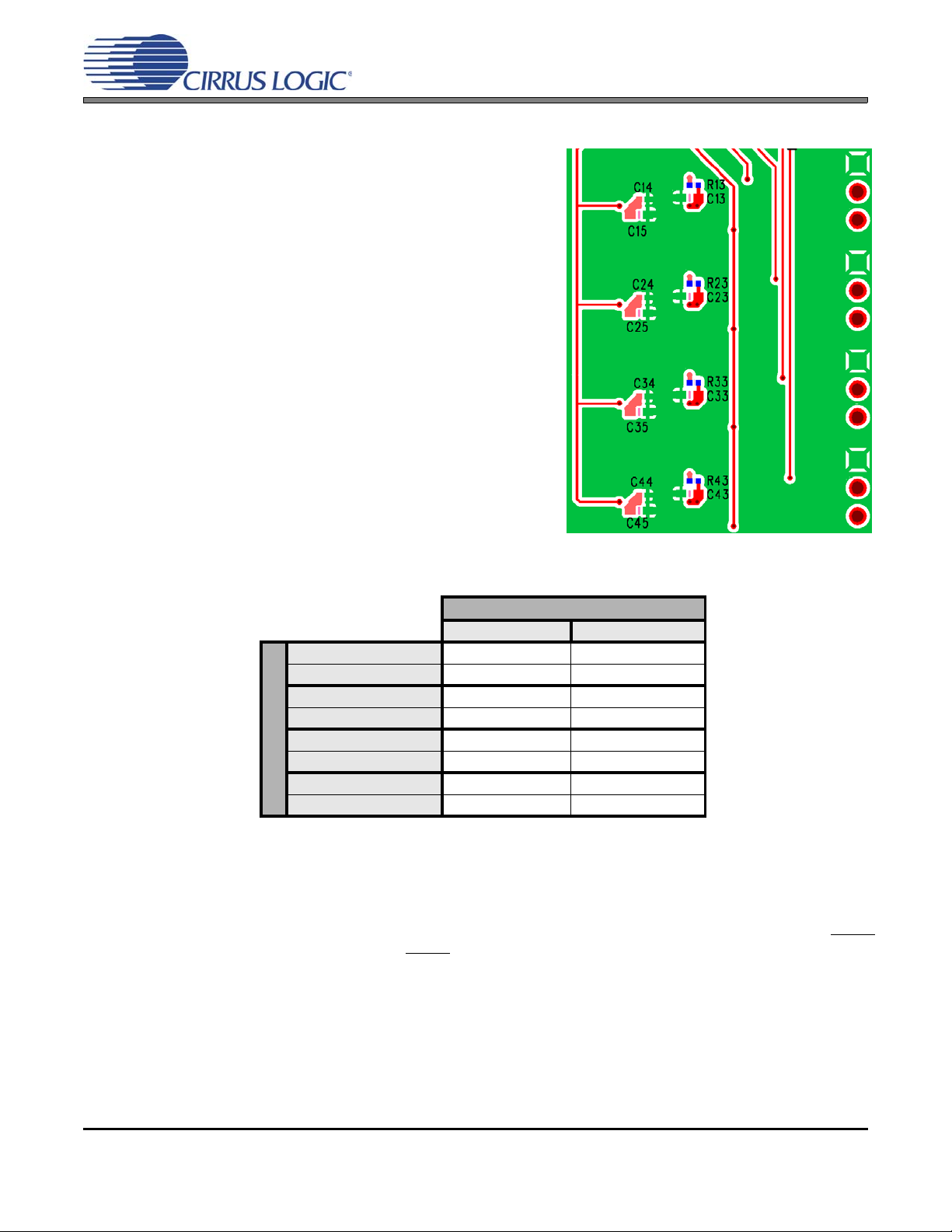
1.3.1.1 Hybrid Control Resistor Configuration
Figure 1. Hybrid Control Resistors
Each CS35L00 device has a hybrid control resistor. When
the hybrid control resistor for each CS35L00 is populated,
it connects the LFILT+ pin to VBATT and enables the
Standard Class-D functionality (SD or FSD modes) for the
corresponding device. When the hybrid control resistor
for each CS35L00 is not populated, LFILT+ is floating,
and the Hybrid Class-D functionality (HD or FHD modes)
is enabled.
The hybrid control resistors (R13, R23, R33, R43) are located on the bottom side of the board adjacent to the
LFILT+ decoupling capacitor and are highlighted in blue
in Figure 1.
A combination of the hybrid control resistors and the S1
MODE switch allow the CS35L00 devices (U1-U4) on the
CDB35L00-X4 board to be configured in all 4 of the op erational modes. There is no requirement to have the all
four of the CS35L00 devices configured in the same
mode. Each device can be configured to the user’s requirements. Table 2 lists the configuration options available using the hybrid control resistors and the S1 MODE
switch.
CDB35L00-X4
Hybrid Control Resistor
Table 2. Hybrid Control Resistor & S1 Switch MODE Configurations
1.4 Shutdown Control
The S1 switch implements shutdown control for the four CS35L00 devices on the CDB35L00-X4. SD1-2
controls the shutdown for U1 and U2. SD3-4 contro ls the shu tdown for U3 and U4 as shown in Table 3 and
on the schematic in Figure 4 on page 9.
S1 MODE Switch:
GND VBATT
R13: VBATT U1 = FSD U1 = SD
R13: Removed U1 = FHD U1 = HD
R23: VBATT U2 = FSD U2 = SD
R23: Removed U2 = FHD U2 = HD
R33: VBATT U3 = FSD U3 = SD
R33: Removed U3 = FHD U3 = HD
R43: VBATT U4 = FSD U4 = SD
R43: Removed U4 = FHD U4 = HD
4 DS913DB2
Page 5

1.4.1 Shutdown Control Resistors
Figure 2. Shutdown Control Resistors
The CDB35L00-X4 contains 0 ohm resistors (R1-R4) which
allow the individual CS35L00 shutdown pins to be disconnected from the S1 switch or connected to an external control device. These resistors are located on the back side of
the CDB35L00-X4 board near S1, as shown highlighted in
blue in Figure 2.
CDB35L00-X4
R1-R4 are connected to SD
ommended that the individual shutdown line pull-up resistors
for U1-U4 (R10, R20, R30, R40) be left populated to help
prevent the individual SD
on U1-U4, respectively. It is rec-
control lines from floating.
SD1-2 SD3-4
LOW
HIGH
Table 3. S1 Switch Default Shutdown Configurations
U1 & U2 OFF U3 & U4 OFF
U1 & U2 ON U3 & U4 ON
1.5 Gain Control
The amplifier gain of the CS35L00 can be configured to operate with either a +6 dB gain or a +12 dB gain
as shown in Table 1 on page 3. The amplifier gain is selectable through the GAIN setting on the S1 switch.
This is connected to the GAIN_SEL pins on the four CS35L00 devices as shown in Figure 4 on page 9.
Note: The CS35L00 devices should be placed into shutdow n via either the S1 switch or by removing pow-
er before changing the GAIN setting.
1.5.1 Optional Gain Adjustment Resistors
The CDB35L00-X4 contains optional gain adjustment resistor placeholders for each CS35L00 device
(R11, R12, R21, R22, R31, R32, R41, R42). By default these are not populated and the CS35L00 operates at its gain control setting as set by the S1 switch. See Table 1. The gain adjustment resistors are only
necessary when a gain of +6 dB or a gain of +12 dB is not desired. By adding series resistance to the
input, the signal amplitude to the CS35L00 will be reduced, and will reduce the overall system gain. The
typical input impedance values of the CS35L00 as well as how to calculate the resistor values for a desired gain can be found in the device datasheet.
In order to use the optional gain adjustment resistors for U1, the traces between the R11 pads and the
traces between the R12 pads must be cut in order to break the bypass circuit before populating R11 and
R12 with the desired resistance values. The location of these required cuts are shown in Figure 3 on page
6. After the trace between the pads has been broken, the gain adjustment resistors can be added to the
board.
The gain adjustment resistors for U2, U3, and U4 can be added in the same manner as is described for
U1 (above).
DS913DB2 5
Page 6

1.6 Differential Analog Inputs
Figure 3. Optional Bypass Trace Cut Locations for U1
Cut the bypass
traces before inserting the optional
input gain adjustment resistors
Cut the bypass
traces before
inserting the
optional output filter ferrite beads
The differential audio inputs into the four CS35L00 devices are provided by the 3-pin headers (J10, J20,
J30, and J40) through DC blocking capacitors (C11, C12, C21, C22, C31, C32, C41, C42). The DC blocking
capacitors allow for an analog source to connect directly to the CS35L00, regardless of any DC bias that
may be present between the analog audio source’s outputs and the CS35L00 inputs.
1.7 Speaker Outputs
The four CS35L00 power outputs pairs are each co nfigured for a single, full-bridg e, audio channel. The outputs are routed through an optional EMI output filter and then pr esented at the J11, J2 1, J31, and J41 headers. The CS35L00 is intended to be used with a 4 to 8 load.
1.7.1 Optional Speaker Output EMI Filter Components
The CDB35L00-X4 contains optional placeholders for a series ferrite bead (FB11, FB12, FB21, FB22,
FB31, FB32, FB41, FB42) and shunt capacitor (C16, C17, C26, C27, C36, C37, C46, C47) output filter.
For most applications with very short speaker leads between the CS35L00 and the spea ker, use of these
components will not be necessary. However, for systems with long signal paths between the CS35L00
and the speaker or if the system requires connecting to ca bles off the PCB, it is suggeste d that the ferrite
bead and capacitor are populated with the recommen ded values shown in Table 6 on page 10. These optional output filters will reduce EMI between the CS35L00 speaker outputs and the load.
CDB35L00-X4
In order to use the optional output filter ferrite beads for U1, the traces between the FB11 pads and the
traces between the FB12 pads must be cut to break the bypass circuit, before populating FB11 and FB12
with the desired component values. The location of these required cuts are shown in below in Figure 3.
The optional output filter ferrite beads for U2, U3, an d U4 can be added in the same manner as described
for U1 (above). The optional output filter capacitors can be populated with or without the addition of the
ferrite beads and require no board modifications.
6 DS913DB2
Page 7

CDB35L00-X4
2. GROUNDING AND POWER SUPPLY DECOUPLING
The CS35L00 requires careful attention to power supply and gr ounding arrang ements to op timize performance and
minimize radiated emissions. The device decoupling capacitors should be located as close to the CS35L00 as possible. This can be optimized by using both top and bottom side component population as demonstrated by the
CDB35L00-X4 board.
2.1 Power Supply Decoupling
Proper power supply decoupling is one key to maximizing the performa nce of a Class-D a mplifier. Figure 5
and Figure 6 on page 11 show the component placement for the CDB35L00-X4 board. Note the addition of
the C13, C23, C33, and C43 capacitors connected to the LFILT+ pin. This pin is used as decoupling for the
internal LDO regulator when operating in HD or FHD modes.
The small value decoupling cap acitors are pla ced as close a s possible to th e power pins of the CS35L00
on the CDB35L00-X4 board. It is recommended that the power supply decoupling capacitors reside on the
opposite side of the board from which the CS35L00 is populated on. This allows for very close placement
of the decoupling capacitors to the power supply pins of the CS35L00 without interfering with the diffe rential
audio inputs or differential audio outputs. This placement keeps the high-frequency current loop small to
minimize EMI.
2.2 Electromagnetic Interference (EMI)
This reference design is a board-level solution that is meant to control emissions by minimizing and suppressing them at the source, in contrast to containing them in an enclosure.
2.2.1 Suppression of EMI at the Source
Several techniques are used in the circuit design and board layout to minimize high-frequency fields in
the immediate vicinity of the high-power components. Specific techniques include the following:
• As mentioned in Section 2.1, effective power supply decoupling of high-frequency currents and mini-
mizing the loop area of the decoupling loop is one aspect of minimizing EMI.
• Differential input and output signals should be routed differentially whenever possible.
• A solid ground plane on the adjacent PCB layer underneath all high-frequency traces to minimize the
loop area of the return path.
• Optional output EMI filter component landings are available as described in Section 1.7.1, if emissions
need to be further reduced.
• Keeping the switching output filter components as close to the amplifier as possible.
DS913DB2 7
Page 8

3. SYSTEM CONNECTORS AND JUMPERS
CDB35L00-X4
Connector
Name
VBATT
GND
GND
IN1-
IN1+
OUT1-
OUT1+
GND
IN2-
IN2+
OUT2-
OUT2+
GND
IN3-
IN3+
OUT3-
OUT3+
GND
IN4-
IN4+
OUT4-
OUT4+
Reference
Designator
J1
J1
J10
J10
J10
J11
J11
J20
J20
J20
J21
J21
J30
J30
J30
J31
J31
J40
J40
J40
J41
J41
Pin Signal
Connector Function
Direction
1
2
1
2
3
1
2
1
2
3
1
2
1
2
3
1
2
1
2
3
1
2
Table 4. System Input and Output Connections
Input
Input
GND
Input
Input
Output
Output
GND
Input
Input
Output
Output
GND
Input
Input
Output
Output
GND
Input
Input
Output
Output
Positive connection from power supply, +2.5 to +5.5 VDC
GND connection from power supply.
GND reference connection
Differential analog input (-) to CS35L00, U1
Differential analog input (+) to CS35L00, U1.
Analog output (-) from CS35L00, U1
Analog output (+) from CS35L00, U1.
GND reference connection
Differential analog input (-) to CS35L00, U2
Differential analog input (+) to CS35L00, U2.
Analog output (-) from CS35L00, U2
Analog output (+) from CS35L00, U2.
GND reference connection
Differential analog input (-) to CS35L00, U3
Differential analog input (+) to CS35L00, U3.
Analog output (-) from CS35L00, U3
Analog output (+) from CS35L00, U3.
GND reference connection
Differential analog input (-) to CS35L00, U4
Differential analog input (+) to CS35L00, U4.
Analog output (-) from CS35L00, U4
Analog output (+) from CS35L00, U4.
S1 Control Name Function Function Selected
GAIN Gain U1-U4
MODE Mode U1-U4
SD1-2
SD3-4
Shutdown U1 & U2
Shutdown U3 & U4
Low = CS35L00 gain set to +12 dB
High = CS35L00 gain set to +6 dB
Low = CS35L00 frequency reduced operational mode (FSD or FHD)
High = CS35L00 non-frequency reduced operational mode (SD or HD)
Low = CS35L00 shutdown enabled
High = CS35L00 shutdown disabled
Low = CS35L00 shutdown enabled
High = CS35L00 shutdown disabled
Table 5. S1 Switch Settings
8 DS913DB2
Page 9

4. CDB SCHEMATIC
Figure 4. CDB35L00-X4 Schematic
CDB35L00-X4
DS913DB2 9
Page 10

CDB35L00-X4
4.1 Bill of Materials
The component listing below is shown for the CDB35L00-X4 board. Unpopulated (DNP) components ar e
listed with recommended components for reference purposes.
Qty Reference Designator(s) Description MFG / Part Number
1 C3 Capacitor, 1 F, X5R, 10V Kemet / C0603C105K8PAC
8 C11, C12, C21, C22, C31, C32,
C41, C42
4 C13, C23, C33, C43 Capacitor, 1F, X5R, 10V Kemet / C0603C105K8PAC
4 C15, C25, C35, C45 Capacitor, 10F, X5R, 6.3 V Kemet / C0603C106M9PAC
4 C14, C24, C34, C44 Capacitor, 0.1 F, X7R, 16V Kemet / C0402C104K4RAC
2 R5, R6 Resistor, 4.7 k
8 R1, R2, R3, R4, R13, R23, R33,
R43
4 R10, R20, R30, R40 Resistor, 47 k
4 U1, U2, U3, U4 Hybrid Class-D DFN Amp Cirrus Logic / CS35L00-CWZ
1 S1 Switch, 4 POS, DIP Grayhill / 76SB04T
(DNP) C16, C17, C26, C27, C36, C37,
C46, C47
(DNP) FB11, FB12, FB21, FB22, FB31,
FB32, FB41, FB42
(DNP) R11, R12, R21, R22, R31, R32,
R41, R42
Capacitor, 0.1 F, X7R, 16V Kemet / C0402C104K4RAC
, 1/10W Dale / CRCW06034K70JNEA
Resistor, 0 , 1/16W Yageo / RC0402JR-070RL
, 1/16W Dale / CRCW040247K0JNED
Capacitor, 1 nF, X7R, 50V Murata / GRM155R71H102KA01D
Ferrite Bead, 220
Resistor, 0 , 1/16W Yageo / RC0402JR-070RL
@ 100MHz TDK / MPZ1608S221A
Table 6. Bill of Materials Listing
10 DS913DB2
Page 11

5. CDB LAYOUT
Figure 5. CDB35L00-X4 Top Side
Component Placement
Figure 6. CDB35L00-X4 Bottom
Side Component Placement
Figure 7. CDB35L00-X4 Layer 1
Copper
Figure 8. CDB35L00-X4 Layer 2
Copper
Figure 9. CDB35L00-X4 Layer 3
Copper
Figure 10. CDB35L00-X4 Layer 4
Copper
CDB35L00-X4
DS913DB2 11
Page 12

6. REVISION HISTORY
Contacting Cirrus Logic Support
For all product questions and inquiries, contact a Cirrus Logic Sales Representative.
To find the one nearest to you, go to www.cirrus.com.
IMPORTANT NOTICE
Cirrus Logic, Inc. and its subsidiaries (“Ci rrus”) believe that the information containe d in this document is accurate and reliable. However, the information is subject
to change without noti ce and is p rovided “AS IS” wit hout warran ty of any k ind (expr ess or i mplied). Customers are advis ed to ob tain the latest version of relevant
information to verify, before placing orders, that information being relied on is current and complete. All products are sold subject to the terms and conditions of sale
supplied at the time of order acknowledgment, including those pertaining to warranty, indemnification, and limitation of liability. No responsibility is assumed by Cirrus
for the use of this information, including use of this information as the basis for manufacture or sale of any items, or for infringement of patents or other rights of third
parties. This document is the property of Cirrus and by furnishing this information, Cirrus grants no license, express or implied under any patents, mask work rights,
copyrights, trademarks, trade secrets or other inte llectual property rig hts. Cirrus owns the copyrights associated with the information contained herein and gives consent for copies to be made of the information only for use within your organization with respect to Cirrus integrated circuits or other products of Cirrus. This consent
does not extend to other copying such as copying for general distribution, advertising or promotional purposes, or for creating any work for resale.
CERTAIN APPLICATIONS USING SEMICONDUCTOR PRODUCTS MAY INVOLVE POTENTIAL RISKS OF DEATH, PERSONAL INJURY, OR SEVERE PROPERTY OR ENVIRONMENTAL DAMAGE (“CRITICAL APPLICATIONS”). CIRRUS PRODUCTS ARE NOT DESIGNED, AUTHORIZED OR WARR ANTED FOR USE
IN PRODUCTS SURGICALLY IMPLANTED INTO THE BODY, AUTOMOTIVE SAFETY OR SECURITY DEVICES, LIFE SUPPORT PRODUCTS OR OTHER CRITICAL APPLICATIONS. INCLUSION OF CIRRUS PRODUCTS IN SUCH APPLICATIONS IS UNDERSTOOD TO BE FULLY AT THE CUSTOM ER’S RISK AND CIRRUS DISCLAIMS AND MAKES NO WARRANTY, EXPRESS, STATUTORY OR IMPLIED, INCLUDING THE IMPLIED WARRANTIES OF MER CHANTABILITY AND
FITNESS FOR PARTICULAR PURPOSE, WITH REGARD TO ANY CIRRUS PRODUCT THAT IS USED IN SUCH A MANNER. IF THE CUSTOMER OR CUSTOMER’S CUSTOMER USES OR PERMITS THE USE OF CIRRUS PRODUCTS IN CRITICAL APPLICATIONS, CUSTOMER AGREES, BY SUCH USE, TO FULLY
INDEMNIFY CIRRUS, ITS OFFICERS, DIRECTORS, EMPLOYEES, DISTRIBUTORS AND OT HER AGE NTS FRO M ANY AND AL L LI ABI L IT Y, I NCL UDING ATTORNEYS’ FEES AND COSTS, THAT MAY RESULT FROM OR ARISE IN CONNECTION WITH THESE USES.
Cirrus Logic, Cirrus, and the Cirrus Logic logo design s ar e tra de m a rks of Ci rru s Lo gi c, Inc. All o ther bra nd and product names in this document may be trademarks
or service marks of their respective owners.
Release Changes
DB1 – Initial Release
DB2 – Updated 10% output power numbers on the front page to match DS906A2 device datasheet.
– Updated Figure 4 on page 9 to match the updated CDB35L00-X4 Rev A1 schematic.
– Updated BOM values for C6 & C7 in Table 6 on page 10 to match the udpated Rev A1 schematics and
the typical connection diagram in the DS906A2 device datasheet. All CDB35L00-X4 boards with an
assembly date of 02/15/10 or earlier contain components from the Rev A0 BOM.
CDB35L00-X4
12 DS913DB2
 Loading...