

Page 1
Evaluation Board for CS3308
CDB3308
Features
Single-ended Analog Inputs
Single-ended Analog Outputs
Supports AC and DC-Coupled Analog I/O
Flexible Serial Control I/O Headers
– Serial Control Input Header to
Accommodate On-board and External
Serial Controllers
– Serial Control Output Headers for
“Chaining” Serial Control Across Multiple
CDB3308 Evaluation Boards
– 3.3 V Logic Interface Level
Demonstrates Recommended Layout and
Grounding Arrangements
Minimal Power Supply Requirements
– ±5 V and Ground
Windows
– Easy and Intuitive Graphical Interface to
– Supports USB and RS-232 PC
®
Compatible Software Interface
Channel and Master Volume Controls
Connectivity
Description
The CDB3308 evaluation board is an excellent means
for evaluating the CS3308 analog volume control. Evaluation requires an analog signal source and analyzer,
power supplies, and a Windows PC compatible
computer.
Standard RCA phono jacks are provided to easily interface external analog signals with the evaluation board.
Each of the CS3308’s inputs and outputs may be independently AC or DC-coupled to their respective I/O
connectors.
The Windows software provides a GUI to make configuration of the CDB3308 easy. The software
communicates through the PC’s USB or Serial port to
configure the control port registers so that all features of
the CS3308 can be evaluated.
As an alternative to the serial control provided via a PC,
the evaluation board may be configured to accept external control signals for operation in a user application
during system development.
To facilitate multi-CS3308 system design efforts, headers are provided for connecting serial control signals
between multiple CDB3308 evaluation boards.
ORDERING INFORMATION
CDB3308 Evaluation Board
8-Channel
Passive
Inputs
USB/RS232
PC Interface
http://www.cirrus.com
AC/DC
Coupling
CS3308
8-Channel
Digitally Controlled
Analog Volume Control
PC or External
Serial Control Input
Copyright © Cirrus Logic, Inc. 2006
(All Rights Reserved)
AC/DC
Coupling
External
Serial Control Output
8-Channel
Passive
Outputs
MAY '06
DS702DB2
Page 2

TABLE OF CONTENTS
1. SYSTEM OVERVIEW ............................................................................................................................. 3
1.1 Power ............................................................................................................................................... 3
1.2 Grounding and Power Supply Decoupling ...................... ... .... ... ... ... ... .... ........................................... 3
1.3 CS3308 Analog Volume Control ..................... ... ... .... ... ... ... .... ... ... ... ... .... ... ........................................ 3
1.4 External Control Headers ................................................................................................................. 3
1.5 Analog Inputs .................................................................................................................................... 4
1.6 Analog Outputs ................................................................................................................................. 4
1.7 PC Interfaces .................................................................................................................................... 4
2. PC SOFTWARE CONTROL ................................................................................................................... 5
2.1 CS3308 Controls Tab ....................................................................................................................... 5
2.2 Register Maps Tab ........................................................................................................................... 6
3. PERFORMANCE PLOTS ....................................................................................................................... 7
4. SYSTEM CONNECTIONS & JUMPERS ................................................................................................8
5. CDB BLOCK DIAGRAM ........................................................................................................................ 9
6. CDB SCHEMATICS .............................................................................................................................. 10
7. CDB LAYOUT ....................................................................................................................................... 13
8. REVISION HISTORY ............................................................................................................................ 16
LIST OF FIGURES
Figure 1.CS3308 Controls Tab .................................................................... .... ... ... ..................................... 5
Figure 2.Register Maps Tab ............................ ... .... ... ... ... .... ... ... ... .... ... ... ... ... .... ........................................... 6
Figure 3.Frequency Response .................................................................................................................... 7
Figure 4.THD+N vs. Amplitude .................................... ... .... ... ... ... .... ... ... ... .................................................. 7
Figure 5.THD+N vs. Frequency ...................................... .... ... ..................................................................... 7
Figure 6.Crosstalk .............................................. .... ... ... ....................................... ... ... .... .............................. 7
Figure 7.Block Diagram ............................. ... ... ... .... ... ... ... .......................................... .... ... ........................... 9
Figure 8.CS3308 ... ... .... ... ... ... .... ... ................................................................................. ............................ 10
Figure 9.Analog Inputs and Outputs ...................................................................... ... .... ... ... ...................... 11
Figure 10.Serial Control / Power ............................................................................................................... 12
Figure 11.Silkscreen Top ....................... ... ... ... ... .... ... ... ... .... .......................................... ... ... ...................... 13
Figure 12.Top Side Copper Layer ... ... .... ... ... ............................................................................................. 14
Figure 13.Bottom Side Copper Layer ........................................................................................................ 15
CDB3308
LIST OF TABLES
Table 1. System Connections ..................................................................................................................... 8
Table 2. On-Board Switches ....................................................................................................................... 8
Table 3. System Headers ............................................................................................................................ 8
2 DS702DB2
Page 3

CDB3308
1. SYSTEM OVERVIEW
The CDB4265 evaluation board is an excellent means for evaluating the CS3308 digitally controlled analog volume
control. Analog audio signal interfac es are pro vided, an on-board microcontroller and USB/RS-232 PC interface is
used for easily configuring the CS3308’s internal registers, and a USB cable is included for use with the FlexGUI
Windows configuration software.
The CDB3308 schematic set is shown in Figure 8 through Figure 10.
1.1 Power
Power (±5 V) must be supplied to the evaluation board through the red VA+ and green VA- binding posts.
An on-board regulator provides a 3.3 V supply to the digital circuitry. All voltage inputs must be re fe re n ced
to the single black binding post ground connector (see the System Connections table on page 8).
WARNING: Please refer to the CS3308 data sheet for allowable voltage levels.
1.2 Grounding and Power Supply Decoupling
The CS3308 requires careful attention to power supply and grounding arrangements to optimize performance. Figure 7 on page 9 provides an overview of the connections to the CS3308. Figure 11 on page 13
shows the component placement. Figure 12 on page 14 shows the top layout. Figure 13 on page 15 shows
the bottom layout. The decoupling capacitors are located as close to the CS3308 as possible. Extensive
use of ground plane fill in the evaluation board yields large reductions in radiated noise.
1.3 CS3308 Analog Volume Control
A complete description of the CS3308 is included in the CS3308 product data sheet.
The required configuration settings of the CS3308 are achieved via its control port registers, accessible
through the CS3308 tab of the Cirrus Logic FlexGUI software. A reg ister-level configuration interface is p rovided on the Register Maps tab. See the “PC Software Control” section on page 5 for more information.
1.4 External Control Headers
The evaluation board has been designed to allow interfacing with external systems via the headers J17,
J88, and J89.
The 15-pin, 3 column header, J17, provides bidirectional access to the CS3308’s SPI
digital control signals. The pins located in the column labeled “PC” connect to the on-board PC interface
circuitry, and those in the co lumn labeled “In” co nnect directly to t he CS3308’s digital co ntrol I/O pins. By
default, shunts are populated across these rows, connecting the PC interface to the CS3308’s digital control
I/O. To use an external digital control source, simply remove the shunts and connect a ribbon cable to the
“In” position. A single “GND” column for the ribbon cable’s ground connection is provided to mainta in signal
integrity. Two unpopulated pu ll-up resisto rs are a lso available should the CDB3308 be required to provide
the pull-up function for the I²C bus.
The 10-pin, 2 column header, J89, provides bidirectional access to the CS3308’s I²C SDA and SCL signals,
as well as unidirectional output access to the CS3308’s AD0, ENOut, and MUTE
signals are connected directly to their corresponding pi ns on the CS3308, as well as those on J17 described
above. The AD0, ENOut, and MUTE
their respective I/O pins on the CS3308. This header may be used to connect the serial control signals between 2 or more CDB3308’s (out of J89 on one and in to J17 on another) for multiple CS3308 I²C serial
control evaluation.
signals are re-driven versions of these signals as present directly on
TM
/I²C® and MUTE
signals. The SDA and SCL
DS702DB2 3
Page 4

The 10-pin, 2 column header, J88, provides unidirectional output access to the CS3308’s SPI MOSI and
CCLK signals, as well as its AD0, ENOut, and MUTE
present directly on their respective I/O pins on the CS3308. This header may be used to co nne ct the serial
control signals between 2 or m ore CDB3308’s (out of J88 on one an d in to J17 on another) for multiple
CS3308 SPI serial control evaluation.
1.5 Analog Inputs
RCA connectors supply the CS3308 analog inputs through single-ended passive circuits wi th no input filtering. Refer to the CS3308 data sheet for the maximum input signal level.
Each analog input may be AC or DC coupled to its respective RCA connector. This selection is made via
the 2-pin headers labeled “DC Couple Input” and placed adjacent to each input connector on the board. To
DC couple an input connector, place a shunt across the respective heade r. To AC couple an in put connector, remove the shunt from the respective header. By default, the input connectors are AC coupled to the
CS3308’s inputs.
1.6 Analog Outputs
The CS3308 analog outputs are routed through single-ended passive circuits with no output filtering and
connected to RCA jacks for easy evaluation.
Each analog output may be AC or DC coupled to its respective RCA connector. This selection is made via
the 2-pin headers labeled “DC Couple Output” and pla ced adjacent to each output connector on the board.
To DC couple an output connector, place a shunt across the respective header. To AC couple an output
connector, remove the shunt from the resp ective head er. By default, the output connectors are AC coupled
to the CS3308’s outputs.
CDB3308
signals. All of the signals re-driven versions of those
1.7 PC Interfaces
USB and RS-232 connections are provided to facilitate software control of the CS3308’s internal registers.
A graphical user interface is available for the CDB3308 to allow easy manip ulation of the CS3308’s internal
registers. See the CS3308 datasheet for complete internal register descriptions.
To enable the CDB3308, simply connect the supplied USB cable from an available USB port on a PC to the
USB connector (J37), or alternatively connec t a 9-pin serial cable from an available COM port on a PC to
the RS-232 connector (J42) and launch the Cirrus Logic FlexGUI software.
Refer to “PC Software Control” on page 5 for a description of the Graphical User Interface (GUI).
4 DS702DB2
Page 5
CDB3308
2. PC SOFTWARE CONTROL
The CDB3308 is designed for use with the Microsoft Windows based FlexGUI graphical user interface. This interface provides comprehensive control over the CS3308’s internal registers via a PC’s USB or RS-232 port.
The FlexGUI software may be downloaded and installed from www.cirrus.com/msasoftware.
Step-by-step instructions for using the FlexGUI are provided as follows:
1. Download and install the FlexGUI software from www.cirrus.com/msasoftware.
2. Connect the CDB3308 to a host PC using the supplied USB cable or a 9-pin serial cable.
3. Apply positive power, negative power, and ground to the VA+, VA-, and GND binding posts respectively.
4. Launch the FlexGUI software. The GUI will load and be displayed.
5. Un-check the “Power Down CS3308” check box to allow audio to pass th ro ug h th e de vice.
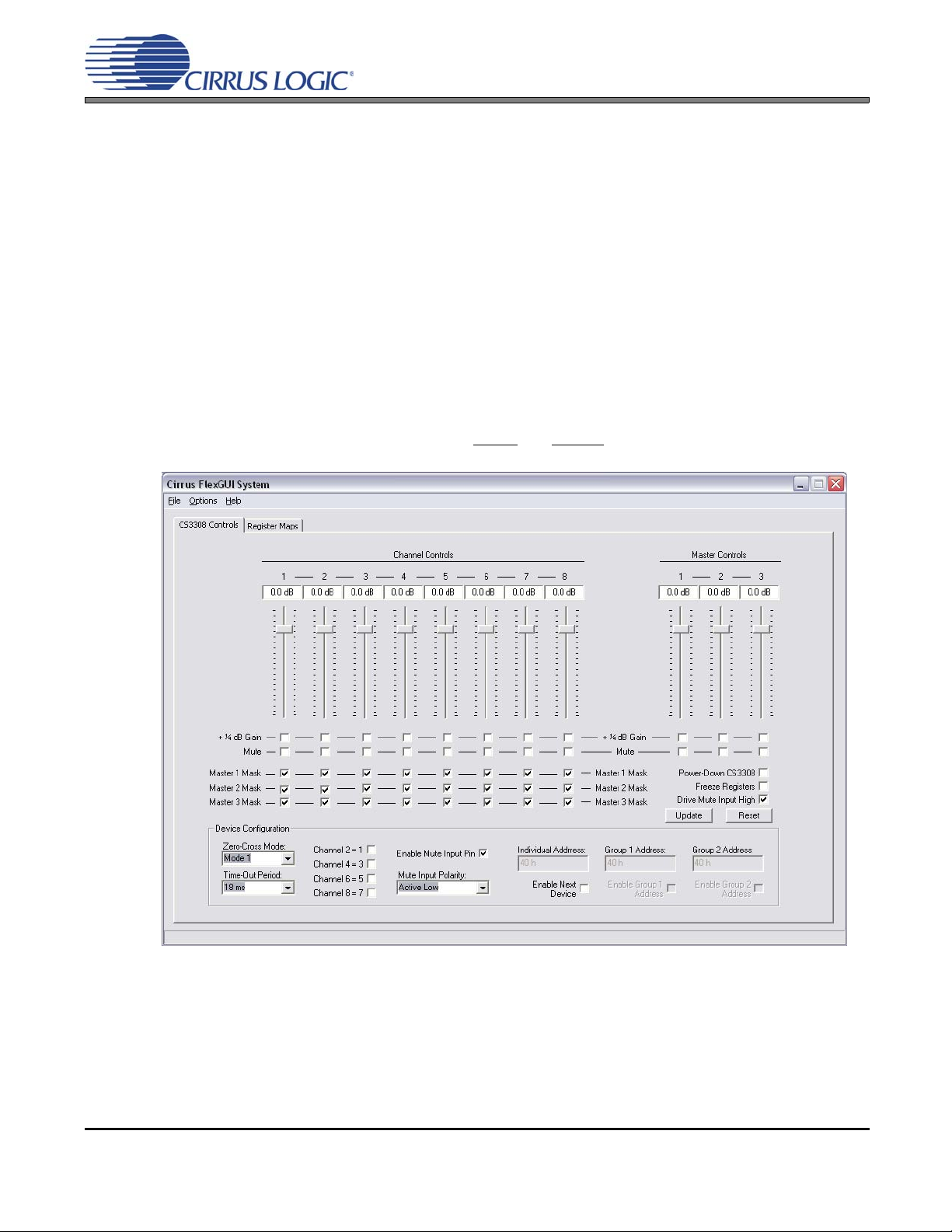
2.1 CS3308 Controls Tab
The CS3308 Controls tab provides a high-level intuitive interface to many of the configuration options of the
CS3308. Control over the state of the CS3308’s MUTE
and RESET input pins is also provided.
Figure 1. CS3308 Controls Tab
The Master X Mask check boxes are used to map each channel to the master controls. These check-boxes
reflect the state of their associated Master X Mask bits; when checked, the channel is un-masked.
The sliders facilitate control over the Ch X Volume registers, providing gain and attenuation in ½ dB steps.
The +¼ dB Gain check boxes are used to add an additional ¼ dB of gain to the volume level displayed for
each channel.
See the CS3308 datasheet for complete internal register descriptions.
DS702DB2 5
Page 6

2.2 Register Maps Tab
The Register Maps tab provides an easy register-level interface to the on-board devices. Register values
can be modified on a bit-wise or byte-wise basis. To modify a single bit, first select the register by clicking
its position in the register matrix, then click the appropriate push-button for the desired bit. To modify an
entire register, simply enter the register’s new value directly into the register matrix.
Within the Register Maps tab, the CS3308 tab is used to access the CS3308’s internal registers, and the
GPIO tab is used to access the on-board microcontroller outputs used to control the CS3308’s MUTE
and default I²C address.
CDB3308
input
Figure 2. Register Maps Tab
The Comm Mode Select box may be used to change the CS3308 ’s serial communication protocol between
I²C and SPI. The CS3308 will be automatically reset when the communication protocol is changed.
The software is only capable of addressing the CS3308 at its default address. If the CS3308’s individual
address is changed, the software will loose communication with the device until it is reset, thereby returning
to its default address. See the CS3308 datasheet for more information about the device’s individual address.
6 DS702DB2
Page 7

3. PERFORMANCE PLOTS
CDB3308
(TA= +25 ºC, VA+ = +5 V, VA- = -5 V, VD = +3.3 V, RL=100kΩ, CL=20pF, VIN=2V
Gain = 0 dB, Measurement Bandwidth = 20 Hz to 20 kHz, unless otherwise noted.)
+1
+0.9
+0.8
+0.7
+0.6
+0.5
+0.4
+0.3
+0.2
+0.1
d
B
r
+0
A
-0.1
-0.2
-0.3
-0.4
-0.5
-0.6
-0.7
-0.8
-0.9
-1
20 200k50 100 200 500 1k 2k 5k 10k 20k 50k 100k
Hz
Figure 3. Frequency Response Figure 4. THD+N vs. Amplitude
1
0.5
0.2
0.1
0.05
0.02
%
0.01
0.005
0.002
0.001
0.0005
0.0002
0.0001
20 20k50 100 200 500 1k 2k 5k 10k
Hz
Figure 5. THD+N vs. Frequency Figure 6. Crosstalk
1
0.5
0.2
0.1
0.05
0.02
%
0.01
0.005
0.002
0.001
0.0005
0.0002
0.0001
100m 3200m 300m 400m 500m 600m 700m 800m 900m 1 2
+0
-10
-20
-30
-40
-50
-60
-70
-80
d
B
r
-90
A
-100
-110
-120
-130
-140
-150
-160
-170
-180
20 20k50 100 200 500 1k 2k 5k 10k
Vrms
Hz
, FIN=1kHz,
RMS
DS702DB2 7
Page 8

4. SYSTEM CONNECTIONS & JUMPERS
CDB3308
Connector
Name
GND J5 Input Ground reference.
V A+ J8 Input Positive analog power. +5 V.
VA- J7 Input Negative analog power. -5 V.
In 1
In 2
In 3
In 4
In 5
In 6
In 7
In 8
Out 1
Out 2
Out 3
Out 4
Out 5
Out 6
Out 7
Out 8
USB I/O J37 Input/Output USB connection to PC for software control.
RS-232 I/O J42 Input/Output Serial RS-232 connection to PC for software control.
I²C/SPI Input J17 Input/Output Connection for internal/external I²C/SPI control signals.
I²C Output J89 Output Output connection for on-board I²C control signals.
SPI Output J88 Output Output connection for on-board SPI control signals.
C2 J36 Input/Output Connection for programming the on-board microcontroller (U46).
Reference
Designator
J29
J27
J11
J15
J55
J57
J71
J73
J19
J21
J46
J48
J62
J64
J79
J81
Signal
Direction Connector Function
Input Analog input to CS3308.
Output
Analog output from CS3308
Table 1. System Connections
.
Switch Name Reference Designator Switch Function
uC Reset J5 Resets the on-board microcontroller (U46).
Table 2. On-Board Switches
Reference
Connector Name
DC Couple Input 1
DC Couple Input 2
DC Couple Input 3
DC Couple Input 4
DC Couple Input 5
DC Couple Input 6
DC Couple Input 7
DC Couple Input 8
DC Couple Output 1
DC Couple Output 2
DC Couple Output 3
DC Couple Output 4
DC Couple Output 5
DC Couple Output 6
DC Couple Output 7
DC Couple Output 8
Designator Header Function
J2
J3
J16
J18
J58
J59
J74
J75
J32
J33
J51
J52
J67
J68
J84
J85
When a shunt is present across its pins, each header DC couples its respective input connector to the associated input of the CS3308
When no shunt is present across the header’s pins, its respective input connector will be AC coupled to the associated input of the CS3308
When a shunt is present across its pins, each header DC couples its respective output connector to the associated output of the CS3308
When no shunt is present across the header’s pins, its respective output
connector will be AC coupled to the associated output of the CS3308
Table 3. System Headers
.
.
.
.
8 DS702DB2
Page 9

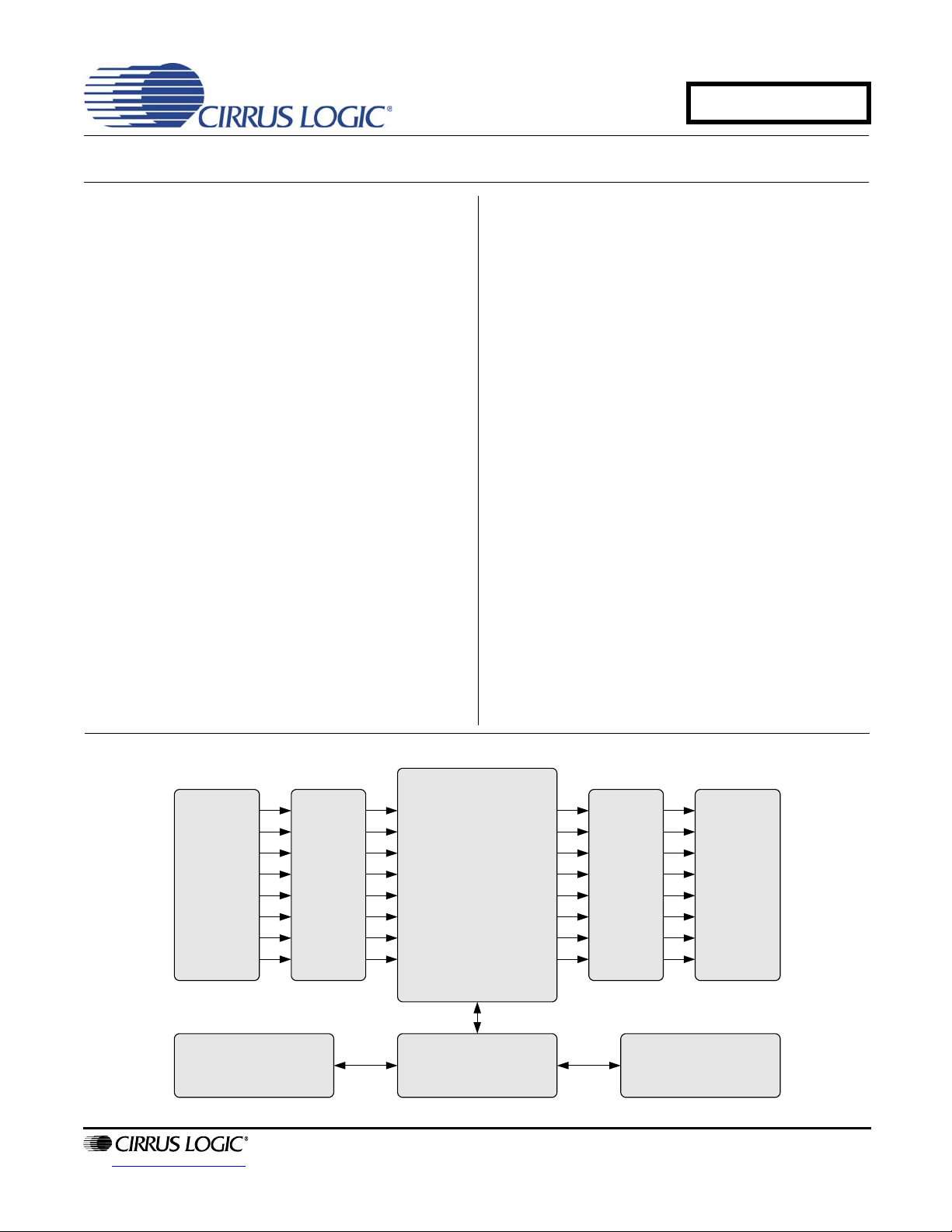
5. CDB BLOCK DIAGRAM
Passive
8-Channel
AC/DC
Coupling
CDB3308
Outputs
External
Serial Control Output
CS3308
8-Channel
AC/DC
Passive
8-Channel
Digitally Controlled
Analog Volume Control
Coupling
Inputs
PC or External
Serial Control Input
USB/RS232
PC Interface
Figure 7. Block Diagram
DS702DB2 9
Page 10

6. CDB SCHEMATICS
CDB3308
Figure 8. CS3308
Schematic Page 1
10 DS702DB2
Page 11

CDB3308
Figure 9. Analog Inputs and Outputs
Schematic Page 2
DS702DB2 11
Page 12

CDB3308
Figure 10. Serial Control / Power
Schematic Page 3
12 DS702DB2
Page 13

7. CDB LAYOUT
±5V
CDB3308
CDB3308
DS702DB2 13
Figure 11. Silkscreen Top
Page 14

CDB3308
Figure 12. Top Side Copper Layer
14 DS702DB2
Page 15

CDB3308
Figure 13. Bottom Side Copper Layer
DS702DB2 15
Page 16

8. REVISION HISTORY
Release Changes
DB1 Initial Release
DB2 Updated performance plots shown in Figures 3 - 6 on page 7.
CDB3308
Contacting Cirrus Logic Support
For all product questions and inquiries, contact a Cirrus Logic Sales Representative.
To find the one nearest to you, go to www.cirrus.com.
IMPORTANT NOTICE
Cirrus Logic, Inc. and its subsidiaries ("Cirrus") believe that the information contained in this document is accurate and reliable. However, the information is subject
to change without not ice and is pr ovided "AS IS" witho ut warr anty of any kind (express or implied). Customers are advised to obtain the latest version of relevant
information to verify, before placing orders, that information being relied on is current and complete. All products are sold subject to the terms and conditions of sale
supplied at the time of order acknowledgment, including those pertaining to warranty, indemnification, and limitation of liability. No responsibility is assumed by Cirrus
for the use of this information, including use of this information as the basis for manufacture or sale of any items, or for infringement of patents or other rights of third
parties. This document is the property of Cirrus and by furnishing this information, Cirrus grants no license, express or implied under any patents, mask work rights,
copyrights, trademarks, trade secrets or other inte llectual property rig hts. Cirrus owns the copyrights associated with the information contained herein and gives consent for copies to be made of the information only for use within your organization with respect to Cirrus integrated circuits or other products of Cirrus. This consent
does not extend to other copying such as copying for general distribution, advertising or promotional purposes, or for creating any work for resale.
CERTAIN APPLICATIONS USING SEMICONDUCTOR PRODUCTS MAY INVOLVE POTENTIAL RISKS OF DEATH, PERSONAL INJURY, OR SEVERE PROPERTY OR ENVIRONMENTAL DAMAGE (“CRITICAL APPLICATIONS”). CIRRUS PRODUCTS ARE NOT DESIGNED, AUTHORIZED OR WARRANTED FOR USE
IN AIRCRAFT SYSTEMS, MILITARY APPLICATIONS, PRODUCTS SURGICALLY IMPLANTED INTO THE BODY, AUTOMOTIVE SAFETY OR SECURITY DEVICES, LIFE SUPPORT PRODUCTS OR OTHER CRITICAL APPLICATIONS. INCLUSION OF CIRRUS PRODUCTS IN SUCH APPLICATIONS IS UNDERSTOOD TO BE FULLY AT THE CUSTOMER’S RISK AND CIRRUS DISCLAIMS AND MAKES NO WARRANTY, EXPRESS, STATUTORY OR IMPLIED,
INCLUDING THE IMPLIED WARRANTIES OF MERCHANTABILITY AND FITNESS FOR PARTICULAR PURPOSE, WITH REGARD TO ANY CIRRUS PRODUCT
THAT IS USED IN SUCH A MANNER. IF THE CUSTOMER OR CUSTOMER’S CUSTOMER USES OR PERMITS THE USE OF CIRRUS PRODUCTS IN CRITICAL
APPLICATIONS, CUSTOMER AGREES, BY SUCH USE, T O FULLY INDEMNIF Y CIRRUS, ITS OF FICE RS, DI RECTORS, EMPLOYEES, DISTRI BUTORS AND
OTHER AGENTS FROM ANY AND ALL LIABILITY, INCLUDING ATTORNEYS’ FEES AND COSTS, THAT MA Y RESULT FROM OR ARISE IN CONNECTION
WITH THESE USES.
Cirrus Logic, Cirrus, and the Cirrus Logic logo designs are trademarks of Cirrus Logic, Inc. All other brand and product names in this document may be trademarks
or service marks of their respective owners.
SPI is a trademark of Motorola, Inc.
I²C is a registered trademark of Philips Semiconductor.
Windows is a registered trademark of Microsoft Corporation.
16 DS702DB2
 Loading...