

Page 1
Application Note
Interfacing the CS5525/6/9 to the 68HC05
By Keith Coffey
AN89
INTRODUCTION
This applica tion note details the interfac e of Crys-
tal Semiconductor’s CS5525/6/9 Analog-to-Digital Converter (ADC) to a Motorola 68HC05
microcontroller. This note takes the reader through
a simple e xamp le de scribi ng how to co mmun icate
with the ADC. Al l algor ithms di scussed are included in the Appendix at the end of this note.
ADC DIGITAL INTERFACE
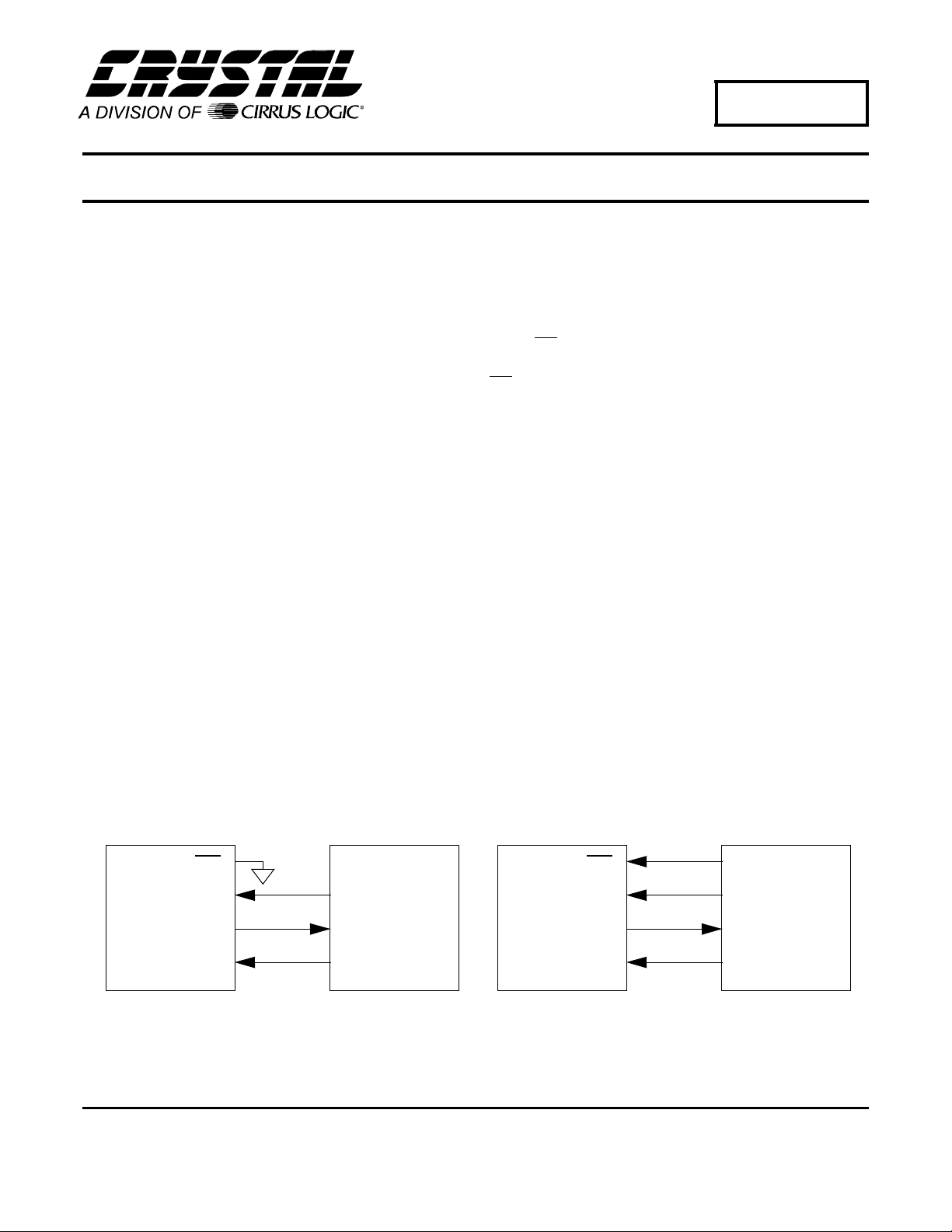
The CS5525/6/9 interface s to the 68HC05 t hrough
either a thre e-wir e or a four-wir e inte rface. Figure
1 depicts the interface between the two devices.
Though this software was written to interface to the
TM
SPI
modified to w ork in the four-wire format.
on the 68HC05, the algorithms can be easily
The ADC’s serial port consists of four control
lines: CS
CS
, SCLK, SDI, and SDO.
, Chip S elect, is the contro l line w hich e nables
access to the serial port.
SCLK, Serial Clock, is the bit-clock which controls
the shifting of data to or from the ADC’s serial
port.
SDI, Serial Data In, is the data signal used to transfer data from the 68HC05 to the ADC.
SDO, Serial Data Out, is the data signal used to
transfer outpu t da ta from the ADC to the 68HC 05.
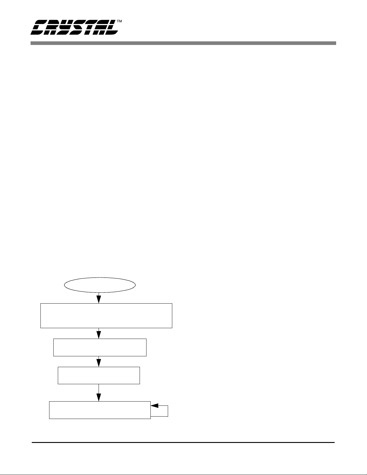
SOFTWARE DESCRIPTION
This note presents algorithms to initialize the
68HC05 and the CS5525/6/9, perform a self-offset
calibration, modify the CS5525/6/9’s gain register,
and acquir e a c onversi on. Fi gure 2 depi cts a block
CS5525/6/9 68HC05
CS
SDI
SDO
SCLK
Cirrus Logic, Inc.
Crystal Semiconductor Products Division
P.O. Box 17847, Austin, Texas 78760
(512) 445 7222 FAX: (512) 445 7581
http://www.crystal.com
No Connect
MOSI (PD3)
MISO (PD2)
SCK(PD4)
Figure 1. 3-Wire and 4-Wire Interfaces
CS5525/6/9 68HC05
CS
SDI
SDO
SCLK
Copyright Cirrus Logic, I nc. 1997
(All Rights Reserv ed)
PA0
MOSI (PD3)
MISO (PD2)
SCK (PD4)
NOV ‘97
AN89Rev2
1
Page 2
AN89
diagram. While reading this application note,
please refer to the Appendix for the code listing.
Initialize
Initialize is a subrout in e tha t con fig ures th e SPI
TM
on the 68HC05 and pl aces the CS5525/6/9 in the
command-state. Figure 1 d epi cts how the interface
is configured (for more information on configuring
TM
the SPI
tion Guide) . Afte r confi gurin g t he SP I
refer to Moto rol a’s M68HC 05 Applic a-
TM
, the con troller enters a delay state to allow time for the
CS5525/6/9’s power-on-reset and oscillator to
start-up (oscillator start-up time is typically 500
mS). The last step is to reinitialize the serial port on
the ADC (r einitializing t he serial port is unnecessary here, the code was added for demonstration
purposes only). This is implemented by sending the
converter sixteen bytes of logic 1’s followed by one
final byte, with its LSB at logic 0. Once sent, the sequence plac es the serial port of the ADC int o the
command-state, where it aw aits a valid co mman d .
After returning to main, the software demo nstrates
how to calibra te the convert er’s offset.
START
INITIALIZE
MICROCONTROLLER & CS5525/6/9
SELF-OFFSET CAL.
Self-Offset Calibratio n
Calibrate is a subroutine that calibrates the converter’s offset. Calibrate first sends 0x000001
(Hex) to the conf iguration register. This i nstructs
the converter to perform a self-offset calibration.
Then the Done Flag (D F) bit in th e configuration
register i s polled until set. Onc e DF is set, it indicates that a val id c al ibration is perform ed. To minimize digi tal n oise (whil e perf ormin g a cal ibrat ion
or a conversio n), m any syste m d esigners m ay f ind
it advantage ous to add a software delay e qui va lent
to a convers ion or calib ration cy cle before po lling
the DF bit.
Read/Write Gain Register
To modify the gain register the command-byte and
data-byte variables are first initialized. This is accomplis hed with the LDA and S TA opcode s. The
subroutine write_register u ses t hese va riables to set
the conte nts of the gain re gister in the C S552 5/ 6/9
to 0x800000 (HEX). To do this, write_register
calls send_spi four tim es (once fo r the command -
byte and three additional times for the 24 bits of data). Send_spi is a subroutine used to transfer a byte
of informatio n fro m th e 68HC0 5 t o the CS5525/ 6/
TM
9 via the SPI
. A byte is transferred on e bit at a
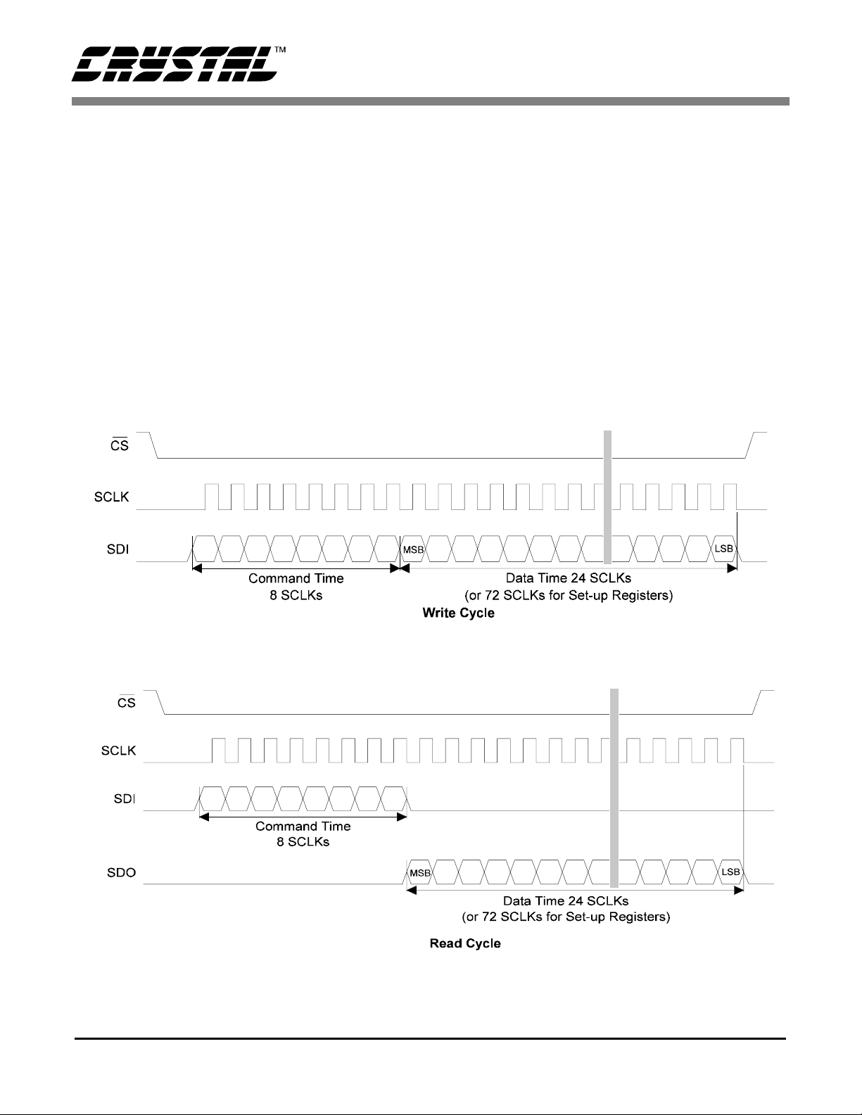
time, MSB (most significant bit) fi rst. Figure 3 depicts the timi ng diagram for the write-cy cle in the
CS5525/6/9’s serial port. This algorithm demonstrates how to write to the gai n register. It does not
perform a ga in calibrati on. T o perform a gain calibration, follo w the procedu res outlined in th e data
sheet.
To verify if 0x800000(HEX) was written to the
MODIFY GAIN
gain register, read_register is call ed. It dup licates
the read-cycle timing diagram depicted in Figure 4.
Read_register calls send_spi once to transfer the
command-byt e to the CS5525/ 6/9. This place s the
ACQUIRE CONVERSION
converter into the data-state where it waits until
data is read from its serial port. Read_reg ister calls
Figure 2. CS5525/6/9 Software Flowchart
2 AN89Rev2
receive_spi three times and tra ns f ers three bytes o f
Page 3
AN89
information from the CS5525/6/9 to the 68HC05
TM
via the SPI
. Similar to send_spi, receive_spi receives a byte one bit at a time MSB first. When the
transfer is complete , highbyte, midbyte, and low-
byte byte contain the CS5525/6/9’s 24-bit gain register.
Acquire Conversion
To acquire a c onversion the subroutine convert is
called. Convert se nds the command-byte 0x0 C to
the converter instructing it to perform a single conversion. Th en the Done Flag bit in th e configuration registe r is polle d. When D F is set , it indica tes
that a conversion was performed. The 68HC05 then
reads the conversion data register to acquire the
conversion. Figu re 6 dep ic ts ho w 16-bit and 20-bit
conversion words are stored in the 68HC05.
An alternate m ethod ca n be used to acquire a conversion. By se tting the Port Flag bit (PF, the fifth
bit in the configuration register), SDO’s function is
modified to fall to logic 0 when a conversion is
complete (refer to Fi gure 5). By tying SDO t o the
controller’s interrupt pin, conversions can be acquired via an interrupt service routine.
Figure 3. Write-Cycle Timing
Figure 4. Read-Cycle Timing
AN89Rev2 3
Page 4
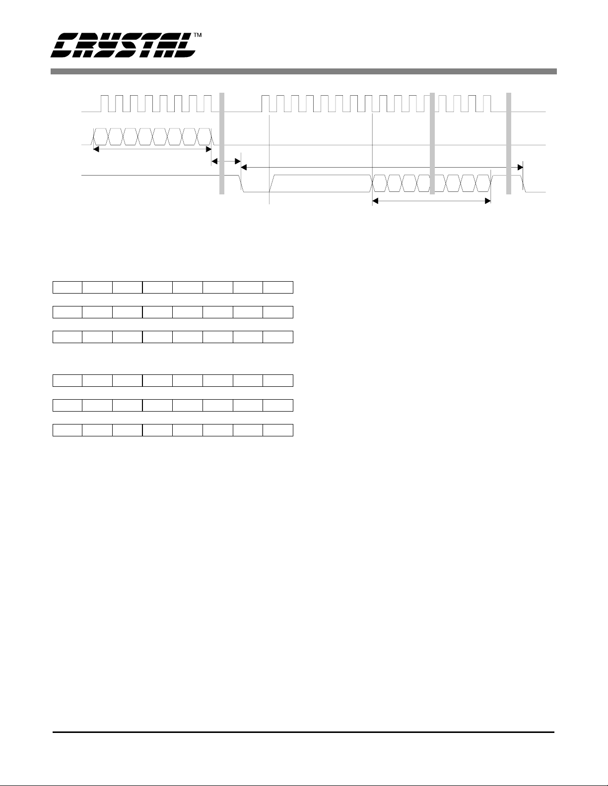
SCLK
SDI
*
t
ommand Time
C
8SCLKs
DO
S
td = XIN/O WR clock cycles for e ach conversion except t he
*
first conversion whichwilltakeXIN/OWR+ 7 clockcycles
Figure 5. Conversion/Acquisition Cycle with the PF Bit Asserted
.MSB High-Byte
D19 D18 D17 D16 D15 D14 D13 D12
Mid-Byte
D11 D10 D9 D8 D7 D6 D5 D4
Low-Byte
D3 D2 D1 D0 0 0 OD OF
A) 20-Bit Conversion Data Word
MSB High-Byte
D15 D14 D13 D12 D11 D10 D9 D8
Mid-Byte
D7 D6 D5 D4 D3 D2 D1 D0
Low-Byte
111100ODOF
B) 16-Bit Conversion Data Word
0- always zero, 1
OD - Oscillation Detect, OF - Overflow
Figure 6. Bit Representation/Storage in 68HC05
- always one,
d
SCLKs Clear SDO Flag
8
Data SDO Continuous Conversi on Read (PF bit = 1)
MAXIMUM SCLK RATE
A machine cy c le in the 68HC05 consists 2 oscill a-
tor periods or 500 ns if t h e m i crocontrolle r’s osc il lator freq uency i s 4 MHz. Since t he CS 5525/6/9 ’s
maximum SCLK rate i s 2MHz, addi ti onal no ope ration (NOP) delays may be necessary to reduce the
AN89
IN/OWR
X
Clock Cycles
SB
M
ataTime
D
24 SCLKs
transfer rate if the mic rocon troller system re quires
higher rate oscillators.
CONCLUSION
This applicat ion note pre sents an exam ple of how
to interface the CS5525/6/9 to the 68HC05. It is divided into tw o main sections: hardware and software. The hardware section illustrates both a threewire and a f our-wire interfac e. The three-wi re in-
TM
terface is SPI
and MICROWIR E
The software section il lustrate s how to initia lize the
converter and microcontroller, calibrate the converters offset, write to and read from the ADC’s internal register, and acquire a conversion. The
software is modularized and illustrates important
subroutines, e .g. wr ite_ regi ste r and read _register.
The software desc ribed in this note is included in
the Appendix at the end of t his document.
TM
SPI
MICROWIRE
is a trademark of Motorola.
TM
is a tradem ark of Nati onal Sem i-
conductor.
SB
L
TM
compatible.
4 AN89Rev2
Page 5

APPENDIX
68HC05 Microcode to Interface to the CS5525/6/9
****************************************************************************
*
* File: 55266805.asm
* Date: November 1, 1996
* Programmer: Keith Coffey
* Revision: 0
*
* Processor: 68HC05
*
* Program entry point at routine "main". The entry point is address $100
****************************************************************************
*
* This program is designed as an example of interfacing a 68HC05 to a CS5525/6/9
* ADC. The program interfaces via SPI (i.e. port D) which controls the
* serial communications, calibration, and conversion signals. Other ADC’s
* (16-bit and 20-bit) in the product family can be used.
****************************************************************************
******** Memory Map Equates
PORTA EQU $00 ; General Purpose I/O Port
DDRA EQU $04 ; Data Direction Control For Port A
SPCR EQU $0A ; Serial Peripheral Control Register
SPSR EQU $0B ; Serial Peripheral Status Register
SPDR EQU $0C ; Serial Peripheral Data I/O Register
SPIF EQU 7 ; Serial Peripheral Data Transfer Flag
******** RAM Values
ORG $50
******** Ram Memory Equates
HIGHBYTE RMB 1 ; Upper 8 bits of Conversion Register
MIDBYTE RMB 1 ; Middle 8 bits of Conversion Register
LOWBYTE RMB 1 ; Lowest 8 Bits of Conversion Register
COMMANDBYTE RMB 1 ; One byte RAM storage location
AN89
AN89Rev2 5
Page 6

**************************************************************************************
* Program Code
**************************************************************************************
ORG $0100
**************************************************************************************
* Routine - Main
* Input - none
* Output - none
* This is the entry point to the progr am.
**************************************************************************************
MAIN EQU * ; Start from Reset Vector
******** Initialize System and Perform SELF OFFSET Calibration
JSR initialize ; Initial ize the sys tem
JSR calibrate ; Calibrate the ADC Offset
******** Write to the GAIN Register
LDA #$82 ; Prepare COMMANDBYTE
STA COMMANDBYTE
LDA #$80 ; Prepare HIGHBYTE
STA HIGHBYTE
CLR MIDBYTE ; Prepare MIDBYTE
CLR LOWBYTE ; Prepare LOWBYTE
JSR write_register ; Write to Gain Register
******** Read from the GAIN Register
LDA #$92 ; Prepare COMMANDBYTE
STA COMMANDBYTE
JSR read_register ; Read the Gain Register
******** Perform Single Conversions
LOOP JSR convert ; Convert Analog input
JMP LOOP ; Repeat Loop
******** End MAIN
AN89
6 AN89Rev2
Page 7

**************************************************************************************
* Subroutines
**************************************************************************************
**************************************************************************************
* Routine - initialize
* Input - none
* Output - none
* This subroutine initializes port D for interfacing to the CS5525/6/9 ADC.
* It provides a time delay for oscillator start-up/wake-up period.
* A typical start-up time for a 32768 Hz crystal, due to high Q, is 500 ms.
* Also 1003 XIN clock cycles are allotted for the ADC’s power on reset.
**************************************************************************************
initialize LDA #%01010000 ; Load ACCA with for SPSC
STA SPCR ; Setup SPI
LDA #40 ; Load ACCA with delay count
JSR delay ; Delay, Power on Reset 1003 XIN
LDA #220 ; Load ACCA with delay count
JSR delay ; Delay, Oscillator start-up 170 mS
JSR delay ; Delay, Oscillator start-up 170 mS
JSR delay ; Delay, Oscillator start-up 170 mS
LDX #$0F ; Reset Serial Port on ADC
LDA #$FF ; Load ACCA with $FF
loop JSR send_spi ; Move $FF to SPDR
DECX ; Decrement the counter
BNE loop ; Repeat loop is counter not zero
LDA #%11111110 ; Load ACCA with last byte
JSR send_spi ; Move $FE to SPDR
RTS ; Exit subroutine
**************************************************************************************
* Routine - calibrate
* Input - none
* Output - none
* This subroutine instructs the CS5525/6/9 to perform self-calibration.
**************************************************************************************
calibrate LDA #$84 ; set command byte for config write
STA COMMANDBYTE ; set COMMAND BYTE
CLR HIGHBYTE ; clear HIGHBYTE
CLR MIDBYTE ; clear MIDBYTE
LDA #$01 ; get ready for self offset cal
STA LOWBYTE ; set LOWBYTE
JSR write_register ; Write to Config Register
AN89
LDA #$94 ; set command byte for config read
STA COMMANDBYTE ; set COMMAND BYTE
poll_done: JSR read_register ; Poll done flag until cal complete
BRCLR 3,LOWBYTE,poll_done; repeat if flag not set
RTS ; Exit subroutine
AN89Rev2 7
Page 8

**************************************************************************************
* Routine - convert
* Input - none
* Output - Conversion results in memory locations HIGHBYTE, MIDBYTE and
* LOWBYTE. This algorithm performs only single conversions. If
* continuous conversions are needed the routine needs to be
* modified. Port flag is zero.
*
* HIGHBYTE MIDBYTE LOWBYTE
* 7 6 5 4 3 2 1 0 7 6 5 4 3 2 1 0 7 6 5 4 3 2 1 0
* 16-bit results MSB LSB 1 1 1 1 0 0 OD OF
* 20-bit results MSB LSB 0 0 OD OF
* This subroutine initiates a single conversion.
**************************************************************************************
convert LDA #$C0 ; Set COMMANDBYTE for single CONV
STA COMM ANDBYTE
JSR send_spi ; Transmit command out SPI
LDA #$94 ; Set command byte for config read
STA COMM ANDBYTE ; Send COMMAND BYTE
done1 JSR read_register ; Poll done flag until CONV complete
BRCLR 3,LOWBYTE,done1 ; Repeat if Done Flag not Set
AN89
LDA #$96 ; Set Byte to Read Conversion Reg.
STA COMM ANDBYTE ; Store COMMAND BYTE
JSR read_register ; Acquire the Conv ersion
RTS ; Exit subroutine
**************************************************************************************
* Routine - write_register
* Input - COMMANDBYTE, HIGHBYTE, MIDBYTE, LOWBYTE
* Output - none
* This subroutine instructs the CS5525/6/9 to write to an internal register.
**************************************************************************************
write_register LDA C OMMANDBYTE ; Load ACCA with COMMANDBYTE
JSR send_spi ; transfer byte
LDA HIGHBYTE ; Load ACCA with HIGHBYTE
JSR send_spi ; transfer byte
LDA MIDBYTE ; Load ACCA with MIDBYTE
JSR send_spi ; transfer byte
LDA LOWBYTE ; Load ACCA with LOWBYTE
JSR send_spi ; transfer byte
RTS ; Exit Subroutine
8 AN89Rev2
Page 9

**************************************************************************************
* Routine - read_register
* Input - COMMANDBYTE
* Output - HIGHBYTE, MIDBYTE, LOWBYTE
*
* This subroutine reads an internal register of the ADC.
**************************************************************************************
read_register LDA COMM ANDBYTE ; Load ACCA with COMMANDBYTE
JSR send_spi ; transfer byte
JSR receive_spi ; receive byte
STA HIGHBYTE ; Move ACCA with HIGHBYTE
JSR receive_spi ; receive byte
STA MIDBYTE ; Move ACCA with MIDBYTE
JSR receive_spi ; receive byte
STA LOWBYTE ; Move ACCA with LOWBYTE
RTS ; Exit Subroutine
**************************************************************************************
* Routine - send_spi
* Input - Byte to be transmitted is placed in ACCA
* Output - none
*
* This subroutine sends a byte to the ADC.
**************************************************************************************
send_spi: STA SPDR ; Move ACCA to SPDR
wait0 BRCLR SPIF,SPSR,wait0 ; Loop until byte is transmitted
RTS ; Exit Subroutine
AN89
**************************************************************************************
* Routine - receive_spi
* Input - none
* Output - Byte received is placed in ACCA
* This subroutine receives a byte from the ADC.
**************************************************************************************
receive_spi: CLRA ; Load ACCA register with Zero
STA SPDR ; Initiate a transfer of all Zero’s
wait1 BRCLR SPIF,SPSR,wait1 ; Reset Flag SPIF bit
LDA SPDR ; Move SPDR to ACCA
RTS ; Exit Subroutine
AN89Rev2 9
Page 10

**************************************************************************************
* Routine - delay
* Input - Count in register A
* Output - none
*
* This subroutine delays by using count from register A. The 68HC05
* development board uses a 4.0MHz clock (E = 2.0 MHz), thus each cycle is
* 500 nS. This delay is equivalent to (500ns)*(1545)*(count value),
* (a count of 720 provides a 556ms delay).
**************************************************************************************
delay
outlp CLRX ; X used as inner loop count
innlp DECX ; 0-FF, FF-FE, FE-FD, ....1-0 256 loops
NOP ; 2 cycles
NOP ; 2 cycles
BNE innlp ; 10 cycles*256*500ns=1.28 ms
DECA ; Countdown the ac cumulator
BNE outlp ; 2569 cycles*500ns*A
RTS ; Exit subroutine
AN89
**************************************************************************************
* Interrupt Vectors
**************************************************************************************
NOT_USED RTI
ORG $1FF4 ; Interrupt Vectors
FDB NOT_USED ; SPI Interrupt
FDB NOT_USED ; SCI Interrupt
FDB NOT_USED ; Timer Interrupt
FDB NOT_USED ; IRQ Interrupt
FDB NOT_USED ; SWI Interrupt
FDB MAIN ; Reset interrupt- power on reset
10 AN89Rev2
Page 11

• Notes •
Page 12

 Loading...