

Page 1

Application Note
Interfacing the CS5525/6/9 to the PIC16F84
By Keith Coffey
AN88
INTRODUCTION
This applica tion note details the interfac e of Crys-
tal Semiconductor’s CS5525/6/9 Analog-to-Digital Converter (ADC) to the Microchip PIC16
microcontroller series. This note takes the reader
through a sim ple e xa mpl e desc ribin g h ow to co mmunicate w ith the ADC. All algo rithms discussed
are included in the Appendix at the end of this
note.
ADC DIGITAL INTERFACE
The CS5525/6/9 interfaces to the PIC16F84
through either a three-wire or a four-wire interface.
Figure 1 depict s the inte rface be tween the two devices. Though this software was written to interface to Port A (RA) on th e PIC16F 84 with a four wire interfa ce, the algorit hms can be easily modified to work with the three-wire format.
The ADC’s serial port consists of four control
lines: CS
CS
, SCLK, SDI, and SDO.
, Chip S elect, is the contro l line w hich e nables
access to the serial port.
SCLK, Serial Clock, is the bit-clock which controls
the shifting of data to or from the ADC’s serial
port.
SDI, Serial Data In, is the data signal used to transfer data from the PIC16F84 to the ADC.
SDO, Serial Data Out, is the data signal used to
transfer output data from the ADC to the
PIC16F84.
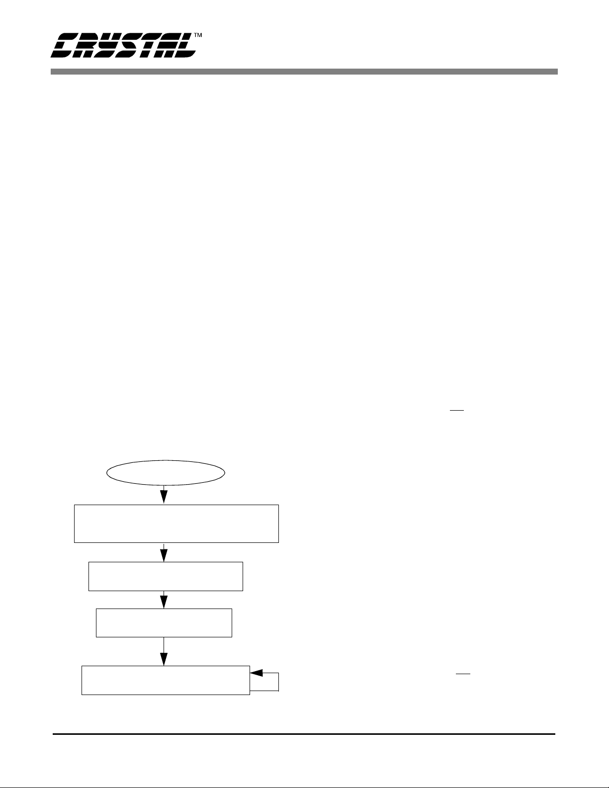
SOFTWARE DESCRIPTION
This note presents algorithms to initialize the
PIC16F84 and the CS5525/6/9, perform a se l f-offset calibratio n, modi fy the C S5525/ 6/9 gai n register, and then acquire a conversion. Figure 2 depicts
CS5525/6/9 PIC16F84
CS
SDI
SDO
SCLK
Cirrus Logic, Inc.
Crystal Semiconductor Products Division
P.O. Box 17847, Austin, Texas 78760
(512) 445 7222 FAX: (512) 445 7581
http://www.crystal.com
NC (RA0)
RA1
RA2
RA3
Figure 1. 3-Wire and 4-Wire Interfaces
CS5525/6/9 PIC16F84
CS
SDI
SDO
SCLK
Copyright Cirrus Logic, I nc. 1997
(All Rights Reserv ed)
RA0
RA1
RA2
RA3
NOV ‘97
AN88Rev2
1
Page 2
AN88
a block diagra m overview. While readi ng this application note, please refer to the Appendix for the
code listing.
Initialize
Initialize is a subroutine that configures Port A
(RA) on the PIC1 6F84 a nd place s the C S5525/ 6/9
in the command-state. First, RA’s data direction is
configured as dep ic te d i n Figure 1 (for more infor mation on configuring ports refer to Microchip’s
PIC16F8X Data Sheet). After configuring the port,
the control ler en te rs a de lay st ate t o al low tim e fo r
the CS5525/6 /9’s power-on-re set and oscillato r to
start-up (oscillator start-up time is typically 500
ms). The last step is to reinitialize the serial port on
the ADC (r einitializing t he serial port is unnecessary here, it was added for demonstration purposes
only). This is implemented by sending the converter sixteen byte s of logic 1’s foll owed by one fin al
byte, with its LSB logic 0. Once sent, the sequence
places the serial port of the ADC into the command-state, where it aw aits a valid command.
After returning to main, the software demo nstrates
how to calibra te the convert er’s offset.
START
INITIALIZE
MICROCONTROLLER/CS5525/6/9
SELF-OFFSET CAL.
MODIFY GAIN
ACQUIRE CONVERSION
Figure 2. CS5525/6/9 Software Flowchart
Self-Offset Calib r ation
Calibrate is a subroutine that calibrates the converter’s offset. Calibrate first sends 0x000001
(Hex) to the conf iguration register. This i nstructs
the converter to perform a self-offset calibration.
Then the Done Flag (D F) bit in th e configuration
register i s polled until set. Onc e DF is set, it indicates that a valid calibration was performed. To
minimize digital noise (while performing a calibration or a c onver sion ), ma ny sy ste m d esigners may
find it advantageous to add a software delay equivalent to a conversion or calibration cycle before
polling the DF bit.
Read/Write Gain Register
To modify the gain register the command-byte and
data-byte variables are first initialized. This is accomplished by the MOVLW and MOVWF opcodes. The subroutine write_register uses these
variables to set th e conten ts of the gain regi ster in
the CS5525/6/9 to 0x800000 (HEX). To do this,
write_register first asserts CS
and then it calls
send_spi four times (once for the command-byte
and three a dditional times for t he 24 bit s of data).
Send_spi is a subroutine used to ‘bit-bang’ a byte of
information from the PIC16F84 to the CS5525/6/9.
A byte is tra nsferre d one bit at a time , MSB (most
significan t bit) first, by placing an info rmation b it
on RA1 (SDI) and then pulsing RA3 (SCLK). This
process is repeated eight times. Figure 3 depicts the
timing diag ram for t he write-c ycle in the CS5525/
6/9’s serial port. Th is al gorit hm de mo nstrat es how
to write to the g ain register . It doe s not pe rform a
gain calibration. To perform a gain calibration, follow the procedu r es ou tlined in the data shee t.
To verify if 0x800000 (HEX) was written to the
gain register, read_register is call ed. It dup licates
the read-cycle timing diagram depicted in Figure 4.
Read_register first asserts CS
and then calls
send_spi once to transfe r the com ma nd- byte to the
CS5525/6/9. This places the converter into the
2 AN88Rev2
Page 3
AN88
data-state where it wa its unt il data is rea d from its
serial port. To re ceiv e th e da ta, read_register ca ll s
receive_spi th ree times. Receive_sp i is a subroutine
used to ‘bit-ba ng’ a byte of informa tion from the
ADC to the PIC16F84. Similar to send_spi,
receive_spi acquires this information one bit at a
time MSB first. When the transfer is complete, the
variables high byte, midbyte, and lowbyte contain
the CS5525/6/ 9’s 24-bit gain registe r.
Acquire Conversion
To acquire a c onversion the subroutine convert is
called. Convert se nds the command-byte 0x0 C to
the convert er. This instructs the converter to perform a single conversion. Then the Done Flag (DF)
bit in the configuration register is polled. When set,
DF indicates that a conversion was performed.
Once DF is s et, the cont roller reads the conve rs ion
data register to acquire the conversion.Figure 6 depicts how 16-bit and 2 0-bit conversion words are
stored in th e microcontroller.
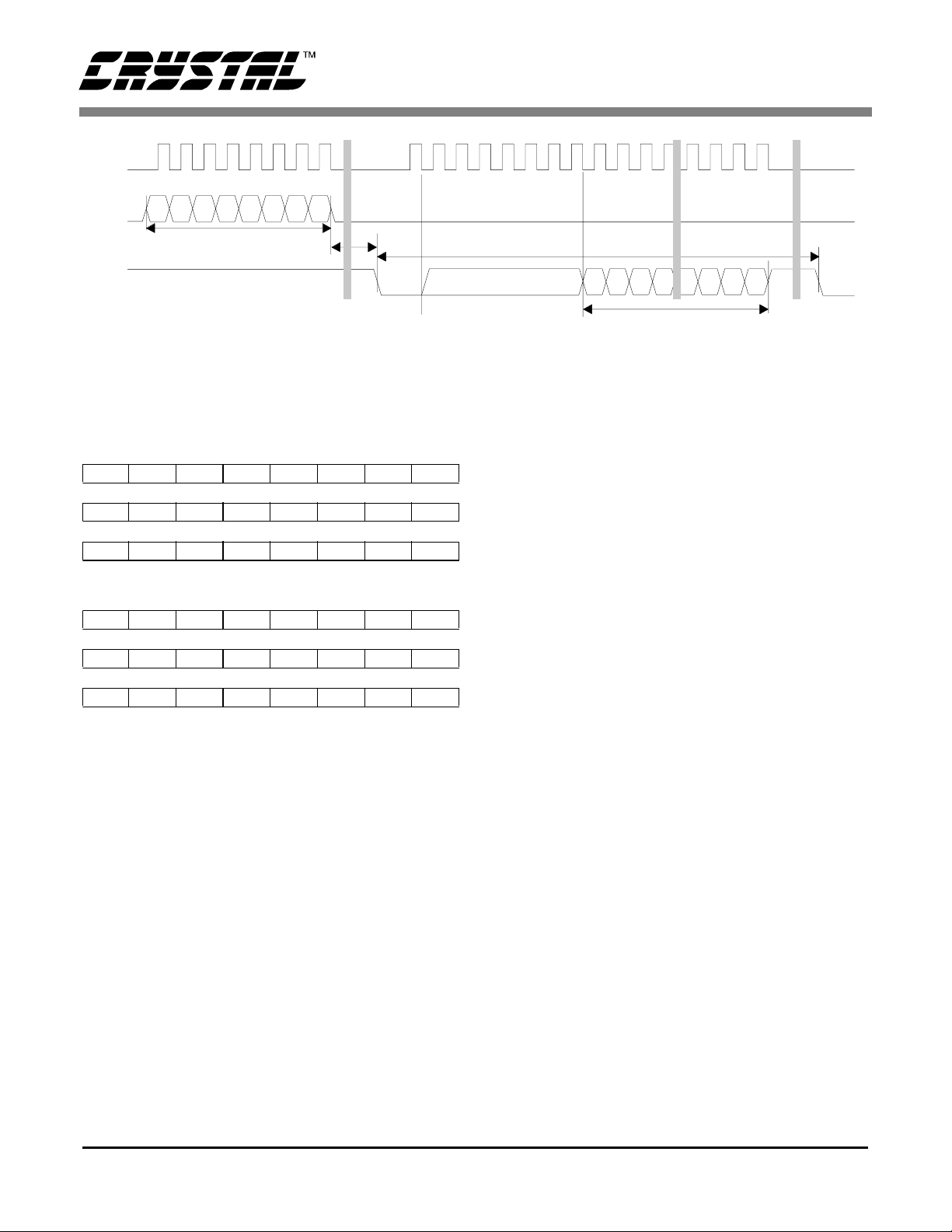
An alternate m ethod ca n be used to acquire a conversion. By se tting the Port Flag bit (PF, the fifth
bit in the configuration register), SDO’s function is
modified to fall to logic 0 when a conversion is
complete (refer to Fi gure 5). By tying SDO t o the
controller’s interrupt pin, conversions can be acquired via an interrupt service routine.
Figure 3. Write-Cycle Timing
Figure 4. Read-Cycle Timing
AN88Rev2 3
Page 4
SCLK
SDI
*
t
ommand Time
C
8SCLKs
DO
S
td = XIN/OWR clock cycles for each conversion except the
*
first conversion whichwilltakeXIN/OWR+ 7 clockcycles
Figure 5. Conversion/Acquisition Cycle with the PF Bit Asserted
d
Data SDO Continuous Conversion Read (PF bit = 1)
SCLKs Clear SDO Flag
8
AN88
IN/OWR
X
Clock Cycles
SB
M
ataTime
D
24 SCLKs
SB
L
MSB High-Byte
D19 D18 D17 D16 D15 D14 D13 D12
Mid-Byte
D11 D10 D9 D8 D7 D6 D5 D4
Low-Byte
D3 D2 D1 D0 0 0 OD OF
A) 20-Bit Conversion Data Word
MSB High-Byte
D15 D14 D13 D12 D11 D10 D9 D8
Mid-Byte
D7 D6 D5 D4 D3 D2 D1 D0
Low-Byte
111100ODOF
B) 16-Bit Conversion Data Word
0- always zero, 1
OD - Oscillation Detect, OF - Overflow
Figure 6. Bit Representation/Storage in PIC16F84
- always one,
MAXIMUM SCLK RATE
A machine cyc le in the PIC16F84 c onsists 4 oscil-
lator periods o r 400 ns i f the mic rocontrol ler’s os cillator frequency is 10 MHz. Sinc e the CS5525/6/
9’s maximum SCLK ra te is 2MHz, additiona l no
operation (NOP) delays may be necessary to reduce the tr ansfer rate if the micro controller s ys tem
requires higher ra te oscillators.
SERIAL PERIPHERAL INTERFACE
The Serial Peripheral Interface (SPI) developed for
Microchip’s controllers wasn’t designed to be as
flexible as the SPI port on Motorola’s 68HC05. To
get the Micr ochip’s SPI port to functi on with the
CS5525/6/9, th e port n ee ds to be ini tia lized t o id le
high, and th e CS55 25/6/9’s se rial po rt needs to be
reset anytime information is transmitted between
the microcontroller and th e c onverter.
DEVELOPMENT TOOL DESCRIPTION
The code in this a ppl ication note was developed
TM
using MPLAB
development pa cka ge from Microchip, Inc .
4 AN88Rev2
, an integrated software
Page 5

AN88
CONCLUSION
This applicat ion note prese nts an example of how
to interface t he CS5525/6/9 to the PIC16 F84. It is
divided into two main sec ti ons: har dware and software. The hardware section illustrates both a threewire and a four-wire interface. The three-wire is
TM
SPI
and MICROWIRE
ware, develope d w ith dev elopme nt to ols fro m Microchip, Inc., illustrates how to initialize the
converter and microcontroller, calibrate the con-
TM
compat ible. The soft-
verters offset, write to and read from the ADC’s internal register, and acquire a conversion. The
software is modularized and illustrates important
subroutines, e .g. wr ite_ regi ste r and read _register.
The softwa re described in the no te is included in
the Appendix at the end of this do cument.
SPITM is a trademark of Motorola.
MICROWIRE
MPLAB
TM
is a trademark of National Semiconductor.
TM
is a trademark of Microchip.
AN88Rev2 5
Page 6

APPENDIX
PIC16F84 Microcode to Interface to the CS552 5/ 6/9
;*************************************************************************************
;* File: 55261684.asm
;* Date: November 15, 1996
;* Programmer:Keith Coffey
;* Revision: 0
;* Processor: PIC16F84
;* Program entry point at routine "main". The entry point is address 0x05.
;*************************************************************************************
;* Program is designed as an example to interface a PIC16F84 to a CS5525/6/9
;* ADC. The program interfaces via a software SPI which controls the
;* serial communications, calibration, and conversion signals. Other ADC’s
;* (16-bit and 20-bit) in the product family can be used.
;*************************************************************************************
;******** Memory Map Equates
INDF equ 0x00 ; Indirect Address Register
STATUS equ 0x03 ; STATUS register equate
FSR equ 0x04 ; File Select Register
PORTA equ 0x05 ; General Purpose I/O Port
TRISA equ 0x85 ; Data Direction Control For Port A
RP0 equ 0x05 ; Register Bank Select Bit
CS equ 0x00 ; Port A bit 0
SDI equ 0x01 ; Port A bit 1
SDO equ 0x02 ; Port A bit 2
SCLK equ 0x03 ; Port A bit 3
LED equ 0x04 ; Port A bit 4
TRUE equ 0x01 ; Represents logic 1
HIGHBYTE equ 0x0C ; Upper 8 bits of Conversion Register
MIDBYTE equ 0x0D ; Middle 8 bits of Conversion Register
LOWBYTE equ 0x0E ; Lowest 8 Bits of Conversion Register
COMMANDBYTE equ 0x0F ; One byte RAM storage location
TEMP equ 0x10 ; A Temporary Data Storage Register
COUNT equ 0x11 ; Used to store count for delay routine
SPDR equ 0x12 ; Reserved for Se rial Peri pheral D ata Reg.
CARRY_BIT equ 0x00 ; Represents the Carry Bit in Status Reg.
AN88
6 AN88Rev2
Page 7

;*************************************************************************************
;* Program Code
;*************************************************************************************
processor 16C84 ; Set Processor Type
org 0x00 ; Reset Vector
goto Main ; Start at Main
;*************************************************************************************
;* Routine - Main
;* Input - none
;* Output - none
;* This is the entry point to the program.
;*************************************************************************************
org 0x05
Main ; Start fr om Reset Vector
;******** Initialize System and Perform SELF OFFSET Calibration
CALL initiali ze ; Initialize the syste m
CALL calibrate ; Calibrate the ADC Offset
;******** Write to the GAIN Register
MOVLW 0x82 ; Prepare COMMANDBYTE
MOVWF COMMANDBYTE
MOVLW 0x80 ; Prepare HIGHBYTE
MOVWF HIGHBYTE
CLRF MI DBYTE ; Prepare MIDBYTE
CLRF LOWBYTE ; Prepare LOWBYTE
CALL write_register ; Write to Gain Register
;******** Read from the GAIN Register
MOVLW 0x92 ; Prepare COMMANDBYTE
MOVWF COMMANDBYTE
CALL read_register ; Read the Gain Register
;******** Perform Single Conversions
LOOP CALL convert ; Convert Analog input
goto LOOP ; Repeat Loop
;******** End MAIN
AN88
AN88Rev2 7
Page 8

;*************************************************************************************
;* Subroutines
;*************************************************************************************
;*************************************************************************************
;* Routine - initialize
;* Input - none
;* Output - none
;* This subroutine initializes port A for interfacing to the CS5525/6/9 ADC.
;* It provides a time delay for oscillator start-up/wake-up period.
;* A typical start-up time for a 32768 Hz crystal, due to high Q, is 500 ms.
;* Also 1003 XIN clock cycles are allotted for the ADC’s power on reset. The
;* total delay is 555 ms upon power-up (assume uC start-up time is zero).
;*************************************************************************************
initiali ze CLRF PORTA ; Initialize POR TA by setting output
; data latches.
BSF STATUS, RP0 ; Select Bank 1
MOVLW 0x04 ; Value used to initialize direction
MOVWF TRISA ; Set RA2 as inputs
; RA0, RA1, RA3, & RA4 as outputs
AN88
BCF STATUS, RP0 ; Select Bank 0
BCF PORTA,SDO ; Clear SDO
MOVLW 0x32 ; Load W with delay count
CALL delay ; Delay, Power on Reset 1003 XIN
MOVLW 0xFF ; Load W with delay count
CALL delay ; Delay, Oscillator start-up 158 ms
CALL delay ; Delay, Oscillator start-up 158 ms
CALL delay ; Delay, Oscillator start-up 158 ms
CALL delay ; Delay, Oscillator start-up 158 ms
MOVLW 0x0F ; Reset Serial Port on ADC
MOVWF TEMP
BCF PORTA,CS ; Clear CS
loop MOVLW 0xFF ; Load W with 0xFF
CALL send_spi ; Send 15 0xFF through SPI
DECFSZ TEMP,1 ; Decre ment the c ounter
goto loop ; Repeat loop if counter not zero
MOVLW 0xFE ; Load W with last byte
CALL send_spi ; Move 0xFE to SPDR
BSF PORTA,CS ; Clear CS
RETURN ; Exit subroutine
8 AN88Rev2
Page 9

;*************************************************************************************
;* Routine - calibrate
;* Input - none
;* Output - none
;* This subroutine instructs the CS5525/6/9 to perform self-offset calibration.
;*************************************************************************************
calibrate MOVLW 0x84 ; set command byte for config write
MOVWF COMMANDBYTE ; set COMMAND BYTE
CLRF HIGHBYTE ; clear HIGHBYTE
CLRF MIDBYTE ; clear MIDBYTE
MOVLW 0x01 ; get ready for self offset cal
MOVWF LOWBYTE ; set LOWBYTE
CALL write_register ; Write to Config Register
MOVLW 0x94 ; set command byte for config read
MOVWF COMMANDBYTE ; set COMMAND BYTE
poll_done: CALL read_register ; Poll done flag until cal complete
BTFSS LOWBYTE,3 ; repeat if flag not set
goto poll_done
RETURN ; Exit subroutine
AN88
;*************************************************************************************
;* Routine - convert
;* Input - none
;* Output - Conversion results in memory locations HIGHBYTE, MIDBYTE and
;* LOWBYTE. This algorithm performs only single conversions. If
;* continuous conversions are needed the routine needs to be
;* modified. Port flag is zero.
;* HIGHBYTE MIDBYTE LOWBYTE
;* 7 6 5 4 3 2 1 0 7 6 5 4 3 2 1 0 7 6 5 4 3 2 1 0
;* 16-bit results MSB LSB 1 1 1 1 0 0 OD OF
;* 20-bit results MSB LSB 0 0 OD OF
;* This subroutine initiates a single conversion.
;*************************************************************************************
convert MOVLW 0xC0 ; Set COMMANDBYTE for single CONV
MOVWF COMMANDBYTE
BCF PORTA,CS ; Clear Chip Select
CALL send_spi ; Transmit command out SPI
MOVLW 0x94 ; Set command byte for config read
MOVWF COMMANDBYTE ; Send COMMAND BYTE
done1 CALL read_register ; Poll done flag until CONV complete
BTFSS LOWBYTE,3 ; Repeat if Done Flag not Set
goto done1
MOVLW 0x96 ; Set Byte to Read Conversion Reg.
MOVWF COMMANDBYTE ; Store COMMAND BYTE
CALL read_register ; Acquire the Conversion
BSF PORTA,CS ; Set Chip Select
RETURN ; Exit subroutine
AN88Rev2 9
Page 10

;*************************************************************************************
;* Routine - write_re gister
;* Input - COMMANDBYTE, HIGHBYTE, MIDBYTE, LOWBYTE
;* Output - none
;*
;* This subroutine instructs the CS5525/6/9 to write to an internal register.
;*************************************************************************************
write_register BCF PORTA,CS ; Clear Chip Select
MOVF COMMANDBYTE,0 ; Load W with COMMANDBYTE
CALL send_spi ; transfer byte
MOVF HIGHBYTE,0 ; Load W with HIGHBYTE
CALL send_spi ; transfer byte
MOVF MIDBYTE,0 ; Load W with MIDBYTE
CALL send_spi ; transfer byte
MOVF LOWBYTE,0 ; Load W with LOWBYTE
CALL send_spi ; transfer byte
BSF PORTA,CS ; Set Chip Select
RETURN ; Exit Subroutine
AN88
;*************************************************************************************
;* Routine - read_register
;* Input - COMMANDBYTE
;* Output - HIGHBYTE, MIDBYTE, LOWBYTE
;* This subroutine reads an internal register of the ADC.
;*************************************************************************************
read_register BCF PORTA,CS ; Clear Chip Select
MOVF COMMANDBYTE,0 ; Load W with COMMANDBYTE
CALL send_spi ; transfer byte
CALL receive_spi ; receive byte
MOVWF HIGHBYTE ; Move W to HIGHBYTE
CALL receive_spi ; receive byte
MOVWF MI DBYTE ; Move W to MIDBYTE
CALL receive_spi ; receive byte
MOVWF LOWBYTE ; Move W to LOWBYTE
BSF PORTA,CS ; Set Chip Select
RETURN ; Exit Subroutine
10 AN88Rev2
Page 11

;*************************************************************************************
;* Routine - send_spi
;* Input - Byte to be transmitted is placed in W
;* Output - None
;* This subroutine sends a byte to the ADC.
;*************************************************************************************
send_spi: MOVWF SPDR ; Move W to SPDR
MOVLW 0x08 ; Set COUNT to count to 8
MOVWF COUNT ; to transmit byte out SPI
BCF PORTA,SCLK ; Clear SCLK
wait0 ; Send Bit
RLF SPDR,1 ; Rotate SPDR, send MSB 1st
BTFSC STATUS,CARRY_BIT ; If bit low skip next instruct.
BSF PORTA,SDI ; Set SDI
BTFSS STATUS,CARRY_BIT ; If bit high, skip next instruct.
BCF PORTA,SDI ; Clear SDI
BSF PORTA,SCLK ; Toggle Clock
BCF PORTA,SCLK
DECFSZ COUNT,1 ; Loop until byte is transmitted
goto wait0
BCF PORTA,SDI ; Return Pin low
RETURN ; Exit Subroutine
AN88
;*************************************************************************************
;* Routine - receive_spi
;* Input - none
;* Outpu t - B yte recei ved is placed in W
;* This subroutine receives a byte from the ADC.
;*************************************************************************************
receive_spi: MOVLW 0x08 ; Set COUNT to count to 8
MOVWF COUNT ; to transmit byte out SPI
BCF PORTA,SCLK ; Clear SCLK
wait1: ; Receive bit
BTFSC PORTA,SDO ; If bit low skip next instruct.
BSF STATUS,CARRY_BIT ; Set SDI
BTFSS PORTA,SDO ; If bit high, skip next instruct.
BCF STATUS,CARRY_BIT ; Clear SDI
RLF SPDR,1 ; Rotate SPDR, Receive MSB 1st
BSF PORTA,SCLK ; Toggle Clock
BCF PORTA,SCLK
DECFSZ COUNT,1 ; Loop until byte is transmitted
goto wait1
MOVF SPDR,0 ; Put byte attained in W
RETURN ; Exit Subroutine
AN88Rev2 11
Page 12

;*************************************************************************************
;* Routine - delay
;* Input - Count in register A
;* Output - none
;* This subroutine delays by using count from register W. The PIC16F84
;* development board uses a 10 MHz clock (E = 2.5 MHz), thus each cycle is
;* 400 nS. This delay is approximately equivalent to
;* (400ns)*(1545)*(count value), (a count of 720 provides a 445ms delay).
;*************************************************************************************
delay MOVWFCOUNT ; Put the delay count into COUNT
outlp CLRF TEMP ; TEMP used as inner loop count
innlp NOP ; 1 cycle
NOP ; 1 cycle
NOP ; 1 cycle
NOP ; 1 cycle
DECFSZ TEMP,1 ; FF-FE, FE-FD, ....1-0 256 loops
; 10 cycles*256*500ns=1.28 ms
goto innlp ; If count not done repeat loop
DECFSZ COUNT,1 ; Countdown the accumulator
goto outlp ; 2569 cycles*500ns*A
RETURN ; Exit subroutine
AN88
;*************************************************************************************
;* Interrupt Vectors
;*************************************************************************************
NOT_USED RETFIE
ORG 0x04 ; O riginate Interrupt Vector here
goto NOT_USED ; No Interrupts Enabled
end ; End Program Listing
12 AN88Rev2
Page 13

• Notes •
Page 14

 Loading...