

Page 1
AN83
Application Note
&U\VWDO/$1 CS8900A ETHERNET CONTROLLER
TECHNICAL REFERENCE MANUAL
By Deva Bodas
Revised by James Ayres
Cirrus Logic, Inc.
P.O. Box 17847, Austin, Texas 78760
(512) 445 7222 FAX: (512) 445 7581
http://www.cirrus.com
Copyright Cirrus Logic, Inc. 2001
(All Rights Reserved)
JUN ‘01
AN83REV3
1
Page 2

AN83
TABLE OF CONTENTS
SCHEMATIC CHECKLIST ...................................................................................................................................4
SOFTWARE CHECKLIST ....................................................................................................................................5
INTRODUCTION TO CS8900A TECHNICAL REFERENCE MANUAL ..............................................................6
HARDWARE DESIGN ..........................................................................................................................................7
CS8900A: CONNECTING TO NON-ISA BUS SYSTEMS ...................................................................................7
The CS8900A Architecture.............................................................................................................................7
ISA Bus ....................................................................................................................................................8
CS8900A in I/O Mode ..............................................................................................................................8
CS8900A in Memory Mode......................................................................................................................8
DMA Interface of the CS8900A................................................................................................................8
Selection of I/O, Memory and DMA Modes ....................................................................................................9
Design Example: CS8900A Interface to MC68302 ........................................................................................9
Address Generation .................................................................................................................................9
Read and Write Signals .........................................................................................................................10
SBHE Signal ..........................................................................................................................................10
Other Control Signals.............................................................................................................................10
Status Signals from CS8900A ...............................................................................................................11
Databus (SD[0:15]) Connection....................................................................................................................11
Checklist for Signal Connections to the CS8900A .......................................................................................11
EEPROM Optional........................................................................................................................................11
Design Example: CS8900A Interface to Cirrus Logic CL-PS7111 ...............................................................12
Design Example: CS8900A Interface to Hitachi SH3 ...................................................................................12
Summary ......................................................................................................................................................12
ETHERNET HARDWARE DESIGN FOR EMBEDDED SYSTEMS AND MOTHERBOARDS ..........................15
General Description ...............................................................................................................................15
Board Design Considerations ................................................................................................................15
Crystal Oscillator .............................................................................................................................15
ISA Bus Interface ............................................................................................................................15
External Decode Logic ....................................................................................................................15
EEPROM.........................................................................................................................................15
LEDs................................................................................................................................................18
10BASE-T Interface ........................................................................................................................18
10BASE-2 and AUI Interfaces.........................................................................................................18
Logic Schematics...................................................................................................................................18
Component Placement and Signal Routing........................................................................................20
Bill of Material ........................................................................................................................................20
Contacting Cirrus Logic Support
For a complete listing of Direct Sales, Distributor, and Sales Representative contacts, visit the Cirrus Logic web site at:
http://www.cirrus.com/corporate/contacts/
Crystal LAN, StreamTransfer, PacketPage, and SMART Analog are trademarks of Cirrus Logic.
Ethernet is a registered trademark of Xerox Corp.. Artisoft and LANtastic are registered trademarks of Artisoft, Inc.. Banyan and VINES are registered trademarks
of Banyan Systems.. Digital and PATHWORKS are registered trademarks of Digital Equipment Corporation.. Intel is a registered trademark of Intel Corporation..
LAN Server and IBM are registered trademarks of International Business Machines Corp.. Microsoft, LAN Manager, Windows 95, Windows for Workgroups, and
Windows NT are registered trademarks of Microsoft.. Novell and Netware are registered trademarks of Novell, Inc..
Cruz Organization, Inc
Preliminary product information describes products which are in production, but for which full characterization data is not yet available. Advance product information describes products which are in development and subject to development changes. Cirrus Logic, Inc. has made best efforts to ensure that the information
contained in this document is accurate and reliable. However, the information is subject to change without notice and is provided “AS IS” without warranty of
any kind (express or implied). No responsibility is assumed by Cirrus Logic, Inc. for the use of this information, nor for infringements of patents or other rights
of third parties. This document is the property of Cirrus Logic, Inc. and implies no license under patents, copyrights, trademarks, or trade secrets. No part of
this publication may be copied, reproduced, stored in a retrieval system, or transmitted, in any form or by any means (electronic, mechanical, photographic, or
otherwise) without the prior written consent of Cirrus Logic, Inc. Items from any Cirrus Logic website or disk may be printed for use by the user. However, no
part of the printout or electronic files may be copied, reproduced, stored in a retrieval system, or transmitted, in any form or by any means (electronic, mechanical,
photographic, or otherwise) without the prior written consent of Cirrus Logic, Inc.Furthermore, no part of this publication may be used as a basis for manufacture
or sale of any items without the prior written consent of Cirrus Logic, Inc. The names of products of Cirrus Logic, Inc. or other vendors and suppliers appearing
in this document may be trademarks or service marks of their respective owners which may be registered in some jurisdictions. A list of Cirrus Logic, Inc. trademarks and service marks can be found at http://www.cirrus.com.
.. UNIX is a registered trademark of AT&T Technologies, Inc.
2 AN83REV3
SCO is a registered trademark of Santa
Page 3

AN83
LOW COST ETHERNET COMBO CARD REFERENCE DESIGN: CRD8900 ..................................................21
General Description ...............................................................................................................................21
Board Design .........................................................................................................................................21
Crystal Oscillator .............................................................................................................................21
ISA Bus Interface ............................................................................................................................21
External Decode Logic ....................................................................................................................21
EEPROM.........................................................................................................................................21
Socket for Optional Boot PROM .....................................................................................................21
LEDs ...............................................................................................................................................26
10BASE-T Interface ........................................................................................................................26
AUI Interface ...................................................................................................................................26
10BASE-2 Interface ........................................................................................................................27
Logic Schematics...................................................................................................................................27
Component Placement and Routing of Signals.....................................................................................27
Bill of Material ........................................................................................................................................27
Addressing the CS8900A: I/O Mode, Memory Mode ...................................................................................27
I/O Mode................................................................................................................................................27
Memory Mode........................................................................................................................................31
Lower Memory Mode ......................................................................................................................31
Extended Memory Mode .................................................................................................................31
Layout Considerations for the CS8900A......................................................................................................35
General Guidelines ................................................................................................................................35
Power Supply Connections....................................................................................................................35
Two Layered Printed Circuit Board (PCB) ......................................................................................35
Multi-layered Printed Circuit Board .................................................................................................35
Routing of the Digital Signals.................................................................................................................35
Routing of the Analog Signals ...............................................................................................................35
RECOMMENDED MAGNETICS FOR THE CS8900A .......................................................................................44
JUMPERLESS DESIGN.....................................................................................................................................45
Serial EEPROM............................................................................................................................................45
Reset Configuration Block .....................................................................................................................45
Driver Configuration Information............................................................................................................47
Format of Driver Configuration Block.....................................................................................................47
IEEE Physical Address ...................................................................................................................49
ISA Configuration Flags ..................................................................................................................49
PacketPage Memory Base..............................................................................................................50
Boot PROM Memory Base.............................................................................................................50
Boot PROM Mask ..........................................................................................................................50
Transmission Control ......................................................................................................................50
Adapter Configuration Word............................................................................................................51
EEPROM Revision..........................................................................................................................51
Manufacturing Date.........................................................................................................................52
IEEE Physical Address (Copy)........................................................................................................52
16-bit Checksum .............................................................................................................................52
EISA ID ...........................................................................................................................................52
Serial Number .................................................................................................................................53
Serial ID Checksum ........................................................................................................................ 53
Maintaining EEPROM Information......................................................................................................... 54
Embedded Designs......................................................................................................................................54
BIOS-Based Design Considerations......................................................................................................54
Driver Interface with BIOS-Based Configuration ...................................................................................54
OBTAINING IEEE ADDRESSES .......................................................................................................................55
DEVICE DRIVERS AND SETUP/INSTALLATION SOFTWARE .......................................................................56
DOS Setup and Installation Utility ................................................................................................................56
Installation Procedure............................................................................................................................56
CONTACTING CUSTOMER SUPPORT AT CIRRUS .......................................................................................57
Cirrus Web Site ............................................................................................................................................57
AN83REV3 3
Page 4

AN83
SCHEMATIC CHECKLIST
Before getting into the meat of the technical reference manual here is a schematic checklist. It’s presented here, at the beginning, to help the hardware
designer implement the design quickly and easily.
- No caps across the crystal. The CS8900A
implements these internally.
- 4.99K 1% resistor between pin 93 and pin 94. A
common mistake is the resistor is connected to
Vcc instead of ground.
- RESET is active high, not active low.
- Check addressing.
- On non-ISA systems, if the processor is Big
Endian, it may be beneficial to byte swap the
data lines to minimize byte swapping in
software.
- SBHE (16 bit mode) -- must be low on IO or Mem
address. And it must toggle at least once to put
the CS8900 in 16 bit mode.
- IO and Memory Accesses: SBHE, AEN, etc.
must be stable for 10ns (read) and 20ns (write)
before access.
- IOCHRDY - Generally not connected in non-ISA
bus.
- CHIPSEL (active low). Tie to ground if not using
ELCS.
- Make sure interrupt line is active high. It is best
to put a pull down (10K) on INT line since
selected IRQ line is tristated during software
initiated reset.
- ELCS should be pulled to ground or left floating
if not used.
- EEDataIn should be pulled to ground if not used.
- 10Base-T circuit -- no caps on TX lines between
isolation transformer and 10 Base-T connector.
- 10Base-T circuit -- no center tap caps on
isolation transformer and 10 Base-T connector.
Good to have pads, don’t populate except for
EMI problems.
- Isolation transformer -- start with one that does
not have a common mode choke. If there are
EMI considerations, then use one with common
mode choke. The pin outs are the same. For
3.3V operation, use a transformer with 1:2.5
turns ration on TX and 1:1 on RX like the Halo
TG41-2006N.
- For EMI problems, 1) add choke, 2) add center
tap caps on isolation transformer
- If using a shielded RJ45 connector, make sure
the shield pins are connected to chassis ground.
- AEN connected to ground if not using DMA.
- AEN can be used as an active low chip select if
not using DMA.
- AUI Interface -- use a 1AMP fuse. MAU can use
.5amps even better use a thermistor ("poly
switch"). Also, use a diode so can’t back-drive
from an externally powered MAU. Use a Halo
TnT integrated module to simplify 10Base2
interface.
- TX series termination resistors are R: 24.3 Ohm
1% (8 or 8.2 Ohm 1% for 3.3V)
- RX shunt termination resistor is 100 Ohm
- Put a 68pF shunt across TX on primary side
(560pF for 3.3V)
- Don’t use split analog/digital power and ground
planes.
- Void ground/power plane from transformer to
RJ45
- Put .1uF cap on each supply pin very close to
CS8900
The schematic checklist and the example connection diagrams to the Hitachi SH3, Cirrus Logic CLPS7211 and the Motorola MC68302 microprocessors should make clear the necessary the hardware
connections for a wide variety of situations.
4 AN83REV3
Page 5

AN83
SOFTWARE CHECKLIST
- When servicing the interrupt always read the
Interrupt Status Queue (ISQ) first. Process that
individual event before reading the ISQ again.
- Having read an ISQ event indicating a valid
recieve frame, never read the ISQ again before
either 1) reading in the entire current receive
frame or 2) issuing an explicit skip command.
Either of these actions will correctly clear that
frame from the CS8900A’s internal memory.
- Always continue reading and processing ISQ
events until reading a 0x0000 from the ISQ.
- After a software or hardware reset, always wait
until the SelfStatus register, bit 7 (INITD) is set
before reading or writing any other registers.
- Allow only one transmit in progress at any given
time. Since the chip dynamically allocates
memory between transmit and recieve frames, it
is possible to fill the internal buffers with transmit
frames. This would prevent reception.
- Don’t reinvent the wheel. Port one of the sample
drivers, if there isn’t a driver for your operating
system. You can find sample drivers at
http://www.cirrus.com/drivers/ethernet/.
AN83REV3 5
Page 6
AN83
INTRODUCTION TO CS8900A TECHNICAL REFERENCE MANUAL
This Technical Reference Manual provides the information which will be helpful in designing a
board using the CS8900A, programming the associated EEPROM, and installing and running the
CS8900A device drivers. It is expected that the
user of this technical reference manual will have a
general knowledge of hardware design, Ethernet,
the ISA bus, and networking software. Recommended sources of background information are:
ISA System Architecture
Anderson, Mindshare Press, 1992, ISBN 1881609-05-7
Ethernet, Building a Communication Infrastructure, by Hegering and Lapple, AddisonWesley, 1993, ISBN 0-201-62405-2
Netware Training Guide: Networking Technologies, by Debra Niedenmiller-Chaffis, New
Riders Publishing, ISBN 1-56205-363-9
by Shanley and
As shown in the Figure 1, the CS8900A requires a
minimum number of external components. The
EEPROM stores configuration information such as
interrupt number, DMA channel, I-O base address,
memory base address, and IEEE Individual Address. The EEPROM can be eliminated on a PC
motherboard if that information in stored in the system CMOS. Note also that the Boot PROM is only
needed for diskless workstations that boot DOS at
system power up, over the network. Also, the LEDs
are optional.
The hardware design considerations for both motherboards and adapter cards are discussed in
“HARDWARE DESIGN” on page 7. The EE-
PROM programming considerations are described
in “JUMPERLESS DESIGN” on page 45.
Cirrus provides a complete set of device drivers, as
discussed in “DEVICE DRIVERS AND SETUP/INSTALLATION SOFTWARE” on page 56.
The drivers reside between the networking operating system (NOS) and the CS8900A. On the
CS8900A side, the drivers understand how to pro-
ISA Bus
57
pins
EEPROM:
Stores Configuration
Information &
IEEE Address
EEPROM
Control
ISA
Bus
Logic
Media Access
Memory
Manager
Boot PROM:
Used to boot diskless
workstations.
Ethernet
processing.
RAM
Control
(MAC).
protocol
LED
Control
Boundary
Scan
Test Logic
Clock
Encoder,
Decoder
&
PLL
Power
Manage
Figure 1. Hardware Application Summary
10BASE-T
RX Filters &
Receiver
10BASE-T
TX Filters &
Transmitter
AUI
Transmitter
AUI
Collision
AUI
Receiver
10BASE-T
Transformer
AUI
Transformer
(Attachment
Unit
Interface)
6 AN83REV3
Page 7
AN83
Applications
Operating System Software
e.g., File Manager
Network Operating System
e.g., Novell or Microsoft
CS8900 - specific device drivers:
e.g., NDIS & ODI compatible drivers
CS8900 Registers & Memory EEPROM
Figure 2. Software Application Summary
gram and read the CS8900A control and status registers, and how to transfer user data between the
CS8900A and the PC main memory via the ISA
bus. On the NOS side, the drivers provide the standardized services and functions required by the
NOS, and hide all details of the CS8900A hardware
from the NOS. The EEPROM device programs the
CS8900A whenever the a hardware reset occurs,
and call also store state/configuration information
for the driver.
Cirrus’s Software Driver (&U\VWDO /$1) Distribution Policy is as follows. The CS8900A developer
kit contains a single-user copy of object code which
is available only for internal testing and evaluation
purposes. This object code may not be distributed
without first signing a LICENSE FOR DISTRIBUTION OF EXECUTABLE SOFTWARE, which
may be obtained by contacting your sales representative. The LICENSE FOR DISTRIBUTION OF
EXECUTABLE SOFTWARE gives you unlimited, royalty-free rights to distribute Cirrus-provided
object code.
HARDWARE DESIGN
This section give design guidance for both embedded and adapter card designs, including recommendations for dealing with the upper ISA address lines
(LA[20:23]), choosing transformers, and laying out
the board.
AN83REV3 7
CS8900A: CONNECTING TO NON-ISA BUS SYSTEMS
The CS8900A includes a direct interface to the ISA
bus. At the same time, the CS8900A offers a compact, efficient, and cost-effective, full-duplex
Ethernet solution for non-ISA architectures. The
purpose of this section is to illustrate how to interface the CS8900A to non-Intel and non ISA systems. Design examples include the MC68302,
Cirrus Logic CL-PS7211 ARM and Hitachi SH3.
The CS8900A Architecture
The CS8900A is a highly integrated Ethernet controller chip. It includes the digital logic, RAM and
analog circuitry required for an Ethernet interface.
This high level of integration allows a product designer to design an Ethernet interface in 1.5 square
inches of space on a printed circuit board. The
CS8900A has a powerful memory manager that dynamically allocates the on-chip memory between
transmit and receive functions. The on-chip memory manager performs functions in hardware that
are many times done by software. This reduces
loading on the CPU and on the bus connected to the
CS8900A. In fact, for 10 Megabit Ethernet, the
CS8900A is the highest throughput solution in the
market.
The integration of the analog transmit waveform
filtering makes it easier to design a board that will
pass EMC testing. When the analog filters are external, the PCB traces have fast edge digital waveforms coming out of the IC’s 10BASE-T
transmitter. The presence of high frequency energy
in the fast edges causes major problem during EMC
tests, such as FCC Part 15 class (B) or CISPR class
(B). The 10BASE-T signals driven out of the
th
CS8900A are internally filtered with a 5
Butterworth filter and the signals lack fast edges.
Lack of high frequency signals makes it straight
forward to design a card that meets FCC class (B)
or even CISPR class (B) requirements.
order
Page 8

AN83
ISA Bus
An ISA bus is a simple, asynchronous bus that can
easily be made to interface to most synchronous or
asynchronous buses. An ISA bus has separate address and data lines as well as separate control lines
for read and write. ISA supports IO address space
of 64K bytes and Memory address space 32 Mega
bytes.
CS8900A in I/O Mode
When the CS8900A is used in an IO mode, it responds in the IO address space of the ISA. The
CS8900A responds to an IO access when
- Either of the bus IO command lines (IOR or
IOW
) is active,
- The address on bus signals SA[0:15] matches
the address in the CS8900A IO base address
register, and
- Bus signals AEN, REFRESH
and RESET are inactive.
, TEST, SLEEP
All other control signals are ignored for the IO operation.
In an IO mode, the CS8900A uses 16 bytes of IO
address space. The address map for this mode is
described in Table 4.5 in the CS8900A datasheet.
CS8900A in Memory Mode
When the CS8900A is used in memory mode, the
CS8900A responds in the memory address space of
the ISA bus. The CS8900A responds to a memory
mode access when
- The CHIPSEL pin is active,
- Either of the bus memory command lines
(MEMR
- Both of the IO command lines (IOR
are inactive,
- the address on bus signals SA[0:19] matches
the address in the CS8900A’s Memory Base
address register,
- MemoryE (Bit A) in the CS8900A’s BusCTL
(Register 17) is active and,
- Bus signals AEN, REFRESH
and RESET are inactive.
or MEMW) is active,
and IOW)
, TEST, SLEEP
In memory mode, all the internal registers of the
CS8900A can be accessed directly via memory
reads/writes. Please refer to the CS8900A
datasheet for the memory address map.
DMA Interface of the CS8900A
The CS8900A can interface to an external 16-bit
DMA channel for receive operations. A DMAmode receive operation can be selected by setting
either RxDMAOnly (bit 9) or AutoRxDMA (bit
10) in the CS8900A’s RxCFG (Register 3) register.
The CS8900A will request services of an external
DMA after a receive frame is accepted by the
CS8900A, completely received and stored in on
chip RAM of the CS8900A. The CS8900A generates a request for DMA access (DRQx) signal when
it has at least one receive frame that can be transferred to the system memory. The external DMA
channel should assert DMACK signal when it is
ready to transfer data. The DMA controller generates address for the system memory and asserts the
AEN signal. When DMACK and AEN signals are
asserted, the CS8900A provides 16 bits of frame
data for every pulse of the IOR signal. Notice that
the CS8900A ignores address on the SA address
lines for this operation. In this way the CS8900A
supports “direct mode” of operation of DMA. In
direct mode, the external DMA controller generates addresses for the system RAM, and generates
the appropriate control signals for the RAM and IO
device. The data moves directly from the IO device
to the RAM. In the case of the CS8900A, the DMA
controller generates a write signal for RAM and a
read signal for the CS8900A. The data flows directly from the CS8900A to the system RAM. The
direct mode of DMA operation is 100% more efficient than typical read-followed-by-write DMA
operation.
The length of time that the CS8900A holds the
DRQ signal active depends upon the DMABurst
(bit B) bit of the BusCTL (Register 17) register. If
the DMABurst is clear, the DRQ remains active as
8 AN83REV3
Page 9

AN83
long as the CS8900A contains frames completely
received. If ‘n’ words are to be transferred from the
CS8900A to the system RAM, the DRQ signal remains active until the (n-1)th word is transferred. If
the DMABurst is set, then the CS8900A deasserts
DRQ signal for 1.3 µs after every 28 µs. This option is provided so that in a system where multiple
DMA channels are operational, the DMA used for
the CS8900A will not take over the system bus for
long periods of time.
Selection of I/O, Memory and DMA Modes
The CS8900A always responds to all IO-mode requests. After any reset, the CS8900A responds to
default IO base address of 0300h. However, this
default IO address can be changed by writing a different base address into a EEPROM connected to
the CS8900A. After any reset, the CS8900A reads
the contents of the EEPROM. If the EEPROM is
found valid, then the information in the EEPROM
is used by the CS8900A to program its internal registers.
Memory mode in the CS8900A can be enabled by
programming a proper base-address value in the
Memory Base Address register and setting the
MemoryE bit. Enabling of the memory mode can
be done by software or through an EEPROM connected to the CS8900A.
In an IO mode, the CS8900A takes the minimum
space (16 bytes) in the system address space. For
systems where the address space limited, the IO
mode is a proper choice.
In the memory mode the CS8900A occupies 4K of
the address space. The software can access any of
the internal registers of the CS8900A directly. This
reduces accesses to the CS8900A by half when accessing registers.
In a system design, even if CS8900A is used in the
memory mode, the designer should make provisions for accessing the CS8900A in the IO mode.
This dual-mode access has two advantages.
1) If an EEPROM is not used in the Ethernet design, the application can address the CS8900A
in IO mode (0300h) in order to enable memory
mode.
2) When the EEPROM is used, the EEPROM is
usually blank when a board is manufactured.
The CS8900A must be accessed in IO mode in
order to program the EEPROM.
Use of DMA for receive is efficient in a multi-tasking environment where the CPU could be busy servicing several higher priority tasks before it can
service receive frames off the Ethernet wire.
Design Example: CS8900A Interface to MC68302
In this example the CS8900A is connected to Motorola micro-controller MC68302. Please refer to
Figure 3 to check the connection of control signals
between CS8900A and Motorola’s micro-controller MC68302.
Address Generation
The MC68302 has address decode generation logic
internal to the micro-controller. It generates chip
select signals such as CS1. In this example the CS1
is used to access the CS8900A in IO as well as in
Memory mode. The behavior of the CS1 signal
from the MC68302 is governed by values programmed in the CS1 base address register and the
CS1 option register. For example, if the CS1 base
address register is programmed as 3A01h, the CS1
will have a base address of D00xxxh. The CS1 operation register controls the address range, number
of wait states (to be inserted automatically), etc. It
is recommended that the CS8900A be assigned 8K
of address space (0D00000h-0D01FFFh). Memory mode of the CS8900A is enabled with the memory base address register with a value 001000h.
The address line A12 separates IO address space
and memory address space. When A12 is low, the
CS8900A is accessed in an IO mode and when A12
is high, the CS8900A is accessed in memory mode.
AN83REV3 9
Page 10
AN83
When the MC68302 generates address 0D00300h,
the address seen by the CS8900A will be 00300h
with one of the IO commands (IOR or IOW) active.
Similarly when the MC68302 generates address
0D01400h, the address seen by the CS8900A will
be 01400h with one of its memory commands
(MEMR or MEMW) active. For a MC68302, you
can also specify the number of wait states that
should be inserted automatically when address
space assigned to CS1 is accessed. The number of
wait states used depends upon the clock input to the
MC68302. Please do a complete timing analysis
before defining wait states.
Read and Write Signals
The combination of OR gates and an inverter
shown in Figure 3, generates IO commands (IOR,
IOW) as well as memory commands (MEMR,
MEMW) for the CS8900A. Since the CS1 gates
these signals, the IO or memory commands are not
generated unless the address on the address bus is
stable. Further, for an access in memory mode, an
IO command is not active.
SBHE Signal
The CS8900A is a 16 bit device and it should be
used as a 16 bit device. However, after a hardware
or software reset, the CS8900A behaves as an 8 bit
device. Any transition on pin SBHE places the
CS8900A into 16-bit mode. Further, for a 16-bit
access, the SBHE pin of the CS8900A must be low.
In the design example, the CPU address line A0 is
connected to SBHE. Before any access to the
CS8900A, the design must guarantee one transition
on SBHE pin.
Other Control Signals
All other control signals can be tied HIGH or
LOW. The signal REFRESH, TEST, SLEEP,
AEN should be tied inactive.
MC68302
UDS*/A0
A[1:11]
CS1*
R/W*
Interrupt
Controller
INT*
A12
CS1*
R/W*
74F04
74F04
Figure 3. Connection of CS8900A to MC68302
74F32
74F32
74F32
74F32
CS8900
SBHE*
SA0
SA [1:11]
SA12
SA[13:19]
MEMW*
IOW*
MEMR*
IOR*
INTRQ0
10 AN83REV3
Page 11

AN83
Status Signals from CS8900A
There are several status signals that are output from
the CS8900A, such as IOCHRDY, IOCS16,
MCS16, etc. In the most embedded designs, they
are not needed. Those pins from the CS8900A
should be left open.
Databus (SD[0:15]) Connection
All the internal registers of the CS8900A are 16 bit
wide. For all the registers, bit F of the register is access via SD15 and bit 0 of register is accessed via
SD0.
To be compatible with byte ordering with ISA bus,
the CS8900A provides the bytes received from the
Ethernet wire in the following fashion. Assume
that the data received from the Ethernet wire is 01,
02, 03, 04, 05, ... where the 01 is the first byte, 02
is the second byte and so on. When the CS8900A
transfers that data to the host CPU, the data words
are read from the CS8900A as 0201, 0403, etc. For
certain microprocessor systems, the designer may
prefer to read the data as 0102, 0304, etc. In such
a case, the databus connections to the CS8900A
can be altered by connecting the CPU databus
D[0:7] to the SD[8:15] pins of the CS8900A and
the CPU databus D[8:15] to the SD[0:7] pins of the
CS8900A. In such a case, make sure that all the
register and bit definitions in the CS8900A are also
byte swapped. Information that is normally appears
at bits [0:7] will now appear on bits [8:15], and information that usually appears on bits [8:15] will
now appear on bits [0:7].
Checklist for Signal Connections to the CS8900A
MHz clock available in the system, it can be connected to the XTL1 (pin 97) pin of the CS8900A.
It is important that this clock be TTL or CMOS
with 40/60 duty cycle and ±50 ppm accuracy.
SBHE
CS8900A be used in 16-bit mode. After a hardware or software reset, the CS8900A comes up as
an 8-bit device. A transition on SBHE signal (pin
36) makes the CS8900A function as a 16-bit de-
vice. After this transition, the SBHE can be kept
low. For a 16-bit access of the CS8900A, the
SBHE and address line SA0 (pin 37) must be low.
Un-aligned word accesses to the CS8900A are not
supported. In a system, the SBHE line can be connected to address line SA0. In such a case, after a
hardware or software reset, do a dummy read from
an odd address to provide transition on the SBHE
line. For memory mode, there is one more alternative for the SBHE connection. For a memory mode
operation, if a CHIPSEL pin is controlled by an external chip select, the CHIPSEL can be connected
to the SBHE. In this case, after a hardware and
software reset, do a dummy access to the CS8900A
and ignore data.
signal: It is recommended that the
EEPROM Optional
The CS8900A has an interface for a serial EEPROM. Most of the networking applications use
this EEPROM to store IEEE MAC (Media Access
Control) address. Since the CS8900A supports 1 or
2 Kbits of EEPROM, the EEPROM is also used to
store information such as hardware configuration,
software driver configuration, etc. Any location in
the EEPROM can be read or written through the
CS8900A.
Please refer to the datasheet for the CS8900A for
the pin assignment and pin descriptions of various
signals discussed in this section.
Clock: There are two options for the clock connection to the CS8900A. You may connect a 20.000
MHz crystal between XTL1 (pin 97) and XTL2
(pin 98) pins of the CS8900A. Or, if there a 20
AN83REV3 11
You will require EEPROM if the IO address for the
CS8900A has to be other then 0300h, or the only
mode supported by the CS8900A is memory mode.
For all other cases an EEPROM is optional. However, most of the software drivers supplied by Cirrus assume that there is an EEPROM connected to
the CS8900A or driver configuration data is stored
Page 12

AN83
in BIOS. If the designer intends to use Cirrus supplied drivers and does not use an EEPROM or store
driver configuration data in BIOS, then Cirrus supplied drivers must be modified by the designer.
We recommend that the system store the individual
IEEE MAC address in a non-volatile memory
somewhere in the system, and that the end-user of
the system not be allowed to create an arbitrary address. In a LAN, the existence of network nodes
that use the same MAC address will cause severe
network problems including destruction of data and
failure of various network nodes.
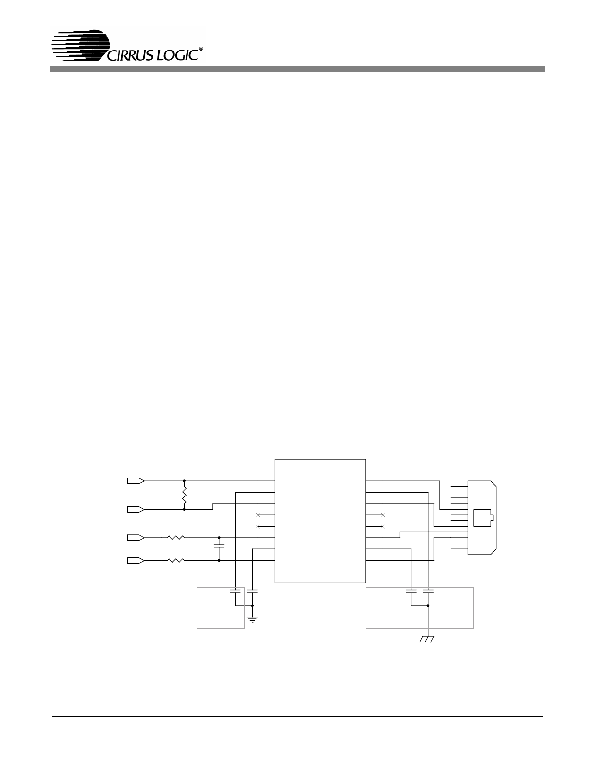
Design Example: CS8900A Interface to Cirrus Logic CL-PS7211
This design is similar to the MC68302 except that
only the I/O mode data access is supported. This
completely elimiates glue logic. See Figure 4. The
highlights of the design are:
- CS8900A I/O space mapped into 7211 memory
- 3 address lines
- A8 and A9 tied high
- AEN used as active low chip select
- SBHE tied to 7211 chip select
- Only 16 bit accesses
Design Example: CS8900A Interface to Hitachi SH3
This design is almost identical to the CL-PS7211
connection diagram. It uses I/O mode only, eliminating glue logic. See Figure 5. The highlights of
the design are:
- CS8900A I/O space mapped into SH3 memory
- 3 address lines - A0 is tied to ground.
- A8 and A9 tied high
- AEN used as active low chip select
- SBHE tied to SH3 chip select
- Inverter on the IRQ line.
- Only 16 bit accesses
Summary
The CS8900A can be interfaced to most non-ISA
system with very minimum or no external logic.
This allows a low cost, small size and very efficient
Ethernet solution for non-ISA systems. Cirrus
Logic will provide support for non-ISA designs,
including logic schematic review and layout review
for design engineers. Those reviews help prevent
logic errors, and help to minimize EMI emissions.
12 AN83REV3
Page 13
AN83
A[3:1]
D[15:0]
nMWE
nMO
nCS
R96
GND
4K99 1%
A[3:1]
A1
A2
A3
D
VD
GND
D[15:0]
D0
D1
D2
D3
D4
D5
D6
D7
D8
D9
D10
D11
D
VD
R97
100K
E
2
D12
D13
D14
D15
nMWE
nMOE
nCS2
CS8900_RST
GND
GND
X3
20M
Hz
93
37
38
39
40
41
42
43
44
45
46
47
48
50
51
52
53
54
58
59
60
65
66
67
68
71
72
73
74
27
26
25
24
21
20
19
18
28
29
62
61
49
36
63
75
77
76
97
98
7
2
RES
SA0
SA1
SA2
SA3
SA4
SA5
SA6
SA7
SA8
SA9
SA10
SA11
SA12
SA13
SA14
SA15
SA16
SA17
SA18
SA19
SD0
SD1
SD2
SD3
SD4
SD5
SD6
SD7
SD8
SD9
SD10
SD11
SD12
SD13
SD14
SD15
CHIPSEL
MEMW
MEMR
IOW
IOR
REFRESH
SBHE
AEN
RESET
SLEEP
TESTSEL
ELCS
XTLI
XTLO
U21
CS8900A
VDD
92256
VCC
VCC
698
VCC
GND
1898694969085
VCCGND
AVSS0
AVSS1
AVSS2
GND
GND
GND
1023555770
AVSS3
AVSS4
GND
GND
VD
AVDD1
AVDD2
D
95
AVDD3
EECS
EESK
EEDATAOUT
EEDATAIN
LED0/HC0
BSTATUS/HC1
LANLED
RXD-
RXD+
TXD-
TXD+
INTRQ0
INTRQ1
INTRQ2
INTRQ3
MEMCS16
IOCS16
IOCHRDY
DMARQ0
DMARQ1
DMARQ2
DMACK0
DMACK2
DMACK3
CSOUT
DO+
DO-
3
4
5
6
D6
LED
99
78
100
84
83
82
CI-
81
CI+
80
DI-
79
DI+
92
91
88
87
32
31
30
35
34
33
64
15
13
11
16
14
12
17
R91
4K7
2 1
2 1
D7
LED
D
VD
ACTIVITY
LINK
R89
390R
R90
390R
R93
100R
R94
8R
R95
8R
EINT
D
VD
VD
D
RxD-
RxD+
TxD-
C62
560pF
TxD+
3
U30A
C94
100nF
1 2
74L
VD
D
C93
100nF
VX04
nURESE
T
VD
D
C89
C91
100nF
C92
100nF
100nF
GND GND GND GND GND GND GND
VDD VDDVDD VDD VDD
C90
100nF
CS8900_RSTnURESET
C88
100nF
Figure 4. CS8900A Interface to Cirrus Logic CL-PS7211
AN83REV3 13
Page 14
3.3V
AN83
SH3 A1
SH3 A2
SH3 A3
SH3 [D15:D0]
SH3 WE1#
SH3 RO#
Chip Select#
3.3V
37
SA0
38
SA1
39
SA2
40
SA3
41
SA4
42
SA5
43
SA6
44
SA7
45
SA8
46
SA9
47
SA10
48
SA11
50
SA12
51
SA13
52
SA14
53
SA15
54
SA16
58
SA17
59
SA18
60
SA19
65
SD0
66
SD1
67
SD2
68
SD3
71
SD4
72
SD5
73
SD6
74
SD7
27
SD8
26
SD9
25
SD10
24
SD11
21
SD12
20
SD13
19
SD14
18
SD15
CS8900A-CQ3
3.3V
0.1uF
9
8
10
DVSS1
DVDD1
DVSS1A
MEMW
MEMR
IOW
28296261496375343364323130351513111614
0.1uF
0.1uF
22
DVDD2
IOR
REFRESH
AEN
23
DVSS2
RESET
56
55
57
DVSS3
DVDD3
DVSS3A
MEMCS16
IOCS16
IOCHRDY
INTRQ0
INTRQ1
INTRQ2
0.1uF
89
INTRQ3
90
AVSS1
DMARQ0
DMARQ1
69
70
DVSS4
DVDD4
RXD-
RXD+
TXD-
TXD+
BSTATUS/HC1
LINKLED/HC0
LANLED
CSOUT
XTAL1
XTAL2
ELCS
CHIPSEL
SBHE
2736
0.1uF
1
DO-
DO+
DI+
CI+
93
AVSS0
DI-
CI-
RES
4.99K
84
83
80
79
82
81
92
91
88
87
78
99
100
17
97
98
510
510
8
8
100
20MHz
LED
LED
RDX-
RXD+
TXD-
560pF
TXD+
3.3V
0.1uF
0.1uF
85
AVDD1
AVDD2
DMARQ2
DMACK0
DMACK1
12
86
DMACK2
77
AVSS2
HWSLEEP
TESTSEL
76
94
AVSS3
EESK
4
95
96
AVSS4
AVDD3
EECS
EEDATAIN
EEDATAOUT
365
RESET
SH3 IRQ0
Figure 5. CS8900A Interface to Hitachi SH3
14 AN83REV3
Page 15

AN83
ETHERNET HARDWARE DESIGN FOR EMBEDDED SYSTEMS AND MOTHERBOARDS
This section describes the hardware design of a
four-layer, 10BASE-T solution intended for use on
PC motherboards, or in other embedded applications. The goal of this design is minimal board
space and minimal material cost. Therefore, a number of features (BootPROM, AUI, 10BASE-2) are
not supported in this particular PCB design. An example of this circuit is included in this technical
reference manual, and is implemented in an ISA
form factor. This same circuit can be implemented
directly on the processor PCB.
General Description
The small footprint, high performance and low cost
of the CS8900A Ethernet solution, makes the
CS8900A an ideal choice for embedded systems
like personal computer (PC) mother boards. The
very high level of integration in the CS8900A results in a very low component count Ethernet design. This makes it possible to have a complete
solution fit in an area of 1.5 square inches.
Board Design Considerations
the CS8900A to interface with variety of microprocessors directly or with the help of simple programmable logic like a PAL or a GAL.
This reference design uses the ISA adapter card
form factor. All the ISA bus connections from the
CS8900A are directly routed to the ISA connector.
The pin-out of the CS8900A is such that if the
CS8900A is placed as shown in Figures 6 and 7,
there will be almost no cross-over of the ISA signals.
External Decode Logic
The CS8900A can be accessed in I/O mode or
memory mode. For this reference design, in memory mode the CS8900A is in the conventional or
upper memory of the PC. That is, it resides in the
lower 1 Mega bytes of address space.
To use the CS8900A in extended memory address
space requires an external address decoder. This
decoder decodes upper 4 bits (LA[20:23]) of 24 bit
ISA address lines. In many embedded microprocessors such decodes are available though the microprocessors itself.
Please refer to “Extended Memory Mode” on
page 31 for further information.
Crystal Oscillator
The CS8900A, in this reference design, uses a
20.000 MHz crystal oscillator. The CS8900A has
internal loading capacitance of 18pF on the
XTAL1 and XTAL2 pins. No external loading capacitors are needed. Please note that the crystal
must be placed very close to XTL1 and XTL2 pins
of the CS8900A.
This crystal oscillator can be eliminated if accurate
clock signal (20.00 MHz ±0.01% and 45-55 duty
cycle) available in the system.
ISA Bus Interface
The CS8900A has a direct ISA bus interface. Note
that the ISA bus interface is simple enough to allow
AN83REV3 15
EEPROM
A 64 word (64 X16 bit) EEPROM (location U3) is
used in the reference design to interface with the
CS8900A. This EEPROM holds the IEEE assigned Ethernet MAC (physical) address for theboard (see “Obtaining IEEE Addresses” on
page 55). The EEPROM also holds other configuration information for the CS8900A. The last few
bytes of the EEPROM are used to store information
about the hardware configuration and software requirements.
In an embedded system, such as a PC, the system
CMOS RAM or any other non-volatile memory
can be used to store the IEEE address and Ethernet
configuration information. In such a case an EE-
Page 16
AN83
CS8900 EVAL REV. B
CRYSTAL SEMICONDUCTOR CORPORATION
CS8900 EVAL BOARD REV. B
P/N CDB8900B
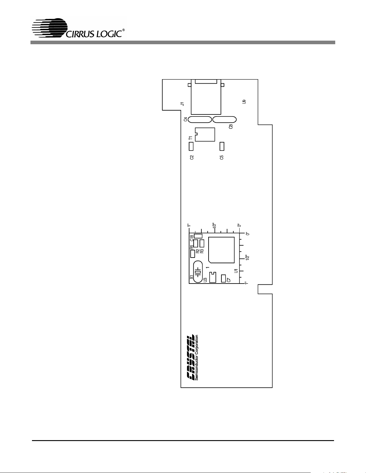
Figure 6. Placement of Components, Top Side
16 AN83REV3
CD B8900B© CO P YR IGH T 1994
Page 17
AN83
CRYSTAL SEMICONDUCTOR CORPORATION
CS8900 EVAL BOARD REV. C
P/N CDB8900B
Figure 7. Placement of Components, Solder Side
AN83REV3 17
Page 18
AN83
PROM is not necessary for the CS8900A, and the
CS8900A will respond to IO addresses 0300h
through 030Fh after a reset.
Please refer to the CS8900A data sheet for information about programming the EEPROM. Please refer to “JUMPERLESS DESIGN” on page 45 of
this document for information about EEPROM internal word assignments.
LEDs
Many embedded systems do not require LEDs for
the Ethernet traffic. Therefore this reference design does not implement any LEDs. However, the
CS8900A has direct drives for the three LEDs.
Please refer to the data sheet for the CS8900A for a
description of the LED functions available on the
CS8900A.
10BASE-T Interface
The 10BASE-T interface for the CS8900A is
straight forward. Please refer to Figure 8 (3.3V)
and Figure 10 (5V) for connections and components of this circuit. Transmit and receive signal
lines from the CS8900A are connected to an isola-
tion transformer at location T1. This isolation
transformer has a 1:1 ratio between the primary and
the secondary windings on the receive side. It has
a 1:√2 (1:1.414) ratio between the primary and the
secondary windings for the transmit lines for 5V
operation or a ratio of 1:2.5 for 3.3V operation. Resistor R1 provides termination for the receive lines.
Resistors R2 and R3 are in series with the differential pair of transmit lines for impedance matching.
10BASE-2 and AUI Interfaces
As many embedded systems require only a
10BASE-T interface, this reference design implements only the 10BASE-T interface. However,
should a user require a 10BASE-2 or AUI interface, the CS8900A provides a direct interface to the
AUI. Please refer to “Low Cost Ethernet Combo
Card Reference Design: CRD8900” on page 21 of
this document for details about the AUI interface.
Logic Schematics
Figures 8, 9 and 10 detail the logic schematics for
the various circuits used in the reference design.
10BT_RD-
10BT_RD+
10BT_TD-
10BT_TD+
8
R4
8
R5
100
R2
560pF
C30
.1uF .1uF
Do Not
Populate
1
1
2
2
(1-3) (16-14) 1:1
3
3
4
4
5
5
6
6
7
(6-8) (11-9) 1:2.5
7
8
8
10BaseT Transformer
C23
16
15
14
13
12
11
10
9
16
15
14
13
12
11
10
9
.1uF 2KV
C29
Do Not
Populate
.1uF 2KV
C28
10
J21
8
7
6
5
4
3
2
1
9
Figure 8. 10BASE-T Schematic 3.3V
18 AN83REV3
Page 19

AN83
SA00
SA01
SA02
SA03
SA04
SA05
SA06
SA07
SA08
SA09
SA10
SA11
SA12
SA13
SA14
SA15
SA16
SA17
SA18
SA19
SMEMW
SMEMR
IOW
IOR
REFRESH
SBHE
AEN
RESET
X1
1
XTAL
20.0 MHz
2
TSTSEL
+5V
4.99k, 1%
R4
93
97
98
37
38
39
40
41
42
43
44
45
46
47
48
50
51
52
53
54
58
59
60
7
28
29
62
61
49
36
63
76
77
75
C12
C14
C13
F
F
ISA_D1
DVDD4
ISA_D2
µ
0.1
DVSS3
ISA_D3
ISA_D4
DVDD3
ISA_D5
F
µ
0.1
ISA_D6
ISA_D7
DVSS2
CS8900
ISA_D8
ISA_D9
µ
0.1
257107069555623228994958685899096164
ELCS
RES
XTL1
XTL2
ISA0
ISA1
ISA2
ISA3
ISA4
ISA5
ISA6
ISA7
ISA8
ISA9
ISA10
ISA11
ISA12
ISA13
ISA14
ISA15
ISA16
ISA17
ISA18
ISA19
CHIPSEL
MEMW
MEMR
IOW
IOR
REFRESH
SBHE
AEN
TESTSEL
SLEEP
RESET
DVSS4
DVSS3A
DVSS1A
ISA_D0
656667687172737427262524212019
DVDD2
U1
C9
F
µ
0.1
ISA_D10
DVSS1
ISA_D11
ISA_D12
ISA_D13
DVDD1
ISA_D14
C8
C11
C10
F
F
µ
0.1
AVSS2
AVDD3
AVDD2
DMACK0
DMACK2
161412
F
µ
0.1
AVSS1
DMACK3
µ
0.1
AVSS3
ISA_D15
18
+5V
AVSS4
AVSS0
AVDD1
EEDATAIN
EECS
EEDATAOUT
LED0/HC0
BSTATUS / HC1
LED2
DO-
DO+
CI+
DI+
RXD-
RXD+
TXD-
TXD+
INTRQ0
INTRQ1
INTRQ2
INTRQ3
MEMCS1 6
I0CS16
I0CH RDY
DMARQ0
DMARQ1
DMARQ2
CSOUT
EE_CLK
EESK
CI-
DI-
3
5
99
78
100
84
83
82
81
80
79
92
91
88
87
32
31
30
35
34
33
64
15
13
11
17
0.1µF
1
CS
2
CLK
3
U3
D1
5
VSS
1K_EEPROM_S
12
C7
8
VCC
4
D0
7
NC2
6
NC1
10BT_RD10BT_RD+
10BT_TD10BT_TD+
IRQ10
IRQ11
IRQ12
IRQ5
MEMCS1 6
I0CS1 6
I0CH RDY
DRQ5
DRQ6
DRQ7
+5V
SD0
SD1
SD2
SD3
SD4
SD5
SD6
SD7
SD8
SD9
SD10
SD11
SD12
SD13
SD14
SD15
DACK5
DACK6
DACK7
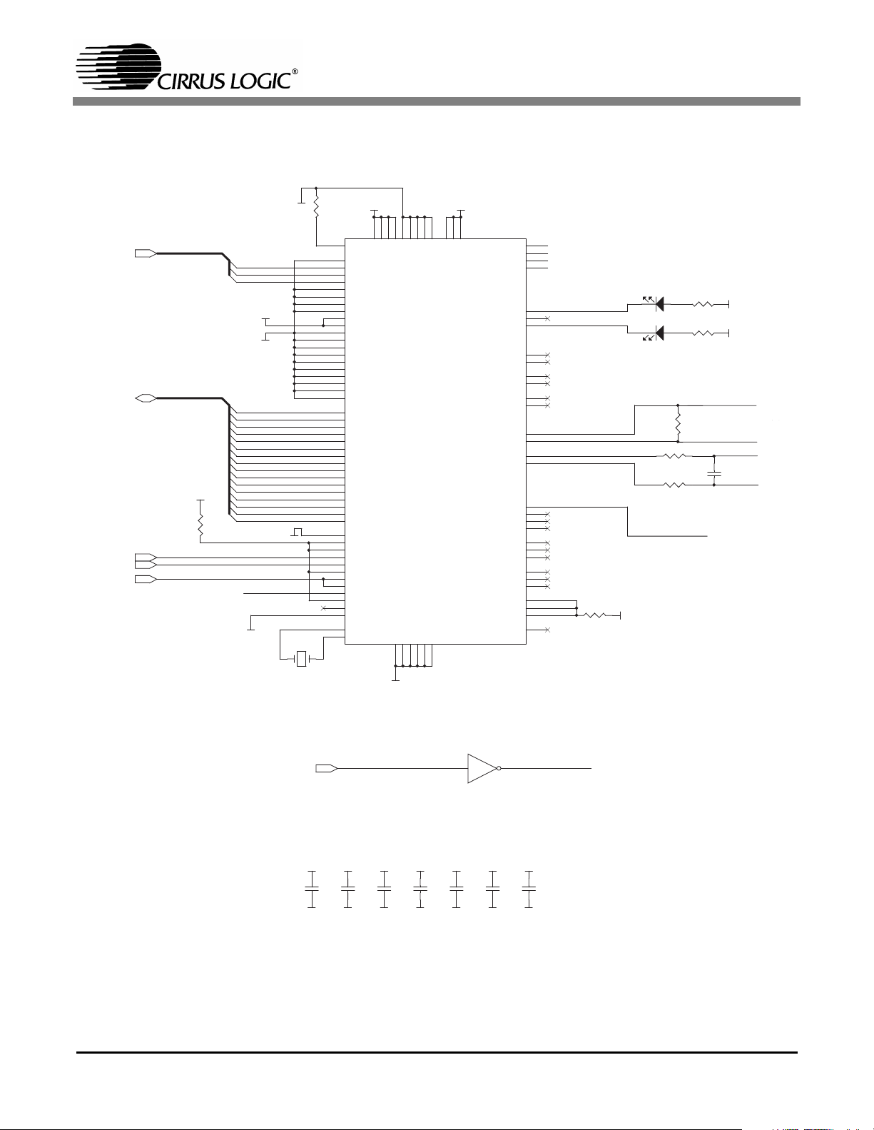
Figure 9. Overall Schematic
AN83REV3 19
Page 20

AN83
.1
C23
1
2
2
3
3
4
4
5
5
6
6
(6-8) (11-9) 1:1.414
7
7
8
8
10 BaseT Transformer
µ
F
10BT_RD-
10BT_RD+
10BT_TD-
10BT_TD+
24.3
R4
24.3
R5
100
R2
68 pF
C30
Do Not
Populate
.1 µF
Figure 10. 10BASE-T Schematic 5V
Component Placement and Signal Routing
Please refer to “Layout Considerations for the
CS8900A” on page 35 of this document for more
details on the placement of components on the
board. It is important to provide very clean and adequate +5 V and ground connections to the
CS8900A.
(1-3) (16-14) 1:1
16
16
15
15
14
14
13
13
12
12
11
11
10
10
9
9
Do Not
Populate
.1 µF 2KV
C29
C17
TANT TANT TANT
+
22µF22µF22µF
.1 µF 2KV
C28
C16 C15
+5V
10
8
J1
7
6
5
4
3
2
1
9
++
Bill of Material
Table 1 has a list components that are typically
used to assemble this adapter card. For most of the
components, there are several alternative manufacturers.
Item Reference # Description Quantity Vendor Part Number
1 C2, C5, C7..C14 Capacitor, 0.1 µF, X7R, SMT0805 10
2 C15, C16, C17 Capacitor, 22 µF, SMT7343 3
3 R2, R3 Resistor, 24.3, 1%, 1/8W, SMT0805 2
4 R1 Resistor, 100, 1%, 1/8W, SMT0805 1
5 R4 Resistor, 4.99K, 1%, SMT0805 1
6* X1 Crystal, 20.000 MHz 1 M-tron ATS-49,20.000 MHz,18 pF
7 J1 Connector, RJ45, 8 pin 1 AMP 555164-1
8 T1 Transformer, 2, 1:1, 1:1.41 1 Valor ST7011 (SOIC)
9 U1 ISA Ethernet Controller 1 Crystal CS8900A
10* U3 1K EEPROM 1 Microchip 93C46 (8 pin SOIC)
Figure 11. Decoupling Capacitors Schematic
* Depending on system resources, these parts may not be needed.
Table 1. CS8900A Design Bill of Materials
GND
20 AN83REV3
Page 21

AN83
LOW COST ETHERNET COMBO CARD REFERENCE DESIGN: CRD8900
This section describes the hardware design of a lowcost, two-layer, full-featured Ethernet solution intended for use in PC ISA-bus. The goal of this design
is a high degree of application flexibility. Therefore,
a number of features (BootPROM, AUI, 10BASE-2)
are supported. An example of this circuit is included
in this Technical Reference Manual.
General Description
The CS8900A ISA Ethernet controller is used in
this low cost, high performance ISA Ethernet
adapter card. This card has AUI, 10BASE-T and
10BASE-2 interfaces. The very high level of integration of the CS8900A results in a very low component count. This makes it possible to design a
half height, two layered 16 bit ISA Ethernet adapter
card. Since the analog filters are integrated on the
CS8900A, the card may be compliant with FCC
part 15 class (B) compliant.
Board Design
A recommended component placement is shown in
Figure 12, and a recommended board schematics
are shown in Figures 10 and 13 through 17.
External Decode Logic
The CS8900A can be accessed in both I/O and
memory modes. The CS8900A internally decodes
the SA[0:19] address lines for the lower 1 M of
memory. The reference design uses an external decode logic to allow the card to also decode decodes
the upper 4 bits of the ISA address (LA[23:20]),
thus allowing the CS8900A to reside anywhere in
extended memory. This decode logic is implemented using a 16R4 PAL at location U4. This logic is
configured by the CS8900A. The PAL then decodes the upper 4 bits of the ISA address. Please refer to “Addressing the CS8900A: I/O Mode,
Memory Mode” on page 27 of this document for
further information.
EEPROM
A 64 word (64 X16) EEPROM (location U3) is
used in the reference design to interface with the
CS8900A. This EEPROM holds the IEEE assigned Ethernet MAC (physical) address for the
board. (see “Embedded Designs” on page 54) The
EEPROM also holds other configuration information for the CS8900A. The last few bytes of the
EEPROM are used to store information about the
hardware configuration and software requirements.
Crystal Oscillator
The CS8900A, in the reference design, uses a
20.000 MHz crystal oscillator. Please note that the
crystal must be placed very close to XTL1 and
XTL2 pins of the CS8900A.
ISA Bus Interface
The ISA bus connections from the CS8900A can be
easily routed to the ISA connector. If the pin-out of
the CS8900A is placed as shown in Figure 12, there
will be almost no cross-over of the ISA signals. It
is also important to provide very clean and adequate +5 V and ground connections to the
CS8900A.
AN83REV3 21
Please refer to the CS8900A datasheet for information about programming the EEPROM. Please refer to “JUMPERLESS DESIGN” on page 45 of
this document for information about EEPROM internal word assignment.
Socket for Optional Boot PROM
A socket is provided at location U6 for the optional
Boot PROM. This Boot PROM is required in systems that require remote boot capability, for example diskless work stations. The 74LS245 data
buffer at U7 is provided for the Boot PROM (See
Figure 15). Inside the CS8900A there are registers
that hold the Boot PROM base address (PacketPage base + 030h) and the Boot PROM address
mask (PacketPage base + 034h). A 20 bit address
Page 22

J4
T B
LED1
AN83
R19
R18
C22 C28
T3
J1
C26
F1
C29
C23
T2
J2
J3
R11
T1
C21
C24
R12
R13
R14
R15
U2
C20
+
C27
R16 R17
D1
U9
R10
CRYSTAL SEMICONDUCTOR CORPORATION
CS8900 COMBO EVAL BOARD REV. B
P/N CDB8900B
CS8900 COMBO EVAL REV. B
C1P
C18
U5
R6
R7
R8
R9
C16
C15
C11 R3 C12 C13
C6 C9
C17
+
C8
U1
C10
C1
+
1
C4 C7
U7
U6
C30
C5
U3
R4R5
R2
X1
C14
C3
U4
C2
U6
CDB8900B©COPYRIGHT 1994
Figure 12. Placement of Components
22 AN83REV3
Page 23

AN83
SA00
SA01
SA02
SA03
SA04
SA05
SA06
SA07
SA08
SA09
SA10
SA11
SA12
SA13
SA14
SA15
SA16
SA17
SA18
SA19
CHIPSEL
MEMW
MEMR
IOW
IOR
REFRESH
SBHE
AEN
RESET
X1
12
XTAL
20.0 MH z
TSTSEL
ELCS
+5V
76
77
75
4.99k
R3
93
97
98
37
38
39
40
41
42
43
44
45
46
47
48
50
51
52
53
54
58
59
60
7
28
29
62
61
49
36
63
ISA_D13
DVDD1
C13
C11
F
µ
0.1
AVSS3
ISA_D14
ISA_D15
18
AVDD3
C12
F
F
µ
µ
0.1
0.1
AVSS2
AVDD2
DMACK0
DMACK2
12
16
14
C16
C17
C8
F
F
µ
µ
0.1
0.1
257107069555623228994958685899096164
RES
XTL1
XTL2
ISA0
ISA1
ISA2
ISA3
ISA4
ISA5
ISA6
ISA7
ISA8
ISA9
ISA10
ISA11
ISA12
ISA13
ISA14
ISA15
ISA16
ISA17
ISA18
ISA19
CHIPSEL
MEMW
MEMR
IOW
IOR
REFRESH
SBHE
AEN
TESTS EL
SLEEP
RESET
ELCS
DVSS 4
DVSS 3
DVDD4
DVSS3A
DVSS1A
ISA_D0
ISA_D1
ISA_D2
ISA_D3
ISA_D4
656667687172737427262524212019
F
µ
0.1
DVDD3
ISA_D5
ISA_D6
ISA_D7
C7
F
µ
0.1
DVSS2
DVSS 1
DVDD2
U1
CS8900
ISA_D8
ISA_D9
ISA_D10
ISA_D11
ISA_D12
+5V
AVSS1
AVSS4
AVDD1
EEDATAOUT
BSTATUS / HC1
DMACK3
EE_CLK
AVSS0
EEDATAI N
EECS
LED0/HC0
LED2
DO-
DO+
CI+
DI+
RXD-
RXD+
TXD-
TXD+
INTRQ0
INTRQ1
INTRQ2
INTRQ3
MEMCS16
I0CS16
I0CHRDY
DMARQ0
DMARQ1
DMARQ2
CSOUT
EE_CLK
EESK
CI-
DI-
3
5
99
78
100
84
83
82
81
80
79
92
91
88
87
32
31
30
35
34
33
64
15
13
11
17
EE_DIN
12
PROM CS
0.1µF
1
CS
2
CLK
3
U3
D1
5
VSS
1K_EEPROM_S
R18
R19
+5V
C5
8
VCC
4
D0
7
NC2
6
NC1
BSTATUS / HC1
LED_T
680
314
LED_B
680
2
DODO+
CICI+
DIDI+
10BT_RD10BT_RD+
10BT_TD10BT_TD+
IRQ10
IRQ11
IRQ12
IRQ5
MEMCS16
I0CS16
I0CHRDY
DRQ5
DRQ6
DRQ7
PROM_CS
SD2
SD3
SD4
SD8
SD0
SD1
SD9
SD5
SD6
SD7
SD13
SD14
SD15
SD10
SD11
SD12
DACK7
DACK 5
DACK6
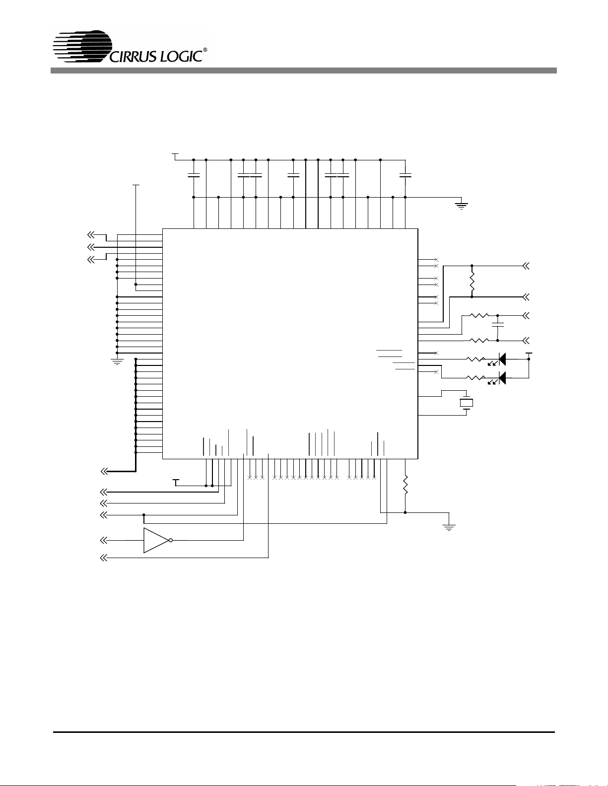
Figure 13. CS8900A Schematic (Combo Card Application)
AN83REV3 23
Page 24

+5V
AN83
PROM_CS
SA00
SA01
SA02
SA03
SA04
SA05
SA06
SA07
SA08
SA09
SA10
SA11
SA12
SA13
SA14
C19
TANT TANT TANT
C10 C1
+
++
22µF22µF22µF
GND
Figure 14. Power Supply Decoupling Schematic
C2
0.1µF
20
CE
22
OE
1
VPP
10
A0
9
A1
A2
A3
A4
A5
A6
A7
A8
A9
A10
A11
A12
A13
A14
U6
27C256
DQ7
DQ6
DQ5
DQ4
DQ3
DQ2
DQ1
DQ0
19
18
17
16
15
13
12
11
8
7
6
5
4
3
25
24
21
23
2
26
27
+5V
PD7 2
PD6 3
PD5 4
PD4 5
PD3 6
PD2 7
PD1 8
PD0 9
4.7k
R1
C4
0.1µF
19
OE
1
DIR
A1
A2
A3
A4
A5
A6
A7
A8
74LS245
U7
B1
B2
B3
B4
B5
B6
B7
B8
18
17
16
15
14
13
12
11
SD7
SD6
SD5
SD4
SD3
SD2
SD1
SD0
Figure 15. Boot PROM Schematic
24 AN83REV3
Page 25

AN83
DO-
DO+
CICI+
DIDI+
BSTATUS/HCI
+12V
R6 39.2
R8
C18
0.1µF
39.2
C14
0.1µF
R7 39.2
CICI+
DIDI+
R9 39.2
Ω
C15
1
+12IN1
2
+12IN2
3
EN
22
U5
EN
23
-12IN1
24
-12IN2
DC-DC
CONVERSION
SOUT+
SOUT-
NC
0.1µF
12
9
13
T2
1
I11
2
I12
4
I21
5
I22
7
I31
8
I32
O11
O12
O21
O22
O31
O32
16
15
13
12
10
9
AUI_XFR_S
Figure 16. AUI Schematic
ISOLATED_GND
C21
0.1µF
-9_V
+12V
CI_A
DO_A
DI_A
CON_AUI15PSUBO
1
2
3
4
5
6
7
8
16 17
C27
C20
0.1µF
F1
J2
0.1µF
VP_+12V
9
CI_B
DO_B
10
11
12
13
14
15
R15 10k R16 121
DI_B
(CS8900 Pin 4)
(CS890 0 Pin2 )
CS890 0 Pin5)
(ISA B28)
(ISA C02)
(ISA C03)
(ISA C04)
(ISA C05)
(ISA B02)
DI+
DI-
CI+
CIDO+
DO-
EE_SK
ELCS
EEDOUT
BALE
LA23
LA22
LA21
LA20
RESET
1082 CI+
1082 CI1082 DI+
1082 DI1082 DO+
1082 DO-
R10 1K
AUI_XFR_S
8
I32
7
I31
5
I22
4
I21
2
I12
1
I11
9
O32
10
O31
12
O22
13
O21
15
O12
16
O11
T1
Figure 17. 10BASE-2 Schematic
11
1
2
3
4
5
6
7
8
9
CLK
G
10
11
12
13
14
15
16
17
PAL16R4
I/00
I/01
I/02
I/03
12
13
18
19
14
00
15
01
16
02
17
03
Figure 18. PAL Decode of LA[20-23]
2
3
4
12
13
14
15
18
19
5
6
7
8
9
10
11
20
21
22
23
24
25
CD+
CDRX+
RX-
TX+
CS83C92C_S
TX-
HBE
RR+
RR-
U2
VEE1
VEE2
VEE3
VEE4
VEE5
VEE6
VEE7
VEE8
VEE9
VEE10
VEE11
VEE12
VEE13
CHIPSEL_B (CS8900 Pin7)
TX0
RX1
CDS
GND1
GND2
NC
D1
BNC_50
1H916
28
TX0
26
RX1
1
CDS
16
17
27
C24
1M
1kV
1/2W
.01µF
R17
J3
1
2
AN83REV3 25
Page 26

AN83
loaded at the Boot PROM base address register indicates the starting location in host memory where
the Boot PROM is mapped. The Boot PROM address mask indicates the size of the Boot PROM.
The lower 12 bits of the mask are ignored and
should be 000h. This limits the 434 Boot PROM
size to increments of 4K bytes. The CS8900A will
not generate an address decode for the Boot PROM
until the Boot PROM base address register and the
mask register are loaded. For example, say a 16K
Boot PROM is used and it is to be located starting
at address 0D0000h. Before this Boot PROM is
accessed, load the following registers with the values shown in Table 2.
Register Word
Offset
PacketPage
Base +
30h 0000h Boot PROM Base address -
32h 000Dh Boot PROM Base address -
34h C000h Boot PROM address mask -
36h 000Fh Boot PROM address mask -
Table 2. BootPROM Descriptions Stored in CS8900A
Hex
value Description
low word
high word
low word
high word
PacketPage
The address mask that will be used by the
CS8900A is 0FC000h. The CS8900A will compare SA[19:14] with the value 0D0h. Whenever
there is a match, it will assert the signal CSOUT
to
generate an address decode for the Boot PROM. In
the reference design, the same signal is also used to
enable the data buffer, 74LS245, at location U7.
LEDs
A pair of LEDs are provided in the reference design
to indicate link OK and line active status. The pair
of LEDs are packaged one on the top of the other at
location LED1. The top LED is driven by the LINKLED pin while the bottom LED is driven by the
LANLED pin of the CS8900A. The top LED lights
up when the CS8900A has the link pulse. The bottom LED lights up when the CS8900A transmits or
receives a packet or senses a collision. The LEDs
are directly driven by the CS8900A. Two 680 Ohm
resistors limit the current flowing through the LED
circuitry.
10BASE-T Interface
The 10BASE-T interface for the CS8900A is
straight forward. Please refer to Figure 8 or 10 for
connections and components of this circuit. Transmit and receive signal lines from the CS8900A are
connected to an isolation transformer at location
T3. For 5V operation this isolation transformer has
a 1:1 ratio between the primary and the secondary
windings on the receive side and 1:√2 (1:1.41) ratio
between the primary and secondary windings for
the transmit lines. For 3.3V operation the receive
side is 1:1 and the transmit side is 1:2.5. Resistor
R2 provides termination for the receive lines. Resistors R4 and R5 are in series with the differential
pair of transmit lines for impedance matching.
AUI Interface
Please refer to Figure 16 for connection of AUI signals to the CS8900A. The AUI lines from the 15pin sub-D connector (location J2) are connected to
the CS8900A through an isolation transformer at
T2. This isolation transformer has three windings
for three pairs of differential AUI signals: transmit,
receive and collision. All three windings have a
turns ratio of 1:1 between the primary and secondary windings. Circuitry consisting of R6, R7 and
C14 provides impedance termination for the collision differential pair. Circuitry consisting of R8,
R9 and C15 provides impedance termination for
the receive differential pair. The +12 volt power
going out to the AUI connector is safeguarded by
the fuse at F1. The AUI interface at J2 can be used
to connect external Media Access Units (MAU).
These MAUs allow the AUI interfaced to be used
to interface with 10BASE-5 or 10BASE-F.
26 AN83REV3
Page 27

AN83
10BASE-2 Interface
A 10BASE-2 transceiver IC, the 83C92C, is used
to generate a 10BASE-2 interface for the reference
design. Please refer to Figure 17 for details about
the components and connection.
A 12 volt to -9 volt DC to DC voltage converter (location U5) is used to generate an isolated -9 volt
supply for the 83C92C. The DC-DC converter
used in the reference design has an enable pin. This
enable pin is connected to the HC1 pin of the
CS8900A. Usually the DC-DC converter is disabled when the 10BASE-2 interface is not used.
This not only reduces power used by the adapter
card but also eliminates any noise the 10BASE-2
circuitry can induce on the 10BASE-T or AUI interface that may be in use. This reference design
uses a “low” enable DC-DC converter. That is, the
DC-DC converter is enabled when the enable pin is
logic low. However, the board can be built with a
“high” enable DC-DC converter. In such a case,
software that controls the enable and disable operations of the DC-DC converter should be modified.
An optional method is to use an integrated module
that includes all the needed 10Base2 components.
Contact Halo Electronics for information on their
TnT integrated 10Base2 modules.
Logic Schematics
ment for an explanation and information about
placement of components on the board.
Bill of Material
Table 3 contains a list of components that are typically used to assemble this adapter card. For most
of the components, there are several alternative
manufacturers.
Addressing the CS8900A: I/O Mode, Memory Mode
The CS8900A, integrated Ethernet controller, has
20 address pins that directly connect to SA[19:0] of
the ISA bus. The CS8900A has an internal address
comparator to compare the ISA address with its
base address registers.
I/O Mode
In IO mode, the lower 16 bits of the ISA address are
compared with the address stored in IO Base Address register (Packet Page base + 020h). When an
address match occurs and one of the IO command
(IOR or IOW) lines is active, the CS8900A responds to that IO access. The lower 4 bits of address lines are ignored by the address comparator.
This dictates that the CS8900A must always be at a
16 byte address boundary of the ISA IO address
space. The pin CHIPSEL
access.
is ignored for an IO mode
Figures 10 and 13 through 17 detail logic schematics for the various circuits used in the reference design.
Component Placement and Routing of Signals
Figure 12 shows the component placement used for
the reference design. Figure 19 shows the routing
of signals on the component side of the printed circuit board (PCB) while Figure 20 shows routing on
the solder side. Please refer to “Layout Considerations for the CS8900A” on page 35 of this docu-
AN83REV3 27
After RESET the CS8900A responds to IO address
0300h. However, this condition can be modified
with use of an EEPROM or by software. Immediately after a reset, the CS8900A reads the EEPROM interfaced to it. If the EEPROM has valid
data (valid start data and correct checksum), it will
read information stored in the EEPROM to initialize its own registers including the IO base address
register. Please refer to the CS8900A datasheet for
details about EEPROM configuration and programming. A CS8900A will always respond to valid IO address (even if its memory mode is enabled).
Page 28

AN83
Figure 19. CRD8900 Top-Side Routing
28 AN83REV3
Page 29

AN83
Figure 20. CRD8900 Bottom Side Routing
AN83REV3 29
Page 30

AN83
Item Reference # Description Quantity Vendor Part Number
Base Configuration: I/O Mode with 10BASE-T Interface
1 C5, C7, C8,
C11..13, C16, C17,
C22, C23, C27
2 C1, C10, C19 Capacitor, 22 µF, SMT7343 3
3 R3 Resistor, 4.99K, 1%, SMT0805 1
4 R18, R19 Resistor, 681, 5%, 1/8W, SMT0805 2
5 X1 Crystal, 20.000MHz,18 pF 1 M-tron ATS-49
6 J4 Board Bracket 1 Globe G436
7 U1 ISA Ethernet Controller 1 Crystal CS8900A
8 U3 1K EEPROM 1 Microchip 93C46
9 R4, R5 Resistor, 24.3, 1%, 1/8W, SMT0805 2
10 R2 Resistor, 100, 1%, 1/8W, SMT0805 1
11 C30 Capacitor, 68 pF, SMT0805 1
12 T3 Transformer, 2, 1:1, 1:1.41 1 Valor ST7010 (SOIC)
13 J1 Connector, RJ45, 8 pin 1 AMP 555164-1
Memory Mode Option
1 C3 Capacitor, 0.1 µF, SMT0805, X7R 1
2 U4 PAL 1 AMD PAL16R4B
Boot PROM Options
1 C2, C4 Capacitor, 0.1 µF, SMT0805, X7R 2
2 R1 Resistor, 4.7K, 5%, 1/8W, SMT0805 1
3 U6 32K X 8 EPROM Socket 1
4 U7 Octal Transceiver 1 TI
AUI Option
1 C14, C15 Capacitor, 0.1 µF, SMT0805, X7R 2
2 R6..R9 Resistor, 39.2, 1%, 1/8W, SMT0805 4
3 F1 Fuse, 1A 1
4 T2 Transformer, 3, 1:1, 100 µH 1 Valor ST7033 (SOIC)
5 J2 Connector, 15-pin sub-D 1 AMP 745782-1
6 J2 AUI Slide Latch 1 AMP 745583-5
10BASE2 Option
1 C18, C20, C21 Capacitor, 0.1 µF, SMT0805, X7R 3
2 C24 Capacitor, 0.01 µF, 1kV 1 NIC Components NCD103M1KVZ5U
3 R11..R14 Resistor, 510, 1%, 1/8W, SMT0805 4
4 R10 Resistor, 1K, 1%, 1/8W, SMT0805 1
5 R17 Resistor, 1M, 10%, 1/2W, TH 1
6 R15 Resistor, 10K, 1%, 1/8W, SMT0805 1
7 R16 Resistor, 121, 1%, 1/8W, SMT0805 1
8 D1 Diode 1 1N916
9 T1 Transformer, 3, 1:1, 100 µH 1 Valor ST7033 (SOIC)
10 U2 Ethernet Coax Transceiver 1 83C92C(PLCC)
11 U5 DC-DC Converter, 12V - 9V 1 Valor PM7215
12 J3 Connector, BNC, 50 Ohm 1 AMP 227161-7
LED Option
1 LED1 Bilevel LEDs 1 Ledtronics 21PCT110T4-G/Y
Capacitor, 0.1 µF, SMT0805, X7R 11
74LS245 (SOIC)
Table 3. CS8900A COMBO Card Reference Design Bill of Materials
30 AN83REV3
Page 31

AN83
Memory Mode
In the memory mode, there are two options where
the CS8900A can be placed in the ISA memory address map, lower memory (below 1 Meg) or extended memory (above 1 Meg). The lower
memory typically consists of the conventional
memory (up to 640K) and upper memory (640K to
1 Meg. boundary). To access anything in extended
memory, the processor (386 and above) is used in
the “Enhanced Mode”.
The CS8900A will respond to IO addresses programmed in its IO Base Address Register (Packet
Page Base + 020h) even if memory mode is enabled. To enable memory mode, first write a proper 20 bit value to Memory Base Address register at
Packet page base + 02Ch & 02Eh. Then set MemoryE (bit 0Ah) in the Bus CTL register (Register
17) to one.
These operations can be performed either by doing
writes using IO mode accesses or using an EEPROM as described in Sections 3.4 and 3.5 of the
CS8900A datasheet. The CS8900A will respond
to an ISA memory access, if the CHIPSEL
active (LOW), and the SA[19:0] match the value
stored in Memory Base Address Registers. The
lower 12 bits of the address lines are always ignored. This dictates that the CS8900A must always
be placed at a 4K boundary in the ISA memory address space.
pin is
Lower Memory Mode
To use a CS8900A in the lower 1 Meg address
space, SMEMRD and SMEMWR lines from the
ISA bus are connected to MEMR and MEMW pins
of CS8900A respectively. The SMEMRD and
SMEMWR signals become active only for the lower 1 Meg of the ISA address space. The CHIPSEL
pin of the CS8900A should be connected to
ground.
Extended Memory Mode
The CS8900A can also be mapped in to the extended memory of a Personal Computer (PC) system.
This provides flexibility and more options when
several components are installed in a PC with
CS8900A based network cards.
To address the CS8900A in extended memory
mode, the processor is used in an enhanced mode.
In an enhanced mode, 24 bits of ISA address lines
are used for address generation. Since the
CS8900A accepts 20 bits of address lines, an external address decoder circuit is required to decode the
4 upper address bits. The CS8900A has interface
pins for external decoder circuit.
This arrangement makes provisions so that the
CS8900A can be placed anywhere in the extended
memory address map as long as it is at a 4K address
boundary. The MEMR
ISA bus are active for any ISA memory space access, therefore, for extended memory mode operation, these signals are connected to the MEMR and
MEMW pins of the CS8900A respectively.
The external address decoder circuit consists of a
single and simple Programmable Array Logic like
a 16R4 or GAL16V8. Please refer to the schematic
shown in Figure 21 as an example of such a decoder circuit. The PAL16R4 has 4 registers Q[23:20].
These registers are programmed by the serial input
via the inputs EESK (clock), ELCS (enable pin)
and EEDataOut (serial data out). This decoder
compares the 4 upper address bits, namely
LA[23:20], with the internal programmable register, Q[23:20]. Before memory mode of the
CS8900A is enabled, Q[23:20] must be initialized
to a proper value.
In the design example, Q[23:20] form a left shift
register. The ELCS pin of the CS8900A is used inconjunction with EESK and EEDataOut pins to
shift in the data for Q[23:20] serially. To program
a value, set the ELSEL bit (bit A in Packet Page
base + 040h) to HIGH. Then the EEPROM inter-
and MEMW signals of the
AN83REV3 31
Page 32

CS8900
AN83
or
Ethernet Interface
AUI or 10 BASE-T
Figure 22. Typical CS8900A Ethernet Connection
face is used to generate the serial data stream on
EEDataOut pin (serial data out) with the EESK (serial clock). Whenever ELSEL bit is set, ELCS pin
becomes active (LOW) instead of EECS pin during
the EEPROM operations. Since the EECS pin remains inactive, the EEPROM that is interfaced to
the CS8900A is not enabled.
For the PAL in the design example, one should use
a “Program disable” EEPROM command. (Opcode
00000b). For example, if the CS8900A is to be
placed at PC memory space of 0A00000h, that
means the Q[23:20] should be 0Ah. To program
the 16R4, write 040Ah at Packet Page Base + 040h.
The instruction will take about 10 micro-seconds to
execute.
The electrical connections required to use external
logic are shown in Figure 21. At reset, the
Resistors
Terminating
Isolation Transformer
Transformer with CMC
Connector
CS8900A samples ELCS pin and if it is not
"LOW", it realizes presence of external address decode logic. The same reset signal also makes
ADD_VALID inactive, and thus prevents a signal
CHIPSEL_b from becoming active until Q[23:20]
are initialized. When a host CPU writes to PacketPage base address + 040h to program values for
Q[23:20], the CS8900A then shifts that data serially in to the PAL or GAL. This makes
ADD_VALID signal active.
From this point onwards LA[23:20] are monitored
whenever ALE is active (HIGH). When the decode
logic finds a match, CHIPSEL_b signal is asserted.
This signal remains asserted until ALE becomes
active and the LA[23:20] do not match with
Q[23:20]. The internal decoder of the CS8900A is
active only when CHIPSEL_b is active (LOW).
(CS8900 Pin 4)
(CS8900 Pin2)
CS890 0 Pin5)
(ISA B28)
(ISA C02)
(ISA C03)
(ISA C04)
(ISA C05)
(ISA B02)
EE_SK
ELCS
EEDOUT
BALE
LA23
LA22
LA21
LA20
RESET
1
CLK
11
G
2
10
3
11
4
12
5
13
6
14
7
15
8
16
9
17
PAL16R4
I/00
I/01
I/02
I/03
12
13
18
19
14
00
15
01
16
02
17
03
CHIPSEL_B (CS8900 Pin7)
Figure 21. PAL Decode of LA[20-23]
32 AN83REV3
Page 33

Figure 23 shows a simple PALASMTM program
for the 16R4 PAL that is used in the design shown
in Figure 21.
;PALASM Design Description
;---------------------------------- Declaration Segment ------------
TITLE High address decoder PATTERN
REVISION
AUTHOR Deva Bodas
COMPANY Crystal Semiconductor
DATE 04/01/1994
CHIP _decoder PAL16R4
AN83
;--------------------------------- PIN Declarations ---------------
PIN 1 SCLK ; Serial clock from the CS8900A pin 4 (EESK)
PIN 2 CS_EL_b ; External Logic enable from the CS8900A pin 2 (ELCS*)
PIN 3 SDATA ; Serial data in from the CS8900A pin 5 (EEDataOut)
PIN 4 ALE ; Address latch enable from the ISA bus
PIN 5 LA23 ; Address 23
PIN 6 LA22 ; Address 22
PIN 7 LA21 ; Address 21
PIN 8 LA20 ; Address 20
PIN 9 RESET ; ISA reset pin
PIN 11 OE ; Output enable for the registered outputs
PIN 12 ADD_VALID COMB ; When high, Q[23:20] are programmed
PIN 13 EQUALH COMB ; Upper 2 bits of address match
PIN 19 EQUALL COMB ; Lower 2 bits of address match
PIN 18 CHIPSEL_b COMB ; CHIPSEL
PIN 14 Q20 ; REG
PIN 15 Q21 ; REG
PIN 16 Q22 ; REG
PIN 17 Q23 ; REG
;----------------------------------- Boolean Equation Segment ------
EQUATIONS
to the CS8900A pin 7
; Serial shift register
; When CS_EL_b is inactive (1), no change
; When CS_EL_b is active (0), shift in data
AN83REV3 33
Page 34

Q20 := (Q20 * CS_EL_b) + (/CS_EL_b * SDATA)
Q21 := (Q21 * CS_EL_b) + (/CS_EL_b * Q20)
Q22 := (Q22 * CS_EL_b) + (/CS_EL_b * Q21)
Q23 := (Q23 * CS_EL_b) + (/CS_EL_b * Q22)
; Decode logic
EQUALL = (Q20:*:LA20) * (Q21:*:LA21) ; :*: -> Exclusive NOR operator
EQUALH = (Q22:*:LA22) * (Q23:*:LA23)
ADD_VALID = /RESET * CS_EL_b * ADD_VALID ; stay clear till any write
+ /RESET * /CS_EL_b ; Set when address write
+ /RESET * ADD_VALID ; Remain set until reset
CHIPSEL_b = RESET ; Get set at RESET
+ /ADD_VALID ; Remain set till address is valid
+ (/ALE * CHIPSEL_b ; Do not change when ALE is LOW
+ (ALE * /(EQUALL * EQUALH)) ; Clear during ALE if address matches
AN83
; When ALE is active; CS_b goes active if EQUAL[1:2] are true
; When ALE is inactive; previous state of CS_b is latched.
Figure 23. PAL Program
34 AN83REV3
Page 35

AN83
Layout Considerations for the CS8900A
The CS8900A is a mixed signal device having digital and analog circuits for an Ethernet communication. While doing the PCB layout and signal
connections, it is important to take the following
precautions:
- Provide a low inductive path to reduce power
and ground connection noise.
- Provide proper impedance matching especially
to the Ethernet analog signals.
- Provide low inductive path, wider and short
traces, for all analog signals.
It is important that a PCB designer follow suggestions made in this document for proper and reliable
operation of the CS8900A. These guidelines will
also benefit the design with good EMI test results.
General Guidelines
Figure 24 shows component placement for an ISA
COMBO Ethernet adapter card using a CS8900A.
The placement of the CS8900A should be such that
the routes of the analog signals and the digital signals are not intermixing. No signal should route
beneath the CS8900A on any plane.
Power Supply Connections
The CS8900A has 3 analog and 4 digital power pin
pairs (Vcc and GND). Additional ground connections are provided. Each power pin pair should be
connected to a 0.1 µF bypass capacitor. Connect
the extra ground pins directly the ground plane.
Two Layered Printed Circuit Board (PCB)
A two layered PCB has signal traces on the component and solder side of the PCB. Fill unused areas
with copper planes. Typically, planes on the component side of the PCB are connected to ground
and those on the solder side are connected to VCC
or +5 volts.
Provide each pair of power pin with a 0.1 µF bypass
capacitor. Place each bypass capacitor as close as
possible to the corresponding power pin pair. Con-
nect the capacitor to the pads of the power pins by
short, wide traces, the other end of these traces
should be connected to VCC and GND planes. Figure 19 and Figure 20 illustrate ground and power
(Vcc) plane connections, respectively.
Multi-layered Printed Circuit Board
A multi-layered printed circuit board (PCB) typically has separate ground and power (Vcc) planes.
Multi-layered PCBs are required when the component and trace density is high. Often discrete components like resistors and capacitors are placed on
the solder side of a printed circuit board.
For a multi-layer PCB with all components on one
side of the board, follow the power connection
guide lines as explained in “Two Layered Printed
Circuit Board (PCB)” on page 35. Instead of con-
necting the ground and Vcc to the copper fills on
the component and solder side of the board, connect them to the internal ground and Vcc planes.
Figures 27 through 30 show the four layers of the
four-layer card.
For a multi-layered board the discrete components
are to be placed on the solder side of the PCB, bypass capacitors for the CS8900A can be placed on
the solder side of the PCB. Each bypass capacitor
should be placed beneath the CS8900A and closest
to its corresponding power pin pair. Figures 31
and 32 illustrate the placement and routing of one
bypass capacitor.
Routing of the Digital Signals
Most of the digital signals from the CS8900A go to
the ISA bus connector. Route these signals directly
to the connector. Isolate the digital signals from
analog signals.
Routing of the Analog Signals
Routing of the clock signals: Place the
20.000 MHz crystal within one inch of XTL1 (pin
#97) and XTL2 (pin #98) pins of the CS8900A.
AN83REV3 35
Page 36

J4
T B
LED1
AN83
R19
R18
C22 C28
T3
J1
C26
F1
C29
C23
T2
J2
J3
R11
T1
C21
C24
R12
R13
R14
R15
U2
C20
+
C1P
C27
R16 R17
D1
U9
R10
CRYSTAL SEMICONDUCTOR CORPORATION
CS8900 COMBO EVAL BOARD REV. B
P/N CDB8900B
CS8900 COMBO EVAL REV. B
C18
U5
R6
R7
R8
R9
C16
C15
C11 R3 C12 C13
C6 C9
C17
+
C8
U1
C10
C1
+
1
C4 C7
U7
U6
C30
C5
U3
R4R5
R2
X1
C14
C3
U4
C2
U6
CDB8900B©COPYRIGHT 1994
Figure 24. General placement on an ISA adapter card
36 AN83REV3
Page 37

AN83
CS8900 EVAL REV. B
CRYSTAL SEMICONDUCTOR CORPORATION
CS8900 EVAL BOARD REV. B
P/N CDB8900B
Figure 25. Placement of Components, Top Side
AN83REV3 37
CD B8900B©CO PYRIGH T 1994
Page 38

AN83
CRYSTAL SEMICONDUCTOR CORPORATION
CS8900 EVAL BOARD REV. C
P/N CDB8900B
Figure 26. Placement of Components, Solder Side
38 AN83REV3
Page 39

AN83
Figure 27. Component (top) side of four-layer board
Figure 2.4.6. Component (top) side of four-layer board
AN83REV3 39
Page 40

AN83
Figure 2.4.7. +5V Plane of four-layer board
Figure 28. +5V Plane of four-layer board
40 AN83REV3
Page 41

AN83
Figure 29. Ground Plane of four-layer board
Figure 2.4.8. Ground Plane of four-layer board
AN83REV3 41
Page 42

AN83
Figure 30. Solder side (bottom) of four-layer board
Figure 2.4.9. Solder side (bottom) of four-layer board
42 AN83REV3
Page 43

Figure 31. Placement of Decoupling Capacitor (Bottom side, under CS8900A)
AN83
Figure 32. Routing of Decoupling Capacitor (Top side, component side)
The 20.000 MHz crystal traces should be short,
have no via, and run on the component side.
Biasing resistor at RES pin of the CS8900A: A
4.99 KΩ resistor is connected between pins RES
(pin #93) and AVSS3 (pin #94) of the CS8900A.
This resistor biases internal analog circuits of the
CS8900A, and should be placed as close as possible to RES pin (pin #93) of the CS8900A.
ferential transmit signals and two differential receive signals. An isolation transformer is placed
between the transmit and receive traces and a RJ-45
(modular phone jack) connector. The isolation
transformer should be placed as close as possible to
the RJ-45 connector. Both transmit and receive
signal traces should be routed so they are parallel
and of equal length. The signal traces should be on
the component side and should have direct and
Routing of the 10BASE-T signals: Four signals
are used for 10BASE-T communication, two dif-
AN83REV3 43
short paths. The widths of the receive signal traces
should at least be 25 mil. while widths of the trans-
Page 44

mit signal traces should be at least 100 mil. This
will provide a good impedance matching for the
transmit and receive circuitry inside the CS8900A.
A ground trace should be run parallel to the transmit traces. Also, a ground plane should run underneath the transmit and receive traces on the solder
side of a two layered PCB. Please refer to the Figures 33 and 34 for illustration of the above guide
lines.
Routing of the AUI signals: The CS8900A has
three pairs of differential signals connecting it to an
Auxiliary Unit Interface (AUI). An isolation transformer separates the three signal pairs and the AUI
connector (a 15 pin sub-D connector). The isolation transformer should be placed as close as possible to the AUI connector. Signal traces of each
differential pair should be in parallel with equal
length and impedance. Thus minimizing differential noise due to impedance mismatch. Place the
AUI signal traces on the component side.
AN83
RECOMMENDED MAGNETICS FOR THE CS8900A
The CS8900A is has two types of Ethernet interfaces 10BASE-T and AUI. For both the interfaces,
analog filters are on the chip. The Figures 10 and
16 show typical connection required for these interfaces.
For an AUI interface, an isolation transformer
without a common mode choke (CMC) is used.
For the 10BASE-T interface, choice between isolation transformer and isolation transformer with a
common mode choke (CMC) depends on the common mode noise that exists on the 10BASE-T lines
in a particular system. A common mode choke reduces common mode noise emitted by the
10BASE-T lines. A CMC may be required in certain applications to meet EMI requirements and to
meet 10BASE-T common mode output voltage
noise specification. The physical dimensions of the
isolation transformer and the isolation transformer
with a CMC are the same. Both are typically avail-
Figure 33. 10BASE-T Transit Layout Details
44 AN83REV3
Page 45

AN83
Figure 34. 10BASE-T Receive Layout Details
able in a 16 pin DIP or 16 pin SOIC package. See
tables 4 and 5 for recommended part numbers.
JUMPERLESS DESIGN
Using the CS8900A, both add-in adapters and
motherboard solutions can be implemented without
hardware jumpers or switches. The CS8900A and
media access control (MAC) device drivers obtain
configuration information directly from nonvolatile memory. For add-in ISA adapters, a serial EEPROM will be connected directly to the CS8900A
via the serial interface. Motherboard solutions
may use an on-board serial EEPROM or other nonvolatile memory such as a flash EPROM-based
BIOS. Typically, a separate software utility is used
to initially store and modify the configuration information.
Serial EEPROM
Two types of configuration information is stored in
the EEPROM: configuration information automatically loaded into the CS8900A after each reset and
driver configuration information used by the MAC
driver.
Reset Configuration Block
After each reset (except EEPROM reset) the
CS8900A checks to see if an EEPROM is connected. If an EEPROM is present, the CS8900A automatically loads the first block of data stored in the
EEPROM into its internal registers. This block of
data is referred to as the Reset Configuration
Block. It is used to initialize the CS8900A after
each reset.
Software resets may occur frequently and performance will be enhanced if chip re-initialization
takes as little time as possible. Therefore, since EEPROM readout takes approximately 25 µsec. per
word, the length of the Reset Configuration Block
should be kept to a minimum.
The MAC drivers provided by Cirrus will retain
AN83REV3 45
much of the adapter’s configuration across soft-
Page 46

AN83
Vendor name Description Through-hole Surface-mount
Halo Electronics Isolation transformer, 100 µH TD01-1006K TG01-1006N
Pulse Engineering Isolation transformer, 100 µH PE-64503 PE-65728
Valor Electronics Isolation transformer, 100 µH LT6033 ST7033
Table 4. Partial List of Recommended AUI Transformers
Vendor name Description Through-hole Surface-mount
Halo Electronics Transformer 1:1::1:1.41 TD42-2006Q TG42-1406N1
Transformer with CMC TD43-2006K TG43-1406N
Industrial temperature 1:1::1:1.41 TG42-2006N1
Industrial temperature 1:1::1:1.41
with CMC
3.3V Commercial/Industrial
temperature 1:1::1:2.5
3.3V Commercial/Industrial
temperature with CMC
For PCMCIA versions contact Halo
Pulse Engineering Isolation transformer 1:1::1:1.41 PE-65994 PE-65745
Transformer with CMC PE-65998 PE-65746
3.3V Transformer 1:1::1:2.5
with CMC
3.3V Industrial temperature 1:1::1:2.5
with CMC
Valor Electronics Isolation transformer 1:1::1:1.41 PT4069 ST7011
Transformer with CMC PT4068 ST7010
TG43-2006N
TG92-2006N1
TG41-2006N
E2023
EX2024
Table 5. Partial list of Recommended 10BASE-T Transformers
Company and Address Telephone FAX
Halo Electronics, Inc.
Redwood City, CA 94063
http://www.haloelectronics.com
Pulse Engineering
PO Box 12235
San Diego, CA 92112
http://www.pulseeng.com
Valor Electronics (merged with Pulse)
9715 Business Park Avenue,
San Diego, CA 92131
http://www.pulseeng.com
Table 6. Transformer Vendors
(415)-568-5800 (415)-568-6161
(858)-674-8100 (858)-674-8262
(858)-537-2500 (858)-537-2525
ware resets. Therefore, the only information required in the Reset Configuration Block when used
with Cirrus-provided drivers will be the IO base address (if different than the default 300h) and Boot
PROM configuration when a Boot PROM is used.
Table 7 shows an example of a typical Reset Configuration Block for an adapter with a Boot PROM.
The first word of the block indicates the type of EEPROM in use and the length of the Reset Configuration Block (the number of bytes loaded into the
CS8900A after reset). The last word of the block
contains an 8-bit checksum (in the high byte) of all
the bytes in the block. Refer to the CS8900A Data
46 AN83REV3
Page 47

AN83
Sheet for additional information on the operation of
the EEPROM.
Addr Word Description
00h A110h Sequential EEPROM, 16 bytes follow
01h 0020h 1 word into PP_020 (IO Base Addr)
02h 0210h IO Base Address = 210h
03h 3030h 4 words beginning at PP_030
04h 8000h Boot PROM base at C8000h
05h 000Ch
06h C000h Boot PROM mask of FC000h (16K)
07h 000Fh
08h 1600h Checksum
Table 7. EEPROM Reset Configuration Block
Driver Configuration Information
The CS8900A supports random access to 16-bit
words in the EEPROM through software control.
Therefore, in addition to the configuration data
stored in the Reset Configuration Block automatically loaded by the CS8900A after each reset, addi-
tional configuration information can be stored in
the EEPROM and accessed by the MAC driver.
Typically, this additional configuration information includes the unique IEEE physical address for
the adapter. It may also contain device configuration information used by the MAC driver such as
hardware version, media capabilities, and bus configuration (IRQ, DMA, and memory).
Format of Driver Configuration Block
Table 8 defines the format of the block of configuration information (referred to as the Driver Configuration Block) required for use with MAC
drivers provided by Cirrus. Cirrus recommends all
fields be initialized to their default values before
shipping the adapter. Default values for each field
are indicated in the following sections. All reserved fields should be set to zero.
Note: The Driver Configuration Block must start at
EEPROM word address 1Ch to ensure compatibility with MAC drivers supplied by Cirrus.
Addr. Description Bit(s) Function
1Ch IA bits[39-32], bits[47-40] 15-0 IEEE individual node address
1Dh IA bits[ 23-16], bits[31-24] 15-0 IEEE individual node address
1Eh IA bits[ 7-0], bits[15-8] 15-0 IEEE individual node address
1Fh ISA Configuration Flags
Memory Mode Flag 15 0 = memory mode disabled, 1 = memory mode enabled
Boot PROM Flag 14 0 = no Boot PROM, 1= Boot PROM installed
StreamTransfer 13 0 = disabled, 1 = enabled
DMA Burst 12 0 = disabled, 1 = enabled
RxDMA Only 11 0 = disabled, 1 = enabled
Auto RxDMA 10 0 = disabled, 1 = enabled
DMA Buffer Size 9 0 = 16K, 1 = 64K
IOCHRDY Enable 8 0 = disabled, 1 = enabled
Use SA 7 0 = disabled, 1 = enabled
DMA Channel 6-4 0 = DRQ5, 1 = DRQ6, 2 = DRQ7, 3 = DMA Disable
IRQ 3-0 0 = IRQ10, 1 = IRQ11, 2 = IRQ12, 3 = IRQ5
20h PacketPage Mem Base 15-4 12 MSBs of 24-bit address (lower 12 bits assumed = 0)
Reserved 3-0 Reserved for future use, set to 0
21h Boot PROM Base 15-4 12 MSBs of 24-bit address (lower 12 bits assumed = 0)
Reserved 3-0 Reserved for future use, set to 0
22h Boot PROM Mask 15-4 12 MSBs of 24-bit addr mask (lower 12 bits assumed = 0)
Reserved 3-0 Reserved for future use, set to 0
Table 8. EEPROM Driver Configuration Block
AN83REV3 47
Page 48

Addr. Description Bit(s) Function
23h Transmission Control
HDX/FDX 15 0 = Half-Duplex, 1 = Full-Duplex
Reserved 14-7 Reserved for future use, set to 0
Ignore Missing Media 6 0 = Media required for driver to load, 1 = media not required
Reserved 5-0 Reserved for future use, set to 0
24h Adapter Configuration
Ext. 10B-2 Cable Circuitry 15 0 = Not Present, 1 = Present
LoRx Squelch 14 0 = LoRx Squelch disabled, 1 = LoRx Squelch enabled
PolarityDis 13 0 = polarity correction enabled, 1 = pol. correction disabled
24h Adapter Configuration (Continued)
Optimization Flags 12-11 00 = Server, 01 = DOS Client, 10 = Multi-OS Client
Reserved 10-8 Reserved for future use, set to 0
DC/DC Converter Polarity 7 0 = Low enable, 1 = High enable
Media Type in Use 6-5
LA Decode Circuitry 4 0 = Not Present, 1 = Present (Req’d for decode above 1MB)
HW Standby 3 0 = HW Standby not supported, 1 = HW Standby supported
10BASE-2 Circuitry
AUI Circuitry 1 0 = Not Present, 1 = Present
10BASE-T Circuitry
25h EEPROM Revision 15-0 Revision number of the EEPROM format definition used
26h Reserved 15-0 Reserved for future use, set to 0
27h Mfg Date
Year 15-9 e.g. 1011111b = 1995, 0000001b = 2001
Month 8-5 e.g. 1b = Jan, 1100b = Dec
Day 4-0 e. g . 1b = 1, 11111b = 3 1
28-2Ah IEEE Individual Addr 47-0 Copy of words at 1C-1Eh
2Bh Reserved 15-0 Reserved for future use, set to 0
2Ch Reserved 15-0 Reserved for future use, set to 0
2Dh Reserved 15-0 Reserved for future use, set to 0
2Eh Reserved 15-0 Reserved for future use, set to 0
2Fh Checksum 15-0 Word-wide checksum of words 1Ch to 2Fh (zero sum)
30h EISA ID (low word) 15-0 EISA ID bits[7-0], EISA ID bits[15-8]
31h EISA ID (high word) 15-0 EISA ID bits[23-16], EISA ID bits[31-24]
32h Serial No (low word) 15-0 32-bit OEM assigned serial number, bits[15-8], bits[7-0]
33h Serial No (high word) 15-0 32-bit OEM assigned serial number, bits[31-24], bits[23-16]
34h Serial ID Checksum
Marker Byte 15-8 Constant 0Ah in high byte of checksum word
LFSR Checksum 7-0 8-bit LFSR checksum of words 30h to 33h
Table 8. EEPROM Driver Configuration Block
0 = Auto Detect, 1 = 10BASE-T, 2 = AUI, 3 = 10BASE-2
2 0 = Not Present, 1 = Present
0 0 = Not Present, 1 = Present
AN83
48 AN83REV3
Page 49

AN83
IEEE Physical Address
The format of the 48-bit IEEE physical address as expected by the MAC driver is illustrated by the following example. (Must be initialized by OEM before shipping adapter.)
Example physical address: 000102030405h
Addr Word Description
1Ch 0100h 2 MSB of address (byte reversed)
1Dh 0302h Middle 2 bytes (byte reversed)
1Eh 0504h 2 LSB of address (byte reversed)
ISA Configuration Flags
The ISA Configuration Flags specify how the CS8900A will utilize ISA system resources.
Bit 15 Memory Mode Flag - Indicates the CS8900A will use shared memory for IO operations.
Refer to the CS8900A Data Sheet for a description of the shared memory interface. Default
is disabled.
Bit 14 Boot PROM Flag - Indicates a Boot PROM is installed. Refer to the CS8900A Data Sheet
for discussion of Boot PROM. (Must be initialized by OEM before shipping adapter.)
Bit 13 StreamTransfer Mode - Refer to the CS8900A Data Sheet for description of SteamTransfer
mode. Default is disabled.
Bit 12 DMA Burst - Refer to BusCTL Register of the CS8900A Data Sheet for a discussion of
DMA Burst control. Default is enabled.
Bit 11 RxDMA Only - Refer to the CS8900A Data Sheet for a description of RxDMA Only mode.
Default is disabled.
Bit 10 Auto RxDMA - Refer to the CS8900A Data Sheet for a description of Auto RxDMA mode.
Default is disabled.
Bit 9 DMA Buffer Size - Refer to the CS8900A Data Sheet for a discussion of DMA Buffer size.
Default is 16K.
Bit 8 IOCHRDY Enable - Refer to the BusCTL Register, of the CS8900A Data Sheet for a dis-
cussion of IOCHRDY control. Default is enabled.
Bit 7 UseSA - Refer to the BusCTL Register, of the CS8900A Data Sheet for a discussion of Us-
eSA control. Default is enabled.
Bits 6-4 DMA Channel Select - Refer to the CS8900A Data Sheet for a discussion of DMA channel
selection for the CS8900A. Default is disabled.
Bits 3-0 IRQ Channel Select - Refer to the CS8900A Data Sheet for the typical ISA Bus, CS8900A
pin to pin connection. Cirrus’ pre-written drivers expect the pins to be connected as described in the datasheet when running in an x86 system.
AN83REV3 49
Page 50

AN83
PacketPage Memory Base
Bits 15-4 12 MSB of Memory Base Address - The twelve most significant bits of the 24-bit address
locating the base of the CS8900A’s PacketPage memory. The lower twelve bits are assumed to be 0. Default is 0.
Bits 3-0 Reserved (set to 0)
Boot PROM Memory Base
Bits 15-4 12 MSB of Memory Base Address - The twelve most significant bits of the 24-bit address
locating the base of the CS8900A’s PacketPage memory. The lower twelve bits are assumed to be 0. Default is 0.
Bits 3-0 Reserved (set to 0)
Boot PROM Mask
Bits 15-4 12 MSB of Boot PROM Addr. Mask - Twelve-bit Boot PROM address mask. The lower
twelve bits are assumed to be 0. Refer to the CS8900A Data Sheet for a discussion of the
Boot PROM mask. Default is 0.
Bits 3-0 Reserved (set to 0)
Transmission Control
Bit 15 Full Duplex Mode - Specifies full-duplex or half-duplex mode for transmission. Default is
0 (half-duplex operation).
Bits 14-7 Reserved (set to 0)
Bit 6 Ignore Missing Media (IMM) - Specifies device driver’s behavior if a cable or AUI is not
connected during driver initialization. The driver’s behavior can be summarized by the following four cases. Default is 0.
CASE 1 (IMM = 0, media autodetect selected, cable not connected)
Driver disables TX/RX and unloads if dynamic load/unload is supported by OS.
CASE 2 (IMM = 0, media type specified
[10B-T,AUI,10B-2], cable not connected)
Driver disables TX/RX and unloads if dynamic load/unload is supported by OS.
CASE 3 (IMM = 1, media autodetect selected, cable not connected)
Driver disables TX/RX and unloads if dynamic load/unload is supported by OS.
CASE 4 (IMM = 1, media type specified
[10B-T,AUI,10B-2], cable not connected)
Driver remains resident, reports "Media type XXXXX not detected", and functions normally if/when the specified cable type is connected.
Bits 5-0 Reserved (set to 0)
50 AN83REV3
Page 51

Adapter Configuration Word
Bits 15-13 Reserved (set to 0)
Bits 12-11 Optimization Flags
Used to specify the platform’s OS configuration to the driver. Each driver configures the
CS8900A for optimum performance based on the platform’s OS and driver architecture
(NDIS 2X, ODI, NDIS 3X, etc.). Default is DOS (single threaded OS).
Bits 10-8 Reserved (set to 0)
Bit 7 DC to DC Converter Polarity
Refer to “10BASE-2 Interface” on page 27. (Must be initialized by OEM before shipping
adapter.)
Bit 6-5 Media Type In Use
Specifies the type of media the driver should use (10BASE-T, AUI, 10BASE-2) or if driver
should auto-detect media in use. Default is auto-detect.
Bit 4 Adapter Provides LA Decode Circuitry
Specifies the presence of LA decode circuitry on the adapter. Refer to “Extended Memory
Mode” on page 31. (Must be initialized by OEM before shipping adapter.)
AN83
Bit 3 Adapter Provides HW Standby Circuitry
Specifies the presence of hardware standby circuitry on the adapter. Refer to the CS8900A
Data Sheet. (Must be initialized by OEM before shipping adapter.)
Bit 2 Adapter Provides 10BASE-2 Circuitry
Specifies the presence of 10BASE-2 circuitry on the adapter. (Must be initialized by OEM
before shipping adapter.)
Bit 1 Adapter Provides AUI Circuitry
Specifies the presence of AUI circuitry on the adapter. (Must be initialized by OEM before shipping adapter.)
Bit 0 Adapter Provides 10BASE-T Circuitry
Specifies the presence of 10BASE-T circuitry on the adapter. (Must be initialized by OEM
before shipping adapter.)
EEPROM Revision
Specifies the revision level of the format definition used by this EEPROM. A value of 0 indicates the first
revision level, a value of 1 indicates the second revision level, and so on.
AN83REV3 51
Page 52

AN83
Manufacturing Date
This word is the adapter’s manufacture date encoded in 16 bits, YR-MO-DY format. (Must be initialized
by OEM before shipping adapter.)
Bits 15-9 Two Least-significant Digits of Year
Seven bits for a range of 00 to 99 decimal. A roll-over to 00 will be interpreted as the year
2000.
Bits 8-5 Month
Four bits for a range of 01 to 12.
Bits 4-0 Day
Five bits for a range of 01 to 31.
IEEE Physical Address (Copy)
This field is a copy of the three words at address 1Ch to 1Eh. (Must be initialized by OEM before shipping
adapter.)
16-bit Checksum
The checksum stored at the end of the block is the 2’s complement of the 16-bit sum of all the preceding
words in the Driver Configuration Block. (The drivers access the Configuration Block as 16-bit words.)
Any carry out of the 16th bit is ignored. Since this checksum value is calculated as the 2’s complement of
the sum of all the preceding words in the block, a total of 0 should result when the checksum value is added
to the sum of the previous words. (Must be initialized by OEM before shipping adapter.)
EISA ID
The two EISA words make up the 32-bit EISA Product Identification Code.
Low Word These 16 bits make up the 3-letter identifier string of the OEM’s EISA ID in 5-bit com-
pressed ASCII. (A = 00001, B = 00010, C = 00011, etc.)
Bits 7-0 High order 8 bits of 16-bit value
Bits 15-8 Low order 8 bits of 16-bit value
High Word These 16 bits make up the OEM’s product ID No.
The upper order 11 bits are the product ID number and the lower order 5 bits are the revision
number.
Bits 7-0 High order 8 bits of 16-bit value
Bits 15-8 Low order 8 bits of 16-bit value
52 AN83REV3
Page 53

AN83
Serial Number
The two serial number words make up the unique 32-bit OEM serial number for the adapter.
Low Word
Bits 7-0 bits[7-0] of 32-bit serial number
Bits 15-8 bits[15-8] of 32-bit serial number
High Word
Bits 7-0 bits[31-24] of 32-bit serial number
Bits 15-8 bits[23-16] of 32-bit serial number
Serial ID Checksum
Word 34h contains an 8-bit LFSR checksum calculated on the EISA ID and OEM serial number (words
30h to 33h). The 8-bit LFSR checksum is placed in the low byte of 34h. The high byte is padded with
the constant 0Ah.
AN83REV3 53
Page 54

AN83
Maintaining EEPROM Information
The contents of the EEPROM may either be preprogrammed in a stand-alone EEPROM programmer or programmed after installation through the
CS8900A’s serial interface. See the CS8900A
Data Sheet for programming an EEPROM via the
CS8900A’s serial interface. The OEM is left to determine the best procedure for programming EEPROMs via a stand-alone EEPROM programmer.
Cirrus has two utilities suitable for maintaining the
configuration information stored in the EEPROM.
IAGEN.EXE generates a file with individual addresses and serial numbers. EEPROM.EXE is designed to be used by OEMs to initialize the
EEPROM’s contents before shipping to the end-user. It takes the file generated by IAGEN.EXE as input. Both utilities are available as executables and
source code on request.
Cirrus also provides SETUP.EXE, a DOS-based
Setup and Installation Utility run by the end-user at
the time the adapter is installed. The DOS-based
Setup and Installation utility allows the end-user to
configure the adapter for a specific system.
Embedded Designs
Embedded designs may be implemented using an
on-board serial EEPROM connected to the
CS8900A in the same manner as is used in adapter
board designs. However, to save board space and
reduce costs, motherboard implementations can
store the Driver Configuration Block in the system’s BIOS nonvolatile memory.
BIOS-Based Design Considerations
For Cirrus supplied MAC drivers to interface with
a Driver Configuration Block (DCB) stored in
BIOS, the DCB’s data structure must meet the following requirements:
3) The base of the data structure must be marked
by a header consisting of the 8-byte ASCII text
string “$CS8900A$”.
4) The header must be located on a 512-byte
boundary in the BIOS space between C0000h
and FFC00h.
5) The data structure must employ the same format as defined for EEPROM in Table 8.
An additional design consideration when storing
the Driver Configuration Block in BIOS space concerns the inability to override the CS8900A’s default configuration after reset. If an EEPROM is
not connected to the CS8900A, it will always come
out of reset using its default configuration. Therefore, when using BIOS space to store configuration
information, IO addresses of 300h - 310h must be
dedicated to the CS8900A.
The CS8900A’s configuration can be changed
from its default values through software control after reset. However, it will always revert to its default configuration after each reset (including
software resets). Refer to Table 3.3 of the CS8900A
Data Sheet for default configuration definitions.
Driver Interface with BIOS-Based Configuration
During initialization, Cirrus-provided drivers test
for the presence of an EEPROM. If an EEPROM
is not detected, the drivers scan the BIOS for the
header indicating the start of a Driver Configuration Block. Before using the data in the Driver
Configuration Block, the drivers verify the data in
the block is valid using a checksum.
The checksum stored at the end of the block is the
2’s complement of the 16-bit sum of all the words
in the Driver Configuration Block, excluding the 8
bytes of header. (The drivers access the Configuration Block in BIOS space as 16-bit words.) Any
carry out of the 16th bit is ignored. Since this
checksum value is calculated as the 2’s complement of the sum of all the preceding words in the
block, a total of 0 should result when the checksum
value is added to the sum of the previous words.
Table 9 shows the correct format for a data struc-
54 AN83REV3
Page 55

ture storing the Driver Configuration Block in
BIOS space.
Byte Offset Description Function
00h Header 8 bytes = “$CS89XX$”
08h Individual Address IEEE individual address. Same format as word 1Ch in Table 8
0Ah Individual Address IEEE individual address. Same format as word 1Dh in Table 8
0Ch Individual Address IEEE individual address. Same format as word 1Eh in Table 8
0Eh ISA Configuration Flags Same format as word 1Fh in Table 8
10h Packet Page Base 12 MSBs of 24-bit address (lower 12 bits assumed = 0)
12h Boot PROM Base 12 MSBs of 24-bit address (lower 12 bits assumed = 0)
14h Boot PROM Mask 12 MSBs of 24-bit addr mask (lower 12 bits assumed = 0)
16h Transmission Control Same format as word 23h in Table 8
18h Adapter Configuration Same format as word 24h in Table 8
1Ah EEPROM Revision Same format as word 25h in Table 8
1Ch Reserved Reserved for future use, set to 0
1Eh Mfg Date Same format as word 27h in Table 8
20h-25h IEEE Individual Addr Copy of 6 bytes at offset 08h
26h Reserved Reserved for future use, set to 0
28h Reserved Reserved for future use, set to 0
2Ah Reserved Reserved for future use, set to 0
2Ch Reserved Reserved for future use, set to 0
2Eh Checksum Word-wide checksum of words 08h to 2Fh (zero sum)
30h EISA ID (high word) Same format as word 30h in Table 8
32h EISA ID (low word) Same format as word 31h in Table 8
34h Serial Number Same format as word 32h in Table 8
36h Serial Number Same format as word 33h in Table 8
38h LDSR Checksum Same format as word 34h in Table 8
Table 9. Format of Driver Configuration Block in BIOS space
AN83
OBTAINING IEEE ADDRESSES
Each node of a Local Area Network has a unique
address for the media access control (MAC). This
makes it possible for that particular node to have
unique identity for data communication. This address, known as the IEEE physical address, consists of 48 bits of data. This address is assigned to
a LAN physical interface node by the manufacturer
of the network interface card.
To ensure uniqueness of the address, 24 bits of out
of the 48 bits of the physical address are assigned
to the manufacturer by the IEEE standards committee. This 24 bit address is known as Organizationally Unique Identifier (OUI). The remaining 24
an OUI, please contact the IEEE at the following
address:
IEEE Registration Authority,
IEEE Standards Department,
445 Hoes Lane, PO Box 1331
Piscataway, NJ 08855-1331, USA
Telephone: (732) 562-3813
FAX: (732) 562-1571
Email: ieee_registration_authority@ieee.org
http://standards.ieee.org/regauth/oui/index.shtml
Adapter boards shipped as part of Cirrus’
CS8900A Evaluation Kit are programmed with an
IEEE Physical Address obtained from an allotment
assigned to Cirrus Logic by the IEEE.
bits of the address are assigned by the manufacturer. For further information and an application for
AN83REV3 55
Page 56

AN83
DEVICE DRIVERS AND SETUP/INSTALLATION SOFTWARE
This chapter discusses the software provided by
Cirrus for use with the CS8900A. That software includes a broad family of device drivers, driver-related data files, and utilities. A single-user,
evaluation copy of that software is included with
this Kit. The following drivers are included in the
Kit:
- Novell ODI 4.x DOS (for use with Netware
clients)
- Novell ODI 4.x OS/2 driver (for use with Netware
OS/2 clients)
- Novell ODI 4.x Server driver
- Microsoft NDIS 3.X driver (for use with Windows
95, 98, Windows NT, and Windows for
Workgroups)
- Microsoft NDIS 2.X DOS driver (for use with
many NOSs including Microsoft LAN
MANAGER, IBM LAN SERVER, Banyan Vines,
LANtastic, DEC Pathworks)
- Microsoft NDIS 2.X driver for OS/2
- Boot PROM program (for ODI and NDIS)
allowing a diskless PC to load a simple LAN
driver from PROM and then use the simple
driver to boot DOS from a server over the
network. Also known as RIPL (Remote Initial
Program Load).
- Packet Driver V1.09 (for use with TCP/IP
protocol stacks, including PC/TCP, SUN PCNFS, Wollongong)
- SCO UNIX driver and installation script
Additionally Cirrus provides two utility programs:
- DOS Setup and Installation Utility
- EEPROM Programming Utility, for use in OEM
manufacturing environments.
internal testing and evaluation purposes. This object code may not be distributed without first signing a LICENSE FOR DISTRIBUTION OF
EXECUTABLE SOFTWARE, which may be obtained by contacting your sales representative. The
LICENSE FOR DISTRIBUTION OF EXECUTABLE SOFTWARE gives you unlimited, royaltyfree rights to distribute Cirrus-provided object
code.
DOS Setup and Installation Utility
SETUP.EXE allows you to install a driver (in a non
UNIX machine), and to configure a CS8900Abased adapter card.
The Utility will allow the user to select configuration settings, for example, interrupt number, DMA
channel, IO base address and memory base address. The selected values are stored in the
CS8900A’s EEPROM and will thereafter be loaded
from the EEPROM, whenever the CS8900A IC is
reset.
The Utility is menu driven. The menu items can be
selected using either the mouse, or the arrow keys.
The arrow keys are enabled by first typing the ALT
key.
In an embedded or motherboard application (nonadapter-card application), there may not be an EEPROM attached to the CS8900A. In this case, the
system BIOS may store the CS8900A configuration information in system memory such as system
CMOS. This utility is not applicable to such embedded or motherboard applications.
Installation Procedure
Additional drivers and links to other supported operating systems may be found on the Cirrus website, http://www.cirrus.com.
1) Install the CS8900A-based adapter card into
the PC. The adapter must be installed to use the
Setup and Installation Utility.
2) Place the DOS Setup and Installation Utility
Cirrus’s Software Licensing Procedures
The CS8900A developer’s kit contains a singleuser copy of object code which is available only for
56 AN83REV3
diskette into drive A: (or B:).
3) From a DOS prompt, type: A:\SETUP (or B:\
SETUP)
Page 57

AN83
4) The current configuration of the adapter will be
displayed. Click on OK or press the Enter key
to proceed.
5) Press the ALT key then use the Adapter/Manual configuration options to manually override
any of the current configurations setting shown.
6) Use Diagnostics/Self Test to test the functionality of the card.
7) Use the Diagnostic/Network Test screen to test
the ability of the card to communicate across
the Ethernet with another CS8900A-based card
which is also running the DOS Setup and Installation Utility.
CONTACTING CUSTOMER SUPPORT AT CIRRUS
Cirrus Logic is committed to providing the industry’s most easily implemented Ethernet solution.
We invite you to contact us for assistance at any
time during the design process. Our Application
Engineering department offers free schematic and
layout review services and provides software support for Cirrus’s network drivers. Let Cirrus’s application engineers help you confirm the optimum
design for your specific application.
To contact Cirrus Application Engineering, call
(800) 888-5016 (from the US and Canada) or 512442-7555 (from outside the US and Canada), and
ask for CS8900A Application Support, or send an
email to: ethernet@crystal.cirrus.com.
Cirrus Web Site
Cirrus also offers free updates to the of the network
driver software using the Cirrus website:
http://ww.cirrus.com.
AN83REV3 57
Page 58

 Loading...