Page 1

AN75
Application Note
Using the CS5525/CS5526 in Multiplexed Applications
By Jerome Johnston
The CS5525/ CS5526 A/D converter is o ptimized
for the measurement of thermocouples. It is designed with a single analog input, but includes four
digital outp ut pins to control a nalog switches and
multiplexers. The performance characteristics of
an analog switch or multiplexer in a thermocouple
digitizer ap plication are import ant because of the
typical protection circuitry which is included in the
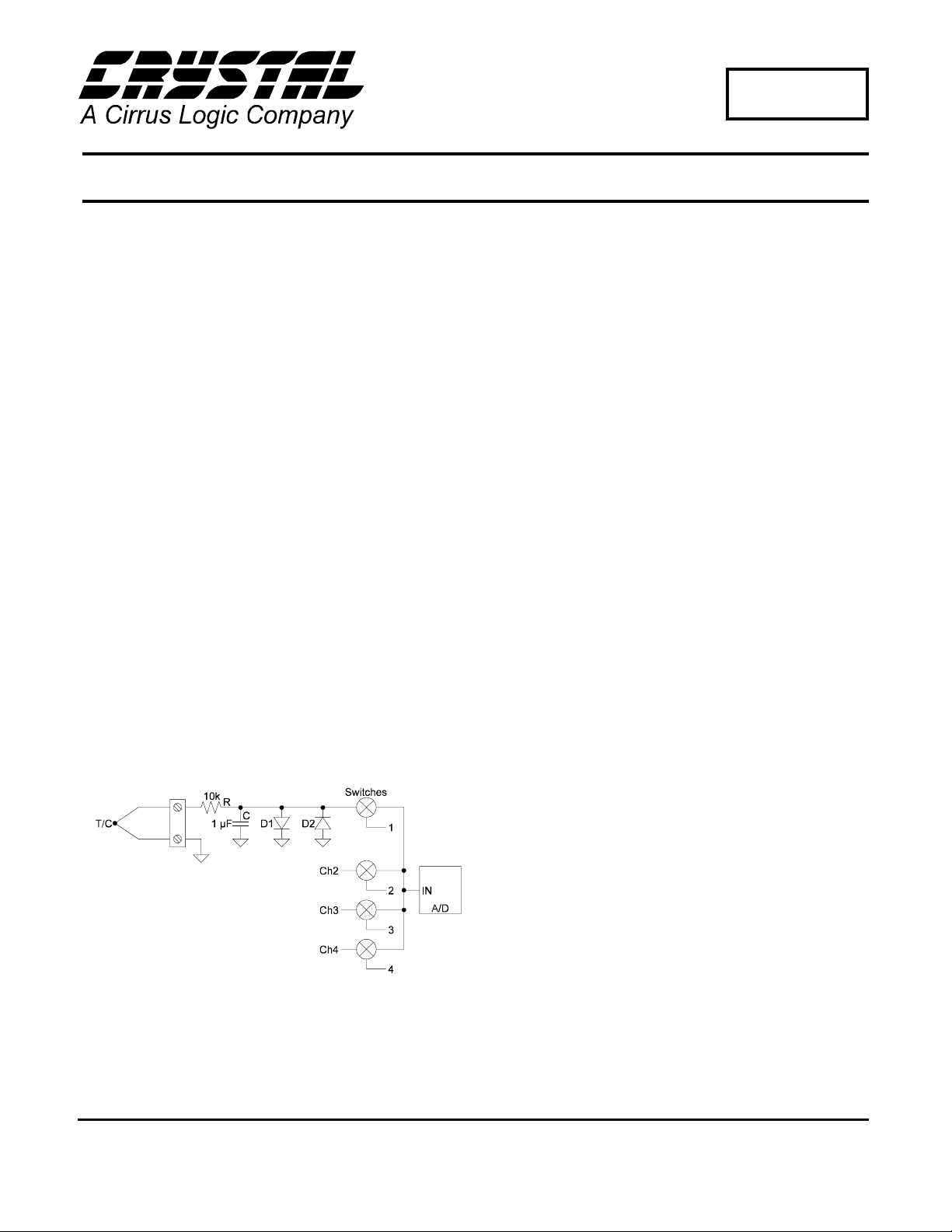
signal path. Figure 1 illustra tes a mult iplexed thermocouple circ uit which include s input protectio n.
Resistor R, capacitor C, and diodes D1 and D2 provide input protection for the analog switch and the
A/D converter. Input protection guards against
ESD (Electro-Static Discharge), high voltage
glitches wh ich can get couple d into long thermo couple leads in an industrial env ironment, an d incorrect conn ections which c an cause +24 vol ts to
become directly connected to the digitizer input
terminals.
To achie ve sufficien t protection , the input protection resistor is usually 10 KΩ or greater. This resistance can intro duc e m easure ment erro rs if l eaka ge
currents in the circuitry are large. Even small
changes in leakage currents can affect accuracy
since thermocouple output voltages change very
little for each degre e of tem perature c hange (ty pi-
cally betw een 6 µV/°C and 80 µV/°C). Th erefore,
leakage current from the analog switch or from the
input of the a mplifier us ed to ampl ify the th ermocouple sign al can introduce signi ficant errors if a
large protec tion resistor is used. A large value for
the protection resistor is desirable because the combination of R and C also act a s a low pass filte r to
help reject 50/60 Hz. A large resistor value helps to
achieve a low freque ncy cutoff for the filter while
using a small capacitor value (many applications
use surface mounted components in which the
availabi lity of su rface mount e d capa ci tors is li mit ed to low values ). The capacitor is usua lly a low
leakage device with a qu ality dielec tric to ach ieve
low dielectric absorp ti on.
Figure 1. Typical Thermocouple
Digitizer Input Circuitry
Crystal Semiconductor Corporation
P.O. Box 17847, Austin, Texas 78760
(512) 445 7222 FAX: (512) 445 7581
http://www.crystal.com
Figure 2 illu strates the C S5525/CS55 26 using the
p-channel J177 (or SST177 for surface mount)
JFET as an analog switch. The J177 has a maximum V
of 2.25 V, therefore a +5 V drive sig-
GS(off)
nal from one of the digital outputs from the
CS5525/CS5526 can turn it off (Driving the gate of
the JFET with only +3.0 volts will shut the J177 off
but it can exhibit more leakage current). When the
logic drive to the ga te of the JFET is 0 V, the FET
will be turned on. It can safely handle input signals
of ±250 mV without forward biasing the channel to
Copyright Crystal Semiconductor Corporation 1997
(All Rights Reserv ed)
MAY ‘97
AN75REV2
1
Page 2

Figure 2. CS5525/CS5526 Controls P-Channel
JFETs as analog switches.
gate junction. When ON, the J177 (SST177) exhibits a resistanc e of 300 ohms maximum. If u sed to
switch signals less than ±250 mV, the leaka ge cur rent (25 °C) will be sub-picoamps.
AN75
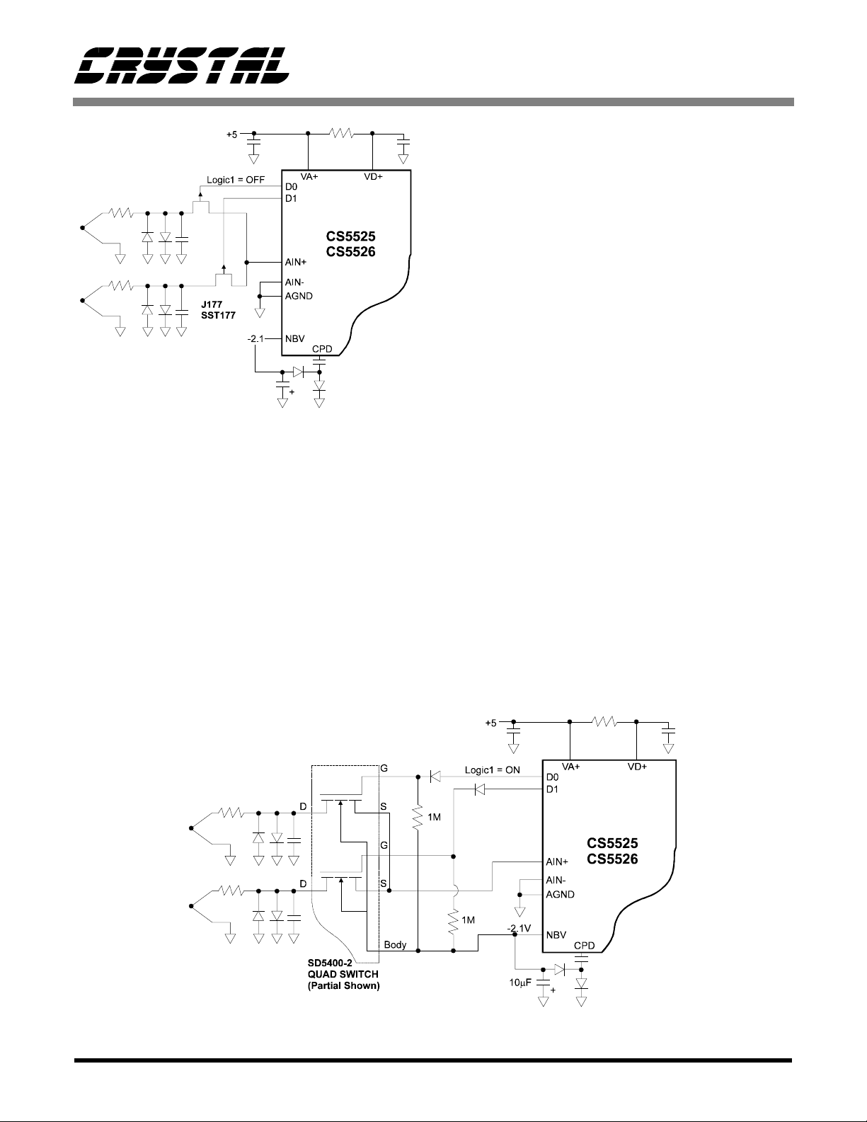
the CS5525/CS5 526 is low. The -0.6V gate drive
shuts off the tran sistor with adeq uate ga te drive to
ensure very high off resistance. When the D0-D3
output drive is high, the transistor is on with a resistance less tha n 100 Ω. Signals of ±1 V can readily
be passed by the switch.
Some analog switches are available which are designed to function with supply voltages of ±5 V or
less. The Advanced Linear Devices ALD4201 quad
switch is used in Figure 4 (1/2 of dev ice is shown)
for switching the rmocouple signa ls. The switch i s
operated from a +5 V supply and from the NBV
voltage (-2.1) used for the CS5525/CS5526. This is
acceptable as the supply current requirement of the
ALD4201 is only a microampere. Leakage currents
for the ALD4201 are stated to remain below 500
pA over the industrial temperature range. On resistance over the industrial t emperature range with a
total supply of +5V or more is less than 300 Ω.
Figure 3 illustrates an example of using an enhancement mode transistor switch as an analog
switch. The SD5400-2 quad DMOS switch is illustrated (the SD5000-2, SD5200-2, and SD5300-2
series are similar). The diode-resistor drive combination on the gate of the SD5400-2 allows the gate
to go to -0.6 V when the DO -D3 logic dr ive from
This application note illustrates the flexibility of
using the CS5525/CS5526 digital output pins to
control analog switches and multiplexers. While all
the circuits introduced have illustrated the CS5525/
CS5526 being used in thermoc ouple applica tions,
the device can be used for bridge transducers as
well.
Figure 3. CS5525/CS5526 Controls N-Channel DMOS transistors as analog switches.
2 AN75REV2
Page 3

Figure 4. CS5525/CS5526 Controls the low-voltage ALD4201 analog switch.
AN75
Figure 5 illustrates the CS5525/CS5526 configured
to interface to a bridge transducer. The bridge is excited with +5 V. The voltage reference for the A/D
is derived from th e +5 V which excite s the bridge
to set up a rati omet ric m easure men t confi gu ratio n.
A ALD4201 quad a nalog switch is used to select
between the differential bridge sign al and a thermistor tempera ture sensor which is be ing used to
measure the bridge temperature.
The CS5525/ CS5526 has four dig ital outputs th at
can be used to control as many as 16 analog switches with the use of either the 74HC137 or 74HC237
1-of-8 Decoder/ Multiplex ers. The ma in diffe rence
between the t wo chips is that the 74HC 137 has active low outputs; the 74HC237 has active high outputs. Figure 6 illu strates how t he CS5525 /CS5526
digital outp uts (D0-D3) can be used to d erive 16
separate control lines using a pair of 74HC237s.
Figure 5. CS5525/CS5526 Controls the low-volta ge ALD4201 analog s witch.
AN75REV2 3
Page 4

AN75
Figure 6. Use external logic to generate 16 separate analog switch control lines.
APPENDIX
J177/SST177 Suppliers
Calogic, Fremont, California
Siliconix, Santa Cla ra , Ca l ifo rni a
Interfet, Garland, Texas
Philips, Eind h ov en , Th e Ne th erlands
SD5000-2 Series Supplier
Calogic, Fremont, California
ALD4201 Supplier
Advanced Linear De vices, Sunnyvale, Ca lifornia
4 AN75REV2
 Loading...