

Page 1
Interfacing the CS5525/6/9 to the 80C51
INTRODUCTION
AN74
Application Note
By Keith Coffey
This applica tion note details the interfac e of Crys-
tal Semiconductor’s CS5525/6/9 Analog-to-Digital Conver ter (ADC ) to an 80C51 mi croc ontrol ler.
This note take s the reade r through a simple e xample describing how to communicate with the ADC.
All algorithms discussed are included in the Ap-
pendix at the end of this note.
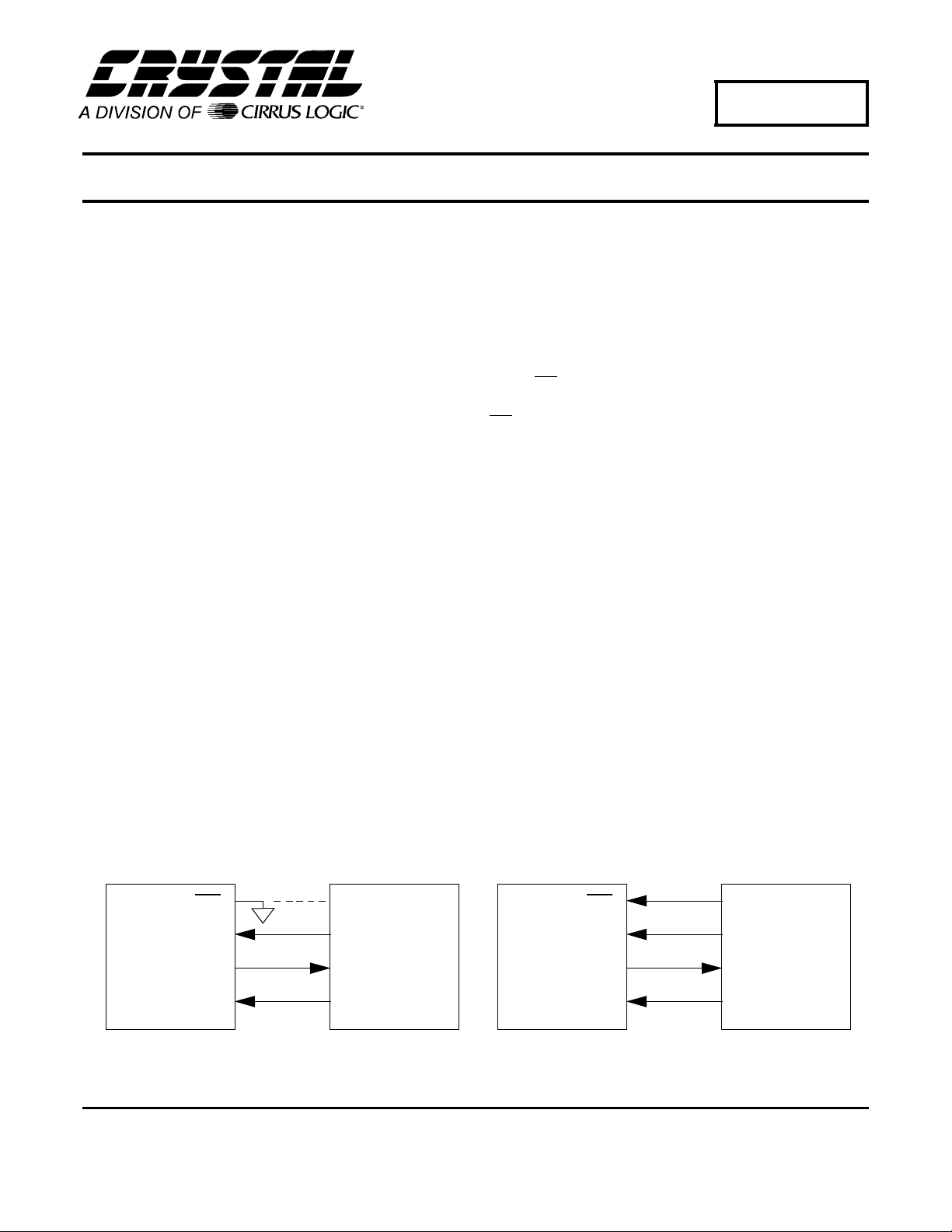
ADC DIGITAL INTERFACE
The CS5525/6/9 interfaces to the 80C51 through
either a thre e-wir e or a four-wir e inte rface. Figure
1 depicts the interface between the two devices.
Though this software was written to interface to
Port 1 (P1) on the 80C51 with a four-wire interface,
the algorithms can be easily modified to work with
the three-wire format.
The ADC’s serial port consists of four control
lines: CS
CS
, SCLK, SDI, and SDO.
, Chip S elect, is the contro l line w hich e nables
access to the serial port.
SCLK, Serial Clock, is the bit-clock which controls
the shifting of data to or from the ADC’s serial
port.
SDI, Serial Data In, is the data signal used to transfer data from the 80C51 to the ADC.
SDO, Serial Data Out, is the data signal used to
transfer outpu t da ta from the ADC to the 80C 51.
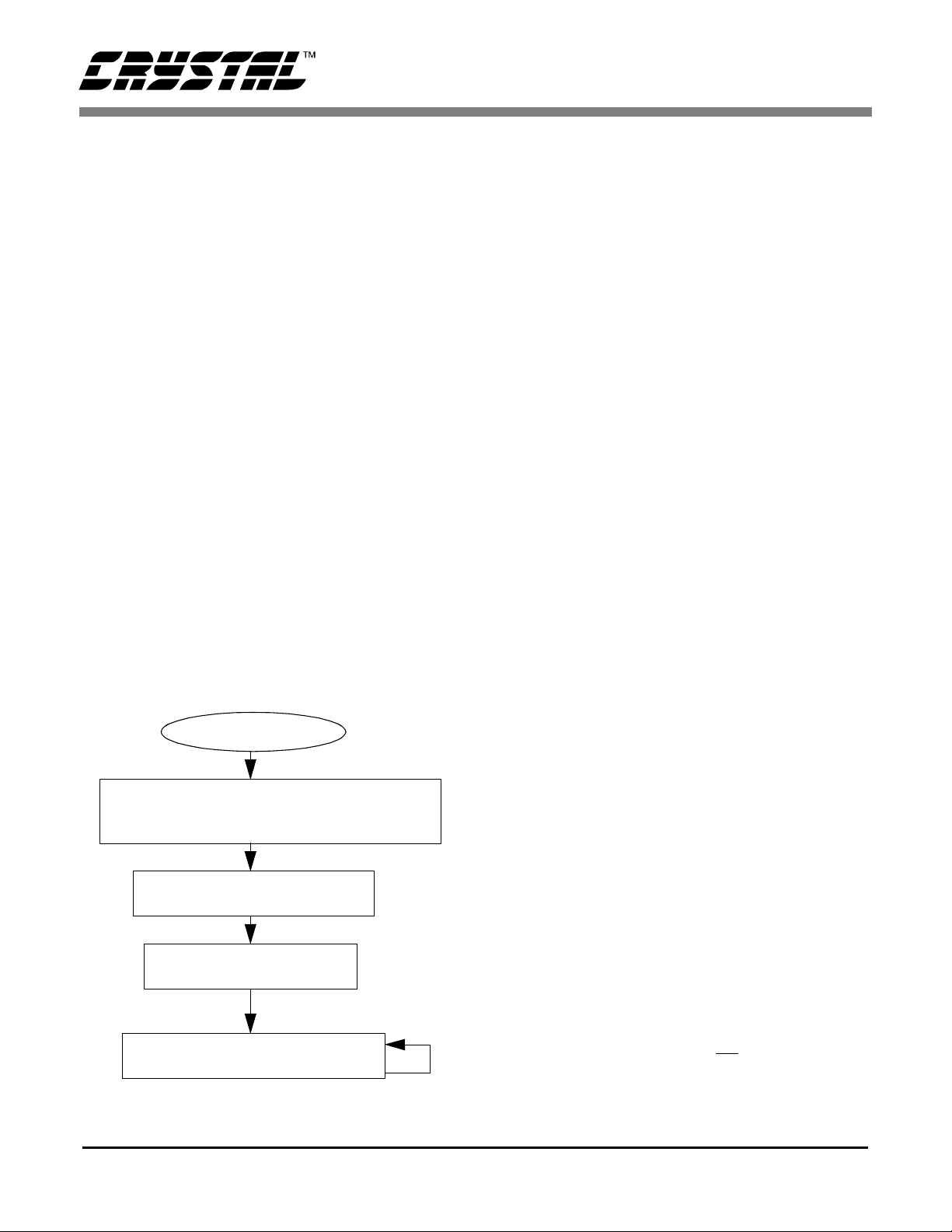
SOFTWARE DESCRIPTION
This note presents algorithms to initialize the
80C51 and the CS5525/6/9, perform self-offset calibration, modify the CS5525/6/9’s gain register,
and acquir e a c onversi on. Fi gure 2 depi cts a block
CS5525/6/9 80C51
CS
SDI
SDO
SCLK
Cirrus Logic, Inc.
Crystal Semiconductor Products Division
P.O. Box 17847, Austin, Texas 78760
(512) 445 7222 FAX: (512) 445 7581
http://www.crystal.com
P1.0 (logic 0)
P1.1
P1.2
P1.3
CS5525/6/9 80C51
CS
SDI
SDO
SCLK
Figure 1. 3-Wire and 4-Wire Interfaces
Copyright Cirrus Logic, I nc. 1997
(All Rights Reserv ed)
P1.0
P1.1
P1.2
P1.3
NOV ‘97
AN74Rev2
1
Page 2
AN74
diagram. While reading this application note,
please refer to the Appendix for the code listing.
Initialize
Initialize is a subroutine that configures P1 (Port 1)
on the 80C5 1 and places th e CS5525/6/9 into t he
command-state. First, P1’s data direction is configured as depicted in Figure 1 (for mo re infor ma tion
on configuring ports refer to 80C51 Data Sheet).
After configurin g the port, the controller enters a
delay state to allow time for the CS5525/6/9’s power-on-reset and oscillator to start-up (oscillator
start-up ti me i s typi ca lly 5 00ms). The last st ep is t o
reinitialize the serial port on the ADC (reinitializing the serial port is unnecessary here, the code was
added for demonstration purposes only). This is
implemented by sending the converter sixteen
bytes of logic 1’s fol lowed by on e fina l byte, with
its LSB at logic 0. On ce sent, th e sequenc e places
the serial port of the ADC into the com mand-state,
where it awaits a vali d command.
After retuning to main, the software demonstrates
how to calibra te the converter’s offset.
START
INITIALIZE
MICROCONTROLLER & CS5525/6/9
SELF-OFFSET CAL.
MODIFY GAIN
ACQUIRE CONVERSION
Figure 2. CS5525/6/9 Software Flowchart
Self-Offset Calib r ation
Calibrate is a subroutine that calibrates the converter’s offset. Calibrate first sends 0x000001
(Hex) to the conf iguration register. This i nstructs
the converter to perform a self-offset calibration.
Then the Done Flag (D F) bit in th e configuration
register i s polled until set. Onc e DF is set, it indicates that a valid calibration was performed. To
minimize digital noise (while performing a calibration or a c onver sion ), ma ny sy ste m d esigners may
find it advantageous to add a software delay equivalent to a conversion or calibration cycle before
polling the DF bit.
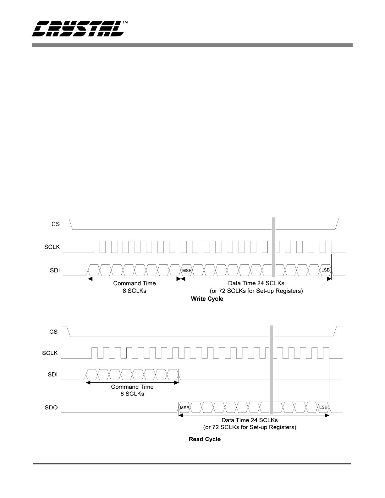
Read/Write Gain Register
To modify the gain register the command-byte and
data-byte variables are first initialized. Then the
subroutine write_to_register uses these variables to
set the cont ents of the gain register in the CS5525/
6/9 to 0x800000 (HEX). To do this,
write_to_register calls transfer_byte four times
(once for t he command byte an d three additional
times for the 24 bits of data). Transfer_byte is a
subroutine used to ‘bi t-bang’ a byte of inform ation
from the 80C51 to the CS5525/6/9. A byte is transferred one bit at a time, MSB (most significant bit)
first, by pl a ci ng a bit of i nformation on P1.1 (SDI)
and then pulsing P1.3 (SCLK). The byte is transferred by repeating this process eight times. Figure
3 depicts the ti min g diag ra m for t he wri te-c ycle in
the CS5525/ 6/9’s serial port. This al gorithm dem onstrates how to write to the g ain register. It does
not perform a gai n calibration. T o perform a gain
calibration, follow the procedures outlined in the
data sheet.
To verify that 0 x800000(HEX) wa s written to the
gain register, read_register is call ed. It dup licates
the read-cycle timing diagram depicted in Figure 4.
Read_register first asserts CS
. Then it calls
transfer_byte once to transfer the command-byte to
the CS552 5/6/9 . This pla ces th e conv erter in to the
2 AN74Rev2
Page 3
AN74
data-state where it wa its unt il data is rea d from its
serial port. Read_register then calls receive_byte
three times and transfers three bytes of information
from the CS5525/6/9 to the 80C51. Similar to
transfer_byte, receive_byte acq uires a byte one bit
at a time MSB first. When the transfer is complete,
the variables high_byte, mid_byte, and low_byte
contain the CS5525/6/9’s 24-bit ga in register.
Acquire Conversion
To acquire a conversion the subroutine
acquire_conversion is called. To prevent from corrupting the configuration register
acquire_conversion first instructs the 80C51 to
save the contents of configuration register. This information is stored in the variable high_byte,
mid_byte and low_byte. Th en, PF (Port Fl ag, the
fifth bit in t he config urati on regist er which is now
represented a s bit five in the variable low-byte) i s
masked to logic 1. When PF is set to logic 1, SDO’s
function is modified to fall to logic 0 signaling
when a conversion is complete and ready to acquire
(refer to Figure 5). After the PF is set,
acquire_conversion sends the command-byte
0xC0 to the converter instructing it to perform a
single conversion. From there, acquire_conv er sion
calls the subroutine toggle_ s do. Toggle_sdo is rou-
tine that polls P1.2 (SDO) until its logic level drops
to logic 0. After SDO falls, toggle_sdo pulses P1.3
(SCLK) eight times to clear the SDO signal flag.
After the SDO flag is cleared, the 80C51 reads the
conversion data word. Figu re 6 depicts ho w 16-bit
and 20-bit conv e rsion words are stored.
Figure 3. Write-Cycle Timing
Figure 4. Read-Cycle Timing
AN74Rev2 3
Page 4
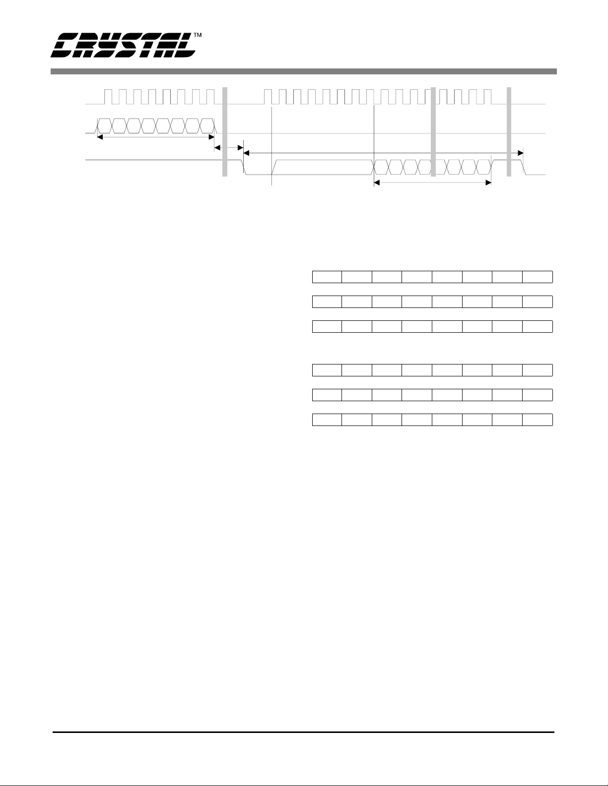
SCLK
SDI
*
t
ommand Time
C
8SCLKs
DO
S
td = XIN/OWR clo ck cycles for each conversion except the
*
first conversion which will take XIN/OWR + 7 clock cycles
d
Data SDO Continuous Conversion Read (PF bit = 1)
Figure 5. Conversion/Acquisition Cycle with PF Bit Asserted
SCLKs Clear SDO Flag
8
AN74
IN/OWR
X
Clock Cycles
SB
M
ata Time
D
24 SCLKs
SB
L
An alternative method can be used to acquire a conversion. By clearing the Port Flag bit, the serial
port’s function isn’t modified. Th e Done Flag bit
(bit three in the configuration register) can be
polled as it indicates when a conversion is compete
and ready to acquire. The conversion is acquired by
reading the conversion data register.
MAXIMUM SCLK RATE
A machine cycle in the 80C51 consists 12 oscillator
periods or 1µs if the microcontroller’s oscillator
frequency is 12 MHz. Since the CS5525/6/9’s maximum SCLK rate is 2MHz, additional no operation
(NOP) delays may be necessary to reduce the transfer rate if the microcontroller system requires higher rate oscillator s.
DEVELOPMENT TOOL DESCRIPTION
The code in the application note was developed using a software development package from Franklin
Software, Inc. The code consists of intermixed C
and assemb ler algor ithm s which a re sub sets of the
algorithms use d by the CDB5525/ 6/9, a customer
MSB High-Byte
D19 D18 D17 D16 D15 D14 D13 D12
Mid-Byte
D11 D10 D9 D8 D7 D6 D5 D4
Low-Byte
D3 D2 D1 D0 0 0 OD OF
A) 20-Bit Conversion Data Word
MSB High-Byte
D15 D14 D13 D12 D11 D10 D9 D8
Mid-Byte
D7 D6 D5 D4 D3 D2 D1 D0
Low-Byte
111100ODOF
B) 16-Bit Conversion Data Word
0- always zero, 1
- always one,
OD - Oscillation Detect, OF - Overflow
Figure 6. Bit Representation/Storage in PIC16F84
evaluation board from Crystal Semiconductor.
Moreover, Frankli n’s A51 Assembler, C51 Compiler, and L5 1 Linker de velopment so ftware were
used to generat e the run-t ime software for the mi crocontrol ler on the CDB5526.
4 AN74Rev2
Page 5

AN74
CONCLUSION
This applicat ion note prese nts an example of how
to interface the CS552 5/6/9 to the 80C51 . It is divided into tw o main sections: hardware and software. The hardware interface illustrates both a
three-wire and a four-wire interface. The three-
TM
wire is SPI
and MICROWIRE
The software, developed with development tools
from Franklin Software, Inc., illustrates how to
write to the ADC’s internal register, read from the
ADC’s internal registers, and acquire a conversion.
The software is modularized and illustrates the im-
TM
compatible.
portant subroutines, e.g. write_byte, read_byte, and
toggle_sdo, each of which were written in assem-
bly language. This allows both assembly and C
programmers access to these modules.
The softwa re described in the note is include d in
the Appendix a t t h e e nd of this document .
TM
SPI
MICROWIRE
is a trademark of Motorola.
TM
is a tradem ark of Nati onal Sem i-
conductor.
AN74Rev2 5
Page 6

APPENDIX
80C51 Microcode to Interface to the CS5525/6/9
/****************************************************************************
* File: 55268051.asm
* Date: November 1, 1996
* Programmer: Keith Coffey
* Revision: 0
* Processor: 80C51
* Program entry point at routine "main".
****************************************************************************
* This program is designed as an example of interfacing a 80C51 to a CS5525/6/9
* Analog-to-Digital Converter. The program interfaces via Port 1 which controls the
* serial communications, calibration, and conversion signals.
****************************************************************************/
/*** Function Prototypes ***/
void initialize(void);
void reset_converter(void);
void toggle_sdo(void);
char receive_byte(void);
void transfer_byte(char);
void write_to_register(char command,char low,char mid, char high);
void read_regi st er( char command);
void acquire_conve rsion(char command);
AN74
/*** Byte Memory Map Equates ***/
sfr P1 = 0x90; /*Port One*/
sfr ACC = 0xE0; /*Accumulator Register Equate*/
/*** Bit Memory Map Equates ***/
sbit CS
sbit SDI = 0x91; /* Serial Data In*/
sbit SDO = 0x92; /*Serial Data Out*/
sbit SCLK = 0x93; /*Serial Clock*/
/*** Global Variable ***/
char command, /*Memory Storage Variable for Command Byte */
= 0x90; /* Chip Select, only used in four-wire mode*/
high_byte, /*Memory Storage Variable for Most Significant Byte*/
mid_byte, /* Memory Storage Variable for Most Significant Byte*/
low_byte, /* Memory Storage Variable for Most Significant Byte*/
temp, /*General Purpose Temporary Variable*/
mode; /*Variable Stores Mode of Operation 0 = three wire, 1 = 4 wire*/
6 AN74Rev2
Page 7

/**************************************************************************************
* Program Code
**************************************************************************************
* Routine - Main
* Input - none
* Output - none
* This is the entry point to the progr am
**************************************************************************************/
main() {
mode = 1; /*Make Communication be Four-Wire Mode*/
initializ e() ; /*Call Routine to Init ialize 80C51 and CS5525/6/9*/
while(1){
command = 0x82; /*Prepare to Write to Gain Register*/
high_byte = 0x80; /*Make High_byte 80 (HEX)*/
mid_byte = 0x00; /*Make Mid_byte all Zero’s*/
low_byte = 0x00; /*Make low_byte all Zero’s*/
write_to_register(command,low_byte,mid_byte,high_byte);/*Write to gain Register*/
read_register(0x92); /*Read Contents of Gain Register*/
while(1){
acquire_conversion(0xC0); /*Acquire a Single Conversion*/
}/*End inner while loop*/
}/*End While Loop*/
}/*end main*/
AN74
/*****************************Subroutines**********************************************/
/*************************************************************************************
* Routine - initialize
* Input - none
* Output - none
* This subroutine initializes Port 1 for interfacing to the CS5525/6/9 ADC.
* It provides a time delay for oscillator start-up/wake-up period.
* A typical start-up time for a 32768 Hz crystal, due to high Q, is 500 ms.
* Also 1003 XIN clock cycles are allotted for the ADC's power on reset.
**************************************************************************************/
void initialize()
/*** Local Variables ***/
data int counter;
/*** Body of Subroutine ***/
/*** Initialize 80C51’s Port 1 ***/
P1 = 0xF4; /*SCLK - Output */
/*SDI - Output */
/*SDO - Input */
/*CS
/*Initialize CS5525/6/9*/
/*Delay 2048 SCLK Cycles, to allow time for Oscillator start-up and power on reset*/
for(counter=0;counter<2047;counter++){
SCLK = 0x01; /*Assert SCLK*/
SCLK = 0x00; /*Deassert*/
}
- Output */
AN74Rev2 7
Page 8

/*Reset Serial Port on CS5525/6/9*/
SDI = 0x01; /*Assert SDI*/
for(counter=0;counter<255;counter++) {
SCLK = 0x01; /*Assert SCLK*/
SCLK = 0x00; /*Deassert SCLK*/
}
SDI = 0x00; /*Deassert SDI PIN*/
SCLK = 0x01; /*Assert SCLK*/
SCLK = 0x00; /* Deassert SCLK*/
}
/**************************************************************************************
* Routine - calibrate
* Input - none
* Output - none
* This subroutine instructs the CS5525/6/9 to perform self-offset calibration.
**************************************************************************************/
void calibrate()
{ write_to_register(0x84,0x01,0x00,0x00); /*Assert RS bit*/
/*Read C onfigura tion Regi ster Until DF Bit is Asserted*/
do {
read_register(0x94); /*Read Configuration Register*/
temp = low_byte&0x08; /*Mask DF bit to 1*/
} while (temp != 0x08);
read_register(0 x92); /*Deasserts DF Bit*/
}/*End calibrate */
AN74
/**************************************************************************************
* Routine - write_to _registe r
* Input - command, lowbyte, midbyte, highbyte
* Output - none
* This subroutine instructs the CS5525/6/9 to write to an internal register.
**************************************************************************************/
void write_to_register(char command,char low,char mid,char high){
if(mode == 1) P1 = 0xF4; /*Assert CS
transfer_byte(command); /*Transfer Command Byte to CS5525/6/9*/
transfer_byte(high); /*Transfer High Byte to CS5525/6/9*/
transfer_byte(mid); /*Transfer Middle Byte to CS5525/6/9*/
transfer_byte(low); /*Transfer Low Byte to CS5525/6/9*/
if(mode == 1) P1 = 0xF5; /*Deassert CS
}
if necessary*/
if necessary*/
8 AN74Rev2
Page 9

/**************************************************************************************
* Routine - read_register
* Input - command
* Output - low_byte, mid_byte, high_byte
*
* This subroutine reads an internal register of the ADC
/**************************************************************************************/
void read_regi st er( char command){
if(mode == 1) P1 = 0xF4; /*Assert CS
transfer_byte(command); /*Transfer Command Byte to CS5525/6/9*/
high_byte = receive_byte(); /*Receive Command Byte from CS5525/6/9*/
mid_byte = receive_byte(); /*Receive Command Byte from CS5525/6/9*/
low_byte = receive_byte(); /*Receive Command Byte from CS5525/6/9*/
if(mode == 1)P1 = 0xF5; /*Deassert CS
}
/**************************************************************************************/
* Routine - acquire_conversion
* Input - command
* Output - Conversion results in memory locations HIGHBYTE, MIDBYTE and
* LOWBYTE. This algorithm performs only single conversions. If
* continuous conversions are needed the routine needs to be
* modified. Port flag is zero.
*
* HIGHBYTE MIDBYTE LOWBYTE
* 7 6 5 4 3 2 1 0 7 6 5 4 3 2 1 0 7 6 5 4 3 2 1 0
* 16-bit results MSB LSB 1 1 1 1 0 0 OD OF
* 20-bit results MSB LSB 0 0 OD OF
* This subroutine initiates a single conversion.
/**************************************************************************************/
void acquire_conve rsion(char command){
/*** Read Configuration Register to Prevent Previously Set Bits from being Altered ***/
read_register(0x94); /*Read Configuration Register*/
low_byte = low_byte|0x20; /*Assert Port Flag Bit*/
write_to_register(0x84,low_byte, mid_byte, high_byte);/*Actually Send Commands*/
if necessary */
if necessary */
AN74
/*Acquire a Conversion*/
if(mode == 1)P1 = 0xF4; /*Assert CS
transfer_byte(0xC0); /*Transfer Command to CS5525/6/9*/
toggle_sdo(); /*Clear SDO*/
high_byte = receive_byte(); /*Receive Command Byte from CS5525/6/9*/
mid_byte = receive_byte(); /*Receive Command Byte from CS5525/6/9*/
low_byte = receive_byte(); /*Receive Command Byte from CS5525/6/9*/
if(mode == 1) P1 = 0xF5; /*Deassert CS
}
AN74Rev2 9
if necessary*/
if necessary*/
Page 10

;****************************************************************
;* Routine - RECEIVE_BYTE
;* Input - none
;* Outpu t - Byte receiv ed is place d in R7
;* Description - This routine moves 1 byte from the CS5525/6/9 to the 80C51.
; It transfers the byte by acquiring the logic level on PORT1 BIT 2
; It then pulses SCLK high and then back low again
; to advance the A/D’s serial output shift register to the next bit.
; It does this eight times to acquire one complete byte.
; This function’s prototype in C is: char receive_byte(void);
;Note: This routine can be used three time consecutively to transfer all 24 bits
; from the internal registers of the CS5525/6/9.
;****************************************************************
$DEBUG
USING 0 ; Use register bank 0
TCOD SEGMENT CODE ; Define ROUT as a segment of code
PUBLIC RECEIVE_BYTE ; Make subroutine global
RSEG TCOD ; Make code relocatable
RECEIVE_BYTE:
MOV R1,#08 ; Set count to 8 to receive byte
AN74
LOOP: ; Receive the byte
MOV C,P1.2 ; Move bit to carry
RLC A ; Rotate A in preparation for next bit
SETB P1.3 ; Set SCLK
CLR P1.3 ; Clear SCLK
DJNZ R1,LOOP ; Decrement byte, repeat loop if not zero
MOV R7,A ; Byte to be return is placed in R7
RET ; Exit subroutine
END
10 AN74Rev2
Page 11

;****************************************************************
;* Routine - TRANSFER_BYTE
;* Input - byte to be transferred
;* Output - None
;* Description - This subroutine transfers 1 byte to the CS5525/6/9
; It transfers the byte by first placing a bit in PORT1 BIT 1.
; It then pulses the SCLK to advance the A/D’s serial
; output shift reg ister to th e next bit.
; It does this eight times to transmit one complete byte.
; The function prototype is: void TRANSFER_BYTE(char);
;Note: This routine can be used three time consecutively to transfer all 24 bits
; from the 80C51 to the internal registers of the CS5525/6/9.
;****************************************************************
$DEBUG
USING 0 ; Use register bank 0
TCOD SEGMENT CODE ; Make TCOD a segment of code
TDAT SEGMENT DATA ; Make TDAT a segment of data
PUBLIC TRANSFER_BYTE ; Make subroutine global
PUBLIC ?TRANSFER_BYTE?BYTE ; Make subroutine global
RSEG TDAT ; Make code relocatable
?TRANSFER_BYTE?BYTE:
VAR: DS 1 ; Define a storage location
RSEG TCOD ; Make code relocatable
TRANSFER_BYTE:
MOV A,VAR ; Move byte to be transmitted to ACC
MOV R1,#08 ; Set count to 8 to transmit byte
CLR P1.3 ; Clear SCLK
AN74
loop: ; Send Byte
RLC A ; Rotate Accumulator, send MSB 1st
MOV P1.1,C ; Transmit MSB first through C bit
SETB P1.3 ; Set SCLK
CLR P1.3 ; Clear SCLK
DJNZ R1,loop ; Decrement byte, repeat loop if not zero
CLR P1.1 ; Reset SDI to zero when not transmitting
RET ; Exit subroutine
END
AN74Rev2 11
Page 12

;****************************************************************
;* Routine - TOGGLE_SDO
;* Input - none
;* Output - none
;* Description - This routine reset the DRDY pin by toggling
;* SCLK 8 times after SDO falls.
; This routine polls SDO, waits for it to be asserted, then clears SDO
; for next conversion by pulsing SCLK eight times after SDO falls
; This functions prototype in C is: void toggle_sdo(void);
;****************************************************************
$DEBUG
USING 0 ; Use register bank 0
TCOD SEGMENT CODE ; Define Rout as a segment of code
PUBLIC TOGGLE_SDO ; Make subroutine public
RSEG TCOD ; Make code relocatable
TOGGLE_SDO:
MOV R1,#08 ; Setup counter
CLR P1.1 ; Clear SDI
JB P1.2,$ ; Poll SDO
loop:
SETB P1.3 ; Set SCLK
CLR P1.3 ; Clear SCLK
DJNZ R1,loop ; Decrement byte, repeat loop if not zero
RET ; Exit Subroutine
END
AN74
12 AN74Rev2
Page 13

• Notes •
Page 14

 Loading...