

Page 1

Application Note
USING THE CDBCAPTURE SYSTEM
WITH EMBEDDED A/D CONVERTERS
by
John Lis
AN44
INTRODUCTION
The CDBCAPTURE system can be used to
collect data from embedded Analog to Digital
Converters (ADCs). Thus system performance of
the analog front end can be measured, analyzed
and quantified. By analyzing the measured
performance, noise sources can be identified,
isolated, and corrective actions taken. Here
CDBCAPTURE is used as an engineering tool,
reducing development time during system test
and integration. Another application could be
using CDBCAPTURE in production for testing
finished products and verifying system
performance.
CDBCAPTURE
The CAPTURE interface board is a development
tool that interfaces a Crystal Semiconductor
ADC to a PC compatible computer. Digital data
from the ADC is collected in a high speed
digital FIFO, then transmitted to the PC over a
serial COM port. Evaluation software is included
to analyze the data and demonstrate the ADC’s
performance. The entire system consists of a
CAPTURE interface board, serial cable, RS232
cable, and software.
The software included with the CDBCAPTURE
system quantifies static and dynamic
performance of ADC systems. Static testing
includes Histogramming and calculation of the
mean, standard deviation and variance. Dynamic
testing includes Fast Fourier Transforms and
analysis of the power spectrum. Here Signal to
Noise Ratio (SNR), Signal to Noise plus
Distortion (SINAD), Signal to Distortion Ratio
(SDR), and Signal to Peak Noise (SPN) figures
are calculated. Time domain plots are available
to visualize signals in the time domain and
confirm operation.
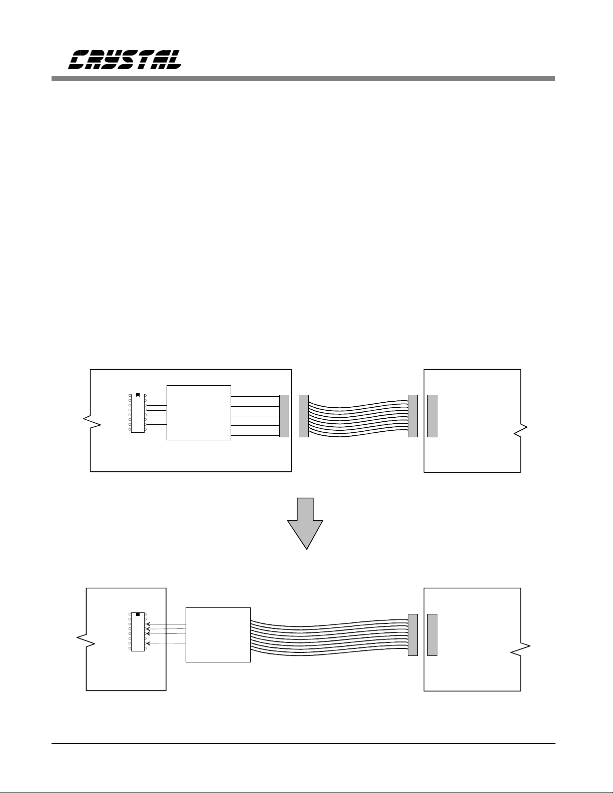
CDBCAPTURE WITH EMBEDDED ADCs
The CDBCAPTURE circuit board is designed to
directly interface with most Crystal
Semiconductor ADC evaluation boards. This
permits a quick and ea sy method to quantify and
verify the ADC’s performance. However, it is
often desirable to measure the ADC’s
performance in the actual system or to measure
the overall system performance. To collect data
from an embedded ADC, a special serial cable
needs to be designed. This cable incorporates the
digital interface circuitry which exists on the
evaluation board. This cable is connected to the
appropriate signals on the ADC.
To collect data from an embedded ADC, the
digital inte rface circuit ry on the e valuation boa rd
needs to be incorporated on a modified serial
Crystal Semiconductor Corporation
P.O. Box 17847, Austin, TX 78760
(512) 445-7222 FAX 445-7581
http://www.crysta l.com
Copyright Crystal Semiconductor Corporation 1996
(All Rights Reserved)
FEB ’95
AN44REV2
1
Page 2
Using The CDBCapture System with Embedded A/D Converters
cable. Figure 1 is a block diagram illustrating
the process. On the top of Figure 1, the
evaluation board CDBXXXX contains digital
interface circuitry which translates signals from
the ADC to three standard serial signals named
FRAME, SCLK and SDATA. The timing and
format of these signals vary from device ty pe to
device type .
In an embedded ADC application, the digital
interface circuit, between the ADC and the
CDBCPATURE circuit card, should be
implemented on a small card attached to the
serial cable as shown at the bottom of Figure 1.
The appropriate digital input signals need to be
identified. A method to connect to these signals
from the embedded system to the cable is then
CDBXXXX EVALUATION BOARD CDBCAPTURE
5 V
A
D
C
INTERFACE
CIRCUIT
GND
FRAME
SCLK
SDATA
implemented. The connection scheme varies for
each application and is easy to implement.
The schematic for the digital interface circuitry
is provided with th e evaluation board data sheet.
Locate the serial interface connector containing
the signals: +5 V, GND, FRAME, SCLK, and
SDATA on the schematic. Working from this
connector, back to the ADC, identify the
circuitry required to create the serial signals.
This circuitry is implemented on a separate
circuit board, attached to a 10 conductor ribbon
cable with an IDC socket for its CDBCAPTURE
interface. The ADC interface can be any
connector scheme that is easy to implement.
Possible alternatives include stake headers, test
clips, circular connectors, or "D" style
connectors.
SERIAL RIBBON
CABLE
EMBEDDED ADC CDBCAPTURE
A
D
C
2 AN44REV2
INTERFACE
CIRCUIT
Figure 1. CDBCAPTURE INTERFACE
MODIFIED
SERIAL RIBBON
CABLE
Page 3
Using The CDBCapture System with Embedded A/D Converters
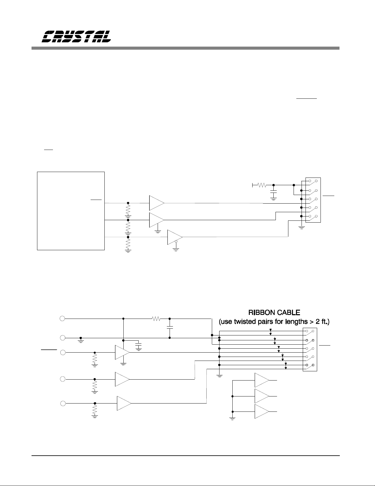
CS5508 EXAMPLE
The following example uses a CS5508 to
illustrate the process of designing a modified
serial cabl e. By examining the schematic for the
CDB5508 evaluation board, the digital interface
circuitry is identified. The schematic for the
CDB5508 evalu ation board is pro vided in Figure
1 of the CDB5505/6/7/8 data sheet. The digital
interface portion is shown in Figure 2 below.
Resistors R23, R24 and R25 are not required if
the
CS is always active. Also, U3B is always
U1
CS5505
CS5506
CS5507
OR
CS5508
DRDY
SDATA
SCLK
16
15
14
R23
100k
R24
100k
R25
100k
U2E
U2F
1211
1514
8
5
U3B
active when using the CAPTURE board, thus it
can be changed to a general purpose buffer such
as U2.
Figure 3 shows the schematic for the modified
cable derived fro m Figure 2. The
DRDY, SCLK
and SDATA signals are buffered to create the
serial cable signals for the CAPTURE board.
Five volt power is obtained from the embedded
system and filtered by R1 and C1 before it is
provided to the CAPTURE board. C2 is a
bypass capacito r for U1.
R22
+5
6
4
10
+
C16
10 uF
+5
+5
DRDY
SCLK
SDATA
+5 V
GND
DRDY
SCLK
SDATA
Figure 2. CDB5508 Evaluation Board Schematic for the Digital Interface
R1
+
HC4050
R2
100k
R3
100k
R4
100k
10
C2
0.1 uF
1
23
U1A
8
45
U1B
7
6
U1C
C1
10 uF
9
11
14
U1D
U1E
U1F
10
12
15
Figure 3. Modified Serial Cable Implementation of the Digital Interface
+5
+5
DRDY
SCLK
SDATA
AN44REV2 3
Page 4

Using The CDBCapture System with Embedded A/D Converters
Figure 4 shows how the hardware can be
implemented. The digital interface circuitry is
built upon a small circuit board. A ribbon cable
with a 10 circuit IDC socket is used for the
CDBCAPTURE interfac e. Separate ground wires
should be used for each signal return, and
twisted pa ir ribbon cable u sed fo r lengths greater
than two feet. The embedded interface uses
color coded test clips. The test clips provide a
means of interfacing an ADC without any
special connectors designed in the system.
However this method requires a little more setup
time, since the appropriate signals need to be
located on th e circui t board.
CS5102A EXAMPLE
The CS5102A is used in the second example of
an embedded application. The methodology for
the cable design is the same as that in the first
example usin g the CS5508. The digital interface
circuitry is obt ained from the CDB51 01A/5102A
evaluation board data sheet. This information is
contained in the evaluation board’s data sheet
U1
CS5101A
or
CS5102A
SDATA
SCLK SCLK
SSH/SDL
TRK1
TRK2
SDATA
SCLK
Figure 4. Construction of the Modified Serial Cable
+5V
JP4
1
3
5
HDR8D
+
C47
10 uF
+5V
2
4
6
BOTH
CH2
CH1
SDATA
SSH/SDL
TRK1
TRK2
.1 uFC48
15
14
1
2
6
U12
OE1
OE2
A0
A2
A5
74HC365
Y2
Y0
Y5
7
3
13
SSH/SDL
+5V
TRK2
TRK1
R3
10
TP00
R16
10k
8
JP5
HDR10D
9
U2
10
+5V
+5V
+5V
SLATCH
SCLK
SDATA
U3
10
S
11
CLK
12
D
13
R
74HC74
9
Q
8
4
5
U2
6
Figure 5. CDB5102A Evaluation Board Schematic for the Digital Interface
4 AN44REV2
Page 5

Using The CDBCapture System with Embedded A/D Converters
Figures 4, 5 and 6. The digital inte rface circuitry
for the CS5102A is s how in Figure 5.
Figure 6 is the way the digital circuitry is
implemented on the modified serial cable.
Figure 7 is the hardware implementation of the
modified serial cable shown in Figure 6. In this
P1
+5V
GND
TRK1
TRK2
SSH/SDL
SCLK
SDATA
JP1
R1
10k
BOTH
CH1
CH2
+5V
10
9
13
12
74HC74
10
11
12
13
U2-C
U2-B
S
D
R
+
U3B
8
11
C1
0.1 µF
Q
C2
+
0.1 µF
9
8
74HC00
1
U2A
2
example, the embedded system is designed with
a test connector. The modified serial cable is
built with a conne ctor which mates to t he syst em
test connector. The test connector provides a
convenient and reliable means of interfacing the
ADC.
R3
C3
10
4
3
U2B
5
+
10 µF
6
+5V
U3A
4
3
2
1
5
S
Q
D
6
R
P2
+5V
+5V
SLATCH
SCLK
SDATA
Figure 6. Modified Serial Cable Implementation of the Digital Interface
Figure 7. Construction of the Modified Serial Cable
AN44REV2 5
Page 6

Using The CDBCapture System with Embedded A/D Converters
Testing An Embedded ADC
System performance can be measured by
interfacing the embedded ADC. The previous
sections described the hardware modification
required to interface a Crystal Semiconductor
ADC with the CAPTURE board. Figures 8, 9,
and 10 are the results of using the histogram tes t
on a CS5101A in an embedded system.
Figure 8 is a histogram of a CS5101A ope rating
in the bipolar mode with the analog input pin
grounded right at the package. Data book
performance is expected, if proper design
practices have been used in developing the
circuit an d layout. In Figure 8, t he mean is -0.69
counts, which is well within the typical
specification o f two counts for the bipolar offset.
The standard deviation is 0.49 counts. This
translat es to 67 uV
( 0.49 x 9 volts ⁄
RMS
CS5101A data s heet specifie s 70 uV
16
). The
2
RMS typical.
Figure 8. Histogram of a CS5101A with the Input
Grounded
A buffer op-amp is integrated in the system and
a data set is collected and displ ayed in Figure 9.
Both the mean and standard deviation numbers
changed with the addition of the op-amp. The
op-amp added 0.66 counts to the offset or
91 uV. The RMS noise increased to 0.63 counts
or 87 uV.
Figure 10 shows the histogram for the ADC,
buffer op-amp, and signal source. The signal
source outpu t is set at zero volts. The histogram
statistics indicate an o ffset of 1.59 count s or 218
uV and the RMS noise is at 218 uV. Note, that
as more components are added to the system, the
offset changes and the noise increases. These
changes can be used to isolate and identify
problems.
Figure 9. Hist ogram of a CS51 01A with a Buff er Op-Amp
Figure 10. Histogram of a CS5101A with a Signal Source
6 AN44REV2
Page 7

Using The CDBCapture System with Embedded A/D Converters
CONCLUSION
The CDBCAPTURE system is designed to
easily connect to most Crystal Semiconductor
ADC evaluation boards. Digital circuitry is
included on the evaluation boards to implement
a standard serial data bus. The CAPTURE board
is software reconfigurable to adjust for different
ADCs and fu ture products. Th e CDBCAPTURE
system permits easy transfer of digital data to a
PC for analysis.
Many times it is desirable to collect data from
the ADC while it is operating inside a complete
acquisition system. In this case, the digital
interface circuitry for the CAPTURE board is
implemented outside the system on a modified
cable. The electrical system has to provide the
appropriate interconnect scheme, using either
connectors or test poin ts to clip o nto.
The modified serial cable allows the user to
measure performance of the ADC while it is
embedded in an electrical system. The ADC as
well as the system performance can be measured
and quantified. This information is used to
isolate problems and investigate how certain
subsystems interact with each other.
AN44REV2 7
Page 8

Using The CDBCapture System with Embedded A/D Converters
• Notes •
8 AN44REV2
 Loading...