

Page 1

AN374
Application Note
Considerations for Light Engine Selection
for a CS1630/31 2-Channel TRIAC Dimmable Circuit
1 Overview of the CS1630
The CS1630/31 is a high-performance offline AC to DC LED controller for dimmable and high color rendering index
(CRI) LED replacement lamps and luminaires. It features Cirrus Logic's proprietary digital dimmer compatibility control technology and digital correlated color temperature (CCT) control system that enables two-channel LED color
mixing.
The CS1630/31 offers tremendous flexibility to achieve constant CCT control to match an incandescent dimming
profile. The digital CCT control system provides the ability to program dimming profiles, such as constant CCT dimming and black body line dimming. The CS1630/ 31 optimizes LED color mixing by temperature compensating the
LED current with an external negative temperature coefficient (NTC) thermistor. The IC controller is equipped with
power line calibration for remote system calibration and end-of-line programming. The CS1630 provides a register
lockout feature for security against potential access to proprietary registers.
During the course of two-channel design, several design tradeoffs are made based on cost, size, and performance.
This document considers the requirements when designing a system around the CS1630/31. This document helps
answer the following system questions:
• How can the light engine be designed or modified to maximize the benefits of the CS1630/31?
• How can clear specifications be derived for the system and the LED driver that can reduce the light bulb
development time with the CS1630/31?
Further Reading
• See data sheet DS954 2-Channel TRIAC Dimmable LED Driver IC to review the features and
specifications of the CS1630/31
• See application note AN368 Design Guide for a CS1630/31 2-Channel TRIAC Dimmable SSL Circuit for
questions on how to design the LED driver using the CS1630/31
• See application note AN369 Device Programmer User Guide to review the CS1630/31 application software
and graphical user interface (GUI)
Cirrus Logic, Inc.
http://www.cirrus.com
Copyright Cirrus Logic, Inc. 2013
(All Rights Reserved)
FEB’13
AN374REV2
Page 2

AN374
Contacting Cirrus Logic Support
For all product questions and inquiries contact a Cirrus Logic Sales Representative. To find the one nearest to you
go to www.cirrus.com
IMPORTANT NOTICE
Cirrus Logic, Inc. and its subsidiaries ("Cirrus") believe that the information contained in this document is accurate and reliable. However, the information is subject
to change without notice and is provided "AS IS" without warranty of any kind (express or implied). Customers are advised to obtain the latest version of relevant
information to verify, before placing orders, that information being relied on is current and complete. All products are sold subject to the terms and conditions of sale
supplied at the time of order acknowledgment, including those pertaining to warranty, indemnification, and limitation of liability. No responsibility is assumed by Cirrus
for the use of this information, including use of this information as the basis for manufacture or sale of any items, or for infringement of patents or other rights of third
parties. This document is the property of Cirrus and by furnishing this information, Cirrus grants no license, express or implied under any patents, mask work rights,
copyrights, trademarks, trade secrets or other intellectual property rights. Cirrus owns the copyrights associated with the information contained herein and gives
consent for copies to be made of the information only for use within your organization with respect to Cirrus integrated circuits or other products of Cirrus. This consent does not extend to other copying such as copying for general distribution, advertising or promotional purposes, or for creating any work for resale.
CERTAIN APPLICATIONS USING SEMICONDUCTOR PRODUCTS MAY INVOLVE POTENTIAL RISKS OF DEATH, PERSONAL INJURY, OR SEVERE PROPERTY OR ENVIRONMENTAL DAMAGE ("CRITICAL APPLICATIONS"). CIRRUS PRODUCTS ARE NOT DESIGNED, AUTHORIZED OR WARRANTED FOR
USE IN PRODUCTS SURGICALLY IMPLANTED INTO THE BODY, AUTOMOTIVE SAFETY OR SECURITY DEVICES, LIFE SUPPORT PRODUCTS OR OTHER
CRITICAL APPLICATIONS. INCLUSION OF CIRRUS PRODUCTS IN SUCH APPLICATIONS IS UNDERSTOOD TO BE FULLY AT THE CUSTOMER'S RISK
AND CIRRUS DISCLAIMS AND MAKES NO WARRANTY, EXPRESS, STATUTORY OR IMPLIED, INCLUDING THE IMPLIED WARRANTIES OF MERCHANTABILITY AND FITNESS FOR PARTICULAR PURPOSE, WITH REGARD TO ANY CIRRUS PRODUCT THAT IS USED IN SUCH A MANNER. IF THE CUSTOMER
OR CUSTOMER'S CUSTOMER USES OR PERMITS THE USE OF CIRRUS PRODUCTS IN CRITICAL APPLICATIONS, CUSTOMER AGREES, BY SUCH USE,
TO FULLY INDEMNIFY CIRRUS, ITS OFFICERS, DIRECTORS, EMPLOYEES, DISTRIBUTORS AND OTHER AGENTS FROM ANY AND ALL LIABILITY, INCLUDING ATTORNEYS' FEES AND COSTS, THAT MAY RESULT FROM OR ARISE IN CONNECTION WITH THESE USES.
Use of the formulas, equations, calculations, graphs, and/or other design guide information is at your sole discretion and does not guarantee any specific results or
performance. The formulas, equations, graphs, and/or other design guide information are provided as a reference guide only and are intended to assist but not to
be solely relied upon for design work, design calculations, or other purposes. Cirrus Logic makes no representations or warranties concerning the formulas, equations, graphs, and/or other design guide information
Cirrus Logic, Cirrus, the Cirrus Logic logo designs, EXL Core, the EXL Core logo design, TruDim, and the TruDim logo design are trademarks of Cirrus Logic, Inc.
All other brand and product names in this document may be trademarks or service marks of their respective owners.
IMPORTANT SAFETY INSTRUCTIONS
Read and follow all safety instructions prior to using this demonstration board.
This Engineering Evaluation Unit or Demonstration Board must only be used for assessing IC performance in a
laboratory setting. This product is not intended for any other use or incorporation into products for sale.
This product must only be used by qualified technicians or professionals who are trained in the safety procedures
associated with the use of demonstration boards.
Risk of Electric Shock
• The direct connection to the AC power line and the open and unprotected boards present a serious risk of electric
shock and can cause serious injury or death. Extreme caution needs to be exercised while handling this board.
• Avoid contact with the exposed conductor or terminals of components on the board. High voltage is present on
exposed conductor and it may be present on terminals of any components directly or indirectly connected to the AC
line.
• Dangerous voltages and/or currents may be internally generated and accessible at various points across the board.
• Charged capacitors store high voltage, even after the circuit has been disconnected from the AC line.
• Make sure that the power source is off before wiring any connection. Make sure that all connectors are wel
connected before the power source is on.
• Follow all laboratory safety procedures established by your employer and relevant safety regulations and guidelines
such as the ones listed under, OSHA General Industry Regulations - Subpart S and NFPA 70E.
Suitable eye protection must be worn when working with or around demonstration boards. Always
comply with your employer’s policies regarding the use of personal protective equipment.
All components and metallic parts may be extremely hot to touch when electrically active.
2 AN374REV2
Page 3

AN374
TABLE OF CONTENTS
1 OVERVIEW OF THE CS1630 . . . . . . . . . . . . . . . . . . . . . . . . . . . . . . . . . . . . . . . . . . . . . . . . . . . . . . . . . . . . . . 1
2 INTRODUCTION . . . . . . . . . . . . . . . . . . . . . . . . . . . . . . . . . . . . . . . . . . . . . . . . . . . . . . . . . . . . . . . . . . . . . . . . 4
2.1 Definition of Acronyms . . . . . . . . . . . . . . . . . . . . . . . . . . . . . . . . . . . . . . . . . . . . . . . . . . . . . . . . . . . . . . . . 4
2.2 Definition of Symbols . . . . . . . . . . . . . . . . . . . . . . . . . . . . . . . . . . . . . . . . . . . . . . . . . . . . . . . . . . . . . . . . . 5
3 INTRODUCTION TO THE COLOR SYSTEM . . . . . . . . . . . . . . . . . . . . . . . . . . . . . . . . . . . . . . . . . . . . . . . . . . 6
4 LIGHT ENGINE CHOICES . . . . . . . . . . . . . . . . . . . . . . . . . . . . . . . . . . . . . . . . . . . . . . . . . . . . . . . . . . . . . . . . . 7
4.1 Considerations for the Color System . . . . . . . . . . . . . . . . . . . . . . . . . . . . . . . . . . . . . . . . . . . . . . . . . . . . . 7
Constraint 1: Translating current versus dim requirements into a fourth-order or lower polynomial. . . . . . 7
Constraint 2: The current versus dim plot should have intercept at origin . . . . . . . . . . . . . . . . . . . . . . . . . .7
Constraint 3: Placement of NTC with respect to light engine . . . . . . . . . . . . . . . . . . . . . . . . . . . . . . . . . . . .7
Constraint 4: Red currents increase with an increase in ambient temperature . . . . . . . . . . . . . . . . . . . . . .8
Constraint 5: Maximum allowable color gain is 4.0 . . . . . . . . . . . . . . . . . . . . . . . . . . . . . . . . . . . . . . . . . . .8
4.2 Constraints Imposed by Second Stage . . . . . . . . . . . . . . . . . . . . . . . . . . . . . . . . . . . . . . . . . . . . . . . . . . . 8
Constraint 1: Currents in either channel should not be zero at non-zero dim values . . . . . . . . . . . . . . . . . 8
Constraint 2: No abrupt change in current ratios at a dim point . . . . . . . . . . . . . . . . . . . . . . . . . . . . . . . . . .8
Constraint 3: Ratio of peak currents between the two channels must be less than 4 . . . . . . . . . . . . . . . . .9
Constraint 4: Both strings cannot have identical configuration . . . . . . . . . . . . . . . . . . . . . . . . . . . . . . . . . .9
Constraint 5: Maximum differential between string voltages . . . . . . . . . . . . . . . . . . . . . . . . . . . . . . . . . . . .9
Constraint 6: The implications when determining LED string configuration and topology . . . . . . . . . . . . . .9
Constraint 7: Note on Frequency and EMI . . . . . . . . . . . . . . . . . . . . . . . . . . . . . . . . . . . . . . . . . . . . . . . . .16
4.3 Synchronizer Design Considerations . . . . . . . . . . . . . . . . . . . . . . . . . . . . . . . . . . . . . . . . . . . . . . . . . . . . 17
Constraint 1: Non-isolated synchronizer circuit considerations. . . . . . . . . . . . . . . . . . . . . . . . . . . . . . . . . 17
4.4 Constraints on the Boost Stage . . . . . . . . . . . . . . . . . . . . . . . . . . . . . . . . . . . . . . . . . . . . . . . . . . . . . . . . 17
Constraint 1: Maximum power should be power at full AC sine wave . . . . . . . . . . . . . . . . . . . . . . . . . . . 17
Constraint 2: Power should be monotonically increasing . . . . . . . . . . . . . . . . . . . . . . . . . . . . . . . . . . . . . .17
5 DESIGN FLOWCHART . . . . . . . . . . . . . . . . . . . . . . . . . . . . . . . . . . . . . . . . . . . . . . . . . . . . . . . . . . . . . . . . . . 18
6 DATA IMPROVEMENTS FOR THE CURVE FITTING PROCESS . . . . . . . . . . . . . . . . . . . . . . . . . . . . . . . . . 21
6.1 Typical Light Engine System Specifications . . . . . . . . . . . . . . . . . . . . . . . . . . . . . . . . . . . . . . . . . . . . . . . 21
6.2 Translation into Input Specifications for Calculating Color Gains . . . . . . . . . . . . . . . . . . . . . . . . . . . . . . 21
6.3 Methods to Collect Required Data . . . . . . . . . . . . . . . . . . . . . . . . . . . . . . . . . . . . . . . . . . . . . . . . . . . . . . 23
6.3.1 Experimental Measurement in Lab . . . . . . . . . . . . . . . . . . . . . . . . . . . . . . . . . . . . . . . . . . . . . . . . 23
6.3.2 Simulation . . . . . . . . . . . . . . . . . . . . . . . . . . . . . . . . . . . . . . . . . . . . . . . . . . . . . . . . . . . . . . . . . . . 23
6.3.3 Experiment and Approximation . . . . . . . . . . . . . . . . . . . . . . . . . . . . . . . . . . . . . . . . . . . . . . . . . . . 24
6.4 Improving Data for Feeding the Curve Fitter . . . . . . . . . . . . . . . . . . . . . . . . . . . . . . . . . . . . . . . . . . . . . . 25
6.4.1 Understanding the Data and Data Format . . . . . . . . . . . . . . . . . . . . . . . . . . . . . . . . . . . . . . . . . . . 25
6.4.2 Manipulating Data for Better Curve Fit . . . . . . . . . . . . . . . . . . . . . . . . . . . . . . . . . . . . . . . . . . . . . 27
7 PERFORMING CURVE FITTING . . . . . . . . . . . . . . . . . . . . . . . . . . . . . . . . . . . . . . . . . . . . . . . . . . . . . . . . . . . 30
7.1 Using the CS1630/ 31 Application Software to Perform Curve Fit . . . . . . . . . . . . . . . . . . . . . . . . . . . . . . 30
7.2 Register Bits in OTP Map Affected by the Curve Fitter . . . . . . . . . . . . . . . . . . . . . . . . . . . . . . . . . . . . . . 33
7.3 Using Commercially Available Curve Fitting Software . . . . . . . . . . . . . . . . . . . . . . . . . . . . . . . . . . . . . . . 34
7.4 Process of Converting a Given Gain Coefficients to CS1630/31 OTP Map . . . . . . . . . . . . . . . . . . . . . . . 34
8 REVISION HISTORY . . . . . . . . . . . . . . . . . . . . . . . . . . . . . . . . . . . . . . . . . . . . . . . . . . . . . . . . . . . . . . . . . . . . 35
AN374REV2 3
Page 4

AN374
2 Introduction
This application note provides a guide to designing a solid-state lighting (SSL) LED lamp circuit using Cirrus Logic's
CS1630/31. The first half of the document presents an introduction to the CS1630/31 color control system and the
criterion for selecting a compatible light engine. The second half of the document supports the design effort by detailing the requirements to curve fit the polynomial gain equations for a robust color correlation temperature solution.
2.1 Definition of Acronyms
Acronym Description
PFC Power Factor Correction
ZCD Zero-current Detection
BOP Boost Overvoltage Protection
COP Clamp Overpower Protection
OVP Second-stage Output Open Circuit Protection and Overvoltage Protection
OCP Second-stage Overcurrent Protection
OLP Second-stage Open Loop Protection
SCP Short Circuit Protection
iOTP Internal Overtemperature Protection
eOTP External Overtemperature Protection
PLC Power Line Calibration
OTP One-time Programmable
LED Light Emitting Diode
TX Transformer
TRIAC
NTC
SSL
CSV Comma-separated Values File
CCT Correlated Color Temperature
DAC Digital-to-Analog Converter
TRIode for Alternating Current, which is an electronic component that can conduct current in either
direction when it is triggered. It is formally called a bidirectional triode thyristor.
Negative Temperature Coefficient thermistor
Solid-state lighting. Refers to a type of lighting that uses semiconductor LEDs as a source of illumination rather than electrical filaments, plasma, or gas.
4 AN374REV2
Page 5

2.2 Definition of Symbols
T1
CH1
TT
CH1
----------------
T1
CH2
TT
CH2
----------------
Symbol Description
F
sw
F
& F
sw1
sw2
TT Second-stage switching period
& TT
TT
T1
T2
T3
CH1
CH1
CH1
CH1
& T1
& T2
& T3
CH2
CH2
CH2
CH2
Second-stage switching frequency
Switching frequency for channel 1 and channel 2
Switching period for channel 1 and channel 2
Second-stage primary FET ‘ON’ time for channel 1 and channel 2
Second-stage secondary rectifier diode conduction time for channel 1 and channel 2
Time the second-stage FET and rectified diode are ‘OFF’ for channel 1 and channel 2
AN374
D
MODE1
I
PK1(FB)
I
MODE1
V
MODE1
R
I
GAIN
& D
V
V
Reflected
V
CLAMP
I
PK(FB)
& I
& I
& V
R
Sense
& T
NTC
I
PK(BST)
L
L
BST
V
BST
N
V
CH1
V
CH2
& I
CH1
P
OUT
I
Red
I
White
dim
& GAIN
DR
MODE2
IN
PK2(FB)
MODE2
NTC
P
CH2
MODE2
DTR
Duty ratio for Mode 1 and Mode 2
Input line voltage
Voltage across secondary winding reflected onto primary
Primary clamping voltage above boost output voltage (V
BST
)
Maximum second-stage peak current in primary-side FET
Maximum second-stage peak current in primary-side FET for Mode 1 and Mode 2
Output current for Mode 1 and Mode 2
Output voltage for Mode 1 and Mode 2
Second-stage primary current sense resistor
Negative temperature coefficient resistance and corresponding temperature
Maximum boost inductor current
Second-stage primary inductance
Boost inductance
Boost output voltage
Flyback transformer turns ratio N
P/NS
Channel 1 secondary output VDC (channel 1 LED string supply voltage)
Channel 2 secondary output VDC (channel 2 LED string supply voltage)
Channel 1 and channel 2 LED string current
Load power = Power to the LED string
Output current that flows through the amber/red color LED string
Output current that flows through the white/blue color LED string
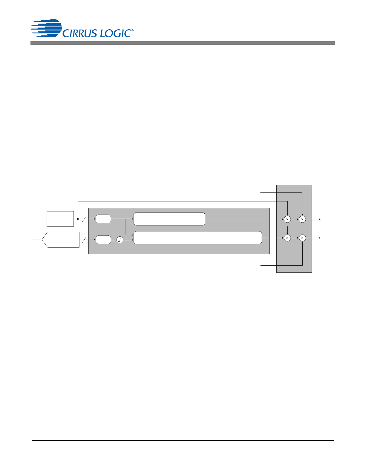
The CS1630/31 color control system has the ability to maintain a constant CCT or change
CCT as the light dims. OTP configurations allow the selection of the dimming profile. A
specific CCT profile can be programmed to the digital mapping device. The mapping is
two-dimensional: one current versus temperature profile is generated for each dim level.
The CS1630/31 provides two-dimensional mapping for the color LED’s current only, and
one-dimensional mapping (current versus dim level) for the other string.
The dim-regulated gain and dim-regulated plus temperature-regulated gain
AN374REV2 5
Page 6
AN374
dim
NTC
(From Boost)
12
8
÷ 4096
÷ 256
D
T
Normalize
Normalize
Saturation
Logic
GAIN
DR
= Q3 × D3 + Q2 × D2 + Q1 × D + Q0
GAIN
DTR
= P30 × T3 + P20 × T2 + P10 × T + P03 × D3 + P02 × D2 + P01 × D +
P21 × T
2
× D + P12 × T × D2 + P11 × T × D + P00
I
White(ref)
I
Red(ref)
I
White
I
Red
dim
dim
Temperature
(ADC Fast Filter)
Figure 1. Color Control System
GAIN
DTR
P30 T3 P20 T2 P10++T P03 D3 P02++D2 P01 D P21 T2D++= P12 T D2 P11 T D P00+++
GAIN
DR
Q3= D3 Q2 D2 Q1 D Q0+++
[Eq. 1]
3 Introduction to the Color System
The CS1630/31 is a two-channel TRIAC dimmable LED driver IC designed to change the color temperature of the
light output by independently varying the gains of the two different color LED strings to establish levels of color mixing. This feature can be used to make the color temperature versus dim characteristics of the light similar to that of
an incandescent light bulb. In many such designs, one of the LED strings is composed of red or amber LEDs, and
the other string is composed of cool-white or blue-white LEDs. While the lumen output of white LEDs does not vary
significantly across temperature, the lumen output of red LEDs can vary as much as 40% across temperature. To
achieve a consistent light output across temperature, the current in the red LED string needs to be compensated
with respect to temperature. Depending on the design, either channel can be temperature compensated.
Cirrus Logic, Inc. and its affiliates and subsidiaries generally make no representations or warranties that the combination of Cirrus Logic’s products with light-emitting diodes (“LEDs”), converter materials, and/or other components
will not infringe any third-party patents, including any patents related to color mixing in LED lighting applications,
such as, for example, U.S. Patent No. 7,213,940 and related patents of Cree, Inc. For more information, please see
Cirrus Logic’s Terms and Conditions of Sale, or contact a Cirrus Logic sales representative.
Figure 1 illustrates the block diagram of the color control block inside of the CS1630. The color temperature of the
light engine can be modified by changing the gains of each channel based on the current dim level. On the temperature-controlled channel, the currents can be varied according to the temperature sensed by an external NTC.
The required gain value for a particular combination of dim and temperature is obtained using polynomial curves,
the coefficients of which are programmed into the CS1630/31 OTP memory. A different polynomial is used for each
channel. One of these is a polynomial in two variables, dim and temperature, while the other is a polynomial in dim
only. If D and T are assumed to be the normalized dim and temperature values, respectively, between 0 and 1.0,
then GAIN
refers to the dim-regulated gain and temperature-regulated gain, and GAINDR refers to the dim-reg-
DTR
ulated gain.
As shown in Equation 1, the gain equation for the white is a third-order polynomial in dim, and the gain equation for
the red is a third-order polynomial in both dim and temperature. The color gain is third order to provide good tradeoffs
between computational overhead and being able to operate over the largest variety of LEDs across a wide range of
temperature. A lower-order polynomial fit, such as a quadratic or a linear fit, would not allow a large range of gain
values across the entire operating range. This would limit the sample space of available LEDs, since the gain is an
indirect reflection of its variation across temperature and required dim. As a result, a third-order fit allows the system
engineer to achieve a large variation in CCT and lumens across dim.
6 AN374REV2
Page 7

AN374
I
RedIRed ref
dim GAIN
DTR
=
[Eq. 2]
I
WhiteIWhite ref
dim GAIN
DR
=
[Eq. 3]
4 Light Engine Choices
This section examines key design considerations for a complete lamp design using the CS1630/31 two-channel
TRIAC dimmable driver IC. It provides some of the appropriate design choices based on a comprehensive
understanding of the CS1630/31 driver and digital control algorithms.
4.1 Considerations for the Color System
Constraint 1: Translating current versus dim requirements into a fourth-order or lower polynomial
Numerous smooth curves that do not have asymptotes at the origin can be modeled as a polynomial function.
The few exceptions are notable functions where the output current equals log
converter design requires a light engine that has a color curve that trends to any of these functions, then some
design tradeoffs must be considered. Such output current profiles are not widely prevalent in the consumer or
commercial lighting applications in which two-channel LEDs are typically used.
Constraint 2: The current versus dim plot should have intercept at origin
The final output currents for red current I
and white current I
Red
are calculated using Equations 2 and 3:
White
(dim) or 1/dim. If the power
10
These equations show that the current versus the dim will tend to the origin even for non-zero coefficients P00
and Q0.
The dim axis is an imaginary axis with no physical significance to an LED designer. This constraint causes
problems that can be substantially mitigated by remapping the dim axis, as demonstrated in section
Manipulating Data for Better Curve Fit on page 27.
Constraint 3: Placement of NTC with respect to light engine
The NTC can be placed close to the LEDs when the LEDs represent the junction temperature of the LEDs or
it can be placed farther away from the LEDs, where it represents the heat sink temperature or even the ambient
temperature inside the bulb. Each placement comes with its own advantages, and Steps 1 and 2 below
describe the implications of placing the LEDs in either location.
Step 1) Advantages of placing the NTC close to the LEDs
1. The problem of thermal mass is greatly reduced, which allows using simpler temperature protection and
thermal fold back.
2. Since the NTC is a good representation of the junction temperature, it is simpler to make light-system
models that can be used for designing the light engine.
3. Temperature protection systems such as thermal fold back and thermal shutdown can be more accurately
designed if needed, improving reliability in such applications.
Step 2) Disadvantages of placing the NTC close to the LEDs
1. The
of the NTC varies across temperature, and a narrow temperature range produces a more accurate
linear approximation. By having a large temperature rise on the NTC, the NTC is no longer accurate, since
the CS1630/31 can only accept a single
value and a single expression for the temperature.
2. If the thermal impedance between the NTC and the LED junction is large, the NTC will not accurately
represent the LED junction temperature, and the red current I
compensation may be incorrect. For
Red
example, when the NTC is placed close to the LED strings, then the measured temperature is a close
representation of the LED junction temperature. In a tight form factor and at full brightness, the
temperature rise from ambient to thermal equilibrium is significant. Typically, LED strings can take up to a
few minutes before they reach thermal equilibrium. When the system is started at ambient temperature
T
= 25C and full brightness, the NTC temperature and the junction temperature of the LEDs are at
amb
25
C. Since the curve fitter produces a gain function that is dependent on a combination of the red current
AN374REV2 7
Page 8

AN374
I
PK1 FBVBST
T1
CH1
L
P
----------------
200V
5.3s
3543H
---------------------
299m A== =
[Eq. 4]
I
MODE1 avgIPK1 FB
N
T2
CH1
2TT
----------------
299m
A 5.57
9.0s
2 35.05s
------------------------------
214m A== =
[Eq. 5]
I
, NTC, and dim variables, the curve fitter will have to compute gains across a larger number of points,
Red
which creates the risk of increased error. Failure to compensate for these points may cause a color shift
during startup until the LED strings reach thermal equilibrium.
Constraint 4: Red currents increase with an increase in ambient temperature
The current I
value.
in the red channel should increase monotonically with ambient temperature at a given dim
Red
Ambient Temperature
0
C300mA
25
C330mA
50
C360mA
Red Current Flowing in
Current Compensated Channel
Table 1. Maximum Measurable Switching Period
For example, if the current at ambient temperature T
T
= 25C, then the currents are non-monotonic with ambient temperature.
amb
= 50C is less than the current at ambient temperature
amb
Constraint 5: Maximum allowable color gain is 4.0
The recommended maximum gain value that the color system generates is 4.0. For example, the red current
at 25
C cannot be four times larger or smaller than any other current at the same dim value.
4.2 Constraints Imposed by Second Stage
Constraints in this section are imposed by the second stage. Calculations of these parameters are detailed in
application note AN368 Design Guide for a CS1630/31 2-Channel TRIAC Dimmable SSL Circuit. All variables
referenced in this document are computed in application note AN368.
Constraint 1: Currents in either channel should not be zero at non-zero dim values
Calculate peak current I
PK1(FB)
during Mode 1 using Equation 4:
Calculate the average current I
MODE1(avg)
during Mode 1 using Equation 5:
Equations 4 and 5 show that both channel currents share the same peak currents. It is difficult to have zero
current in one channel and have a non-zero current in the other channel. As a result, currents must be greater
than zero at all non-zero dim values.
Constraint 2: No abrupt change in current ratios at a dim point
It is recommended to avoid any abrupt change in the ratio of two-channel currents because it may cause color
flicker. The ratio of the channel current and the actual value of the string current should be a smooth function
which does not have any abrupt changes that become visible.
8 AN374REV2
Page 9

AN374
I
PK1 FB
I
PK2 FB
-------------------
P
MODE1
P
MODE2
--------------------=
[Eq. 6]
Constraint 3: Ratio of peak currents between the two channels must be less than 4
The DAC reference on the current sense comparator has a 1.4V full-scale threshold. There is a minimum peak
current I
ratio of the peak currents is 5.6. However, a range is required to dim down to the lower dimming settings.
Hence a ratio of 1.5 is considered optimum. Any peak ratio beyond 2.5 is considered a difficult requirement for
the driver to guarantee regulation across the dimming range. If the resonant reset time T3 is short and can be
neglected, then the ratio of the peak currents can be given as follows:
Refer to application note AN368 for detailed calculation.
Constraint 4: Both strings cannot have identical configuration
Either the output voltage differential should be maintained, or the output current differential should be
maintained. If the strings are placed in series, then the currents should never be the same at any point of the
dimming curve. If the strings are placed in parallel, then the voltage cannot be the same. The currents can
cross in a parallel load configuration. In a commercial lighting space that requires mixing white LEDs of
different wavelengths to produce a higher CCT white light (>3000K), it is recommended to have a different
number of white LEDs in the two LED strings when using the CS1630/31.
Constraint 5: Maximum differential between string voltages
The overvoltage protection (OVP) threshold is set to 1.25V and the FBSENSE comparator threshold is set at
a 200mV. As the dimmer conduction angle is reduced, the flyback operates continuously in DCM, while
maintaining valley switching for low losses. At very low conduction angles, the flyback may switch on the third
valley. Therefore, a minimum signal of 400mV on the FBAUX pin is recommended, which means that the string
voltage of one channel cannot be greater than three times the string voltage of the other channel in a parallel
load configuration. The FBAUX pin is used exclusively for overvoltage protection. In the event that a higher
string voltage differential is desired, an external circuit must be designed such that different divider ratios are
chosen for both modes of operation.
The OVP point is fixed for the higher of the two strings. For example, if one string has an output voltage of 5V
and the other string has an output voltage of 15V, the OVP point is still considered to be at greater than 15V.
Therefore, both output capacitors must be rated for the OVP voltage, which is in this case greater than 15V.
at full brightness threshold that is usually set at approximately 25%, so the theoretical maximum
PK(FB)
Constraint 6: The implications when determining LED string configuration and topology
Identify the light engine and select an appropriate second stage topology. There are two aspects that need to
be considered: first, whether to use the series or parallel LED configuration and second, which power train
topology to use.
AN374REV2 9
Page 10
AN374
Figure 2a. Flyback Series Output Model Figure 2b. Flyback Parallel Output Model
D2
R22
Z3
R21
R23
Q5
CS1630 /31
FBAUX
GND
13
GD
FBSEN SE
15
12
11
TX1
V
BST
R3
D6
U2
C10
C8
C15
D5
D
GND
_
Q
VCC
D15
R12 D10
Q3
R2
C16
Channel 1 LED
(White)
Channel 2 LED
(Red)
GND
IGND
I
MODEx
I
PRI
V
MODEx
D9
D2
R22
Z2
R21
R23
Q5
CS1630 /31
FBAUX
GND
13
GD
FBSEN SE
15
12
11
TX1
V
BST
R3
D6
U2
C10
C15
C8
D5
D
GND
_
Q
VCC
D15
R12 D10
Q3
R2
C16
Channel 1 LED
(Whi te )
Channel 2 LED
(Red)
GND
IGND
D9
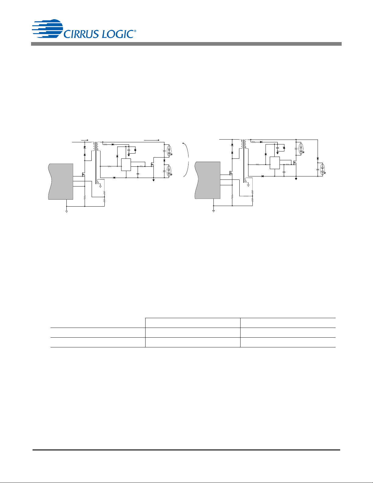
Step 1) LED string configuration
Determine if a series configuration or a parallel configuration is a viable solution for the identified light engine.
Figure 2a illustrates a series light configuration. The two LED strings are arranged in series so that current
passes through either one or both LED strings. A MOSFET is used to shunt current around one string on
alternating switching cycles. In this configuration, one string is required to have a larger current than the other
string. When considering a series design, it is recommended that the current flowing through one of the LED
channels be 80% or lower than that of the other LED channel at all times. The LED string that has current
flowing continuously is referred to as channel 1 LED (I
as channel 2 LED (I
CH2
); I
CH2
0.8I
CH1
.
), while the string with the bypass FET is referred to
CH1
Figure 2b illustrates a parallel light configuration. The two LED strings are networked in parallel so that current
flows to either the channel 1 LED string or the channel 2 LED string at any given T2 time. The CS1630/31
controller uses the LED forward voltage to detect which LED string is being driven. One LED string must
always have a larger forward voltage compared to the other LED string. The LED string with the higher voltage
is referred to as channel 1 LED with forward voltage V
to as channel 2 LED with a forward voltage of V
CH2
and the LED string with the lower voltage is referred
CH1
.
A good rule of thumb is that channel 2 LED must always have a forward voltage of 85% or lower than the
channel 1 LED to consider a parallel design. Table 2 defines the selection process based on the requirements
of the series and parallel output configuration.
V
< V
I
CH1
I
CH2
and I
CH2
< I
CH1
Cross Parallel Configuration Not Functional
CH2
Series or Parallel Configuration Series Configuration
CH1
Table 2. Series vs. Parallel
If there are problems converging on a target design using an existing light engine, the current and voltage
profile can be modified by adding, removing, or moving LEDs between the two LED channels. Figure 3
illustrates the parallel and series scenarios that can be configured using the CS163X Customer Application
tool.
10 AN374REV2
V
CH1
and V
CH2
Cross
Page 11
AN374
Step 2a:
Select Series
vs. Parallel
Step 2b:
Select Flyback,
Buck, or
Tapped Buck
Figure 3. Second Stage String Configuration
Bit STRING in register Config3 at address 7 selects the second stage output channel configuration. When bit
STRING is set to ‘1’ a series configuration is selected. Figure 3 illustrates the process used to select the
second stage flyback mode using the CS163X system design application.
Step 2) Select power train topology
The CS1630/31 supports three possible power train configurations: tapped buck, buck, and flyback (see
Figure 4a, 4b, and 4c). The two most important factors for selecting a power train configuration is whether the
output requires Underwriters Laboratory (UL) approved isolation and the input to output voltage ratio. The
flyback power train can be either isolated or non-isolated. Buck and tapped-buck designs are expected to
always be non-isolated. If isolation is not required, one of the three possible solutions must be selected. If
isolation is required, the design will be a flyback.
AN374REV2 11
Page 12

AN374
Figure 4a. Tapped Buck Series Output Model Figure 4b. Buck Series Output Model
R22
R21
R23
Q5
L3
D3
CS1630 /31
FBAUX
GND
13
GD
FBSENSE
15
12
11
V
BST
R3
D9
U2
C10
C8
C15
D11
D
GND
_
Q
VCC
R12 D10
Q3
R2
C14
Channel 1 LED
(White)
Channel 2 LED
(Red)
GND
IGND
D9
R22
R21
R23
Q4
L3
CS1630 /31
FBAUX
GND
13
GD
FBSENSE
15
12
11
D3
V
BST
R25
D9
U2
C13
C15
C16
D11
D
GND
_
Q
VCC
R26 D10
Q5
R27
C14
Z3
Channel 1 LED
(Whi te )
Channel 2 LED
(Red)
GND
IGND
Figure 4c. Flyback Series Output Model
D2
R22
Z3
R21
R23
Q5
CS1630 /31
FBAUX
GND
13
GD
FBSENSE
15
12
11
TX1
V
BST
R3
D6
U2
C10
C8
C15
D5
D
GND
_
Q
VCC
D15
R12 D10
Q3
R2
C16
Channel 1 LED
(White)
Channel 2 LED
(Red)
GND
IGND
I
MODEx
I
PRI
V
MODE x
D9
Flyback topology is enabled by setting bit S2CONFIG to ‘1’ in register Config12 at address 44. A flyback
topology is selected as a design guide example in application note AN368 so bit S2CONFIG is set to ‘1’. The
flyback transformer input-to-output voltage ratio is used to determine the duty cycle and minimum turn on time
T1 for the power FET. Buck topology is enabled by setting bit S2CONFIG to ‘0’ in register Config12 at address
44. If a buck topology is selected, the buck inductor is configured using bits BUCK[3:0] in register Config10 at
address 42. Set bits BUCK[3:0] to ‘0’ or ‘1’ for a normal buck topology. Tapped buck topology is enabled by
setting bit S2CONFIG to ‘0’ in register Config12 at address 44 and by setting bits BUCK[3:0] in register
Config10 at address 42 to the required value N, where N equals the turns ratio between primary and secondary
windings.
12 AN374REV2
Page 13

AN374
Figure 5. Selecting the Second Stage Mode Using the CS1630/ 31 System Design Utility
P
MODE1
V
CH1VCH2
+I
CH2
=
[Eq. 7]
Figure 5 illustrates the process used to select the second stage flyback mode using the CS1630 / 31 system
design utility.
The CS1630/31 has a minimum required T1 time that is dependent on leading edge blanking time T
Blanking time T
is programmable from 150ns to 800 ns and is used to effectively disable the peak current
LEB
comparator from turning off the gate drive too early due to spurious switching noise. In applied systems, a good
rule of thumb is to target a minimum duty cycle of 10% or greater.
Step 3) General considerations for all topology
1. In the series configurations, the current in one string will always be higher than the current in the second
string across the entire dim and temperature range. There are specific advantages to using the series configuration if the light engine specifications comply with the constraints. In Mode 1, the phase synchronizer
MOSFET is ‘OFF’ and the output power P
delivered to the load in a series design is calculated using
MODE1
Equation 7:
AN374REV2 13
LEB
.
Page 14

AN374
P
MODE2
I
CH1ICH2
–V
CH1
=
[Eq. 8]
P
MODE1
V
CH1ICH1
=
[Eq. 9]
P
MODE2
V
CH1ICH2
=
[Eq. 10]
In Mode 2 the phase synchronizer MOSFET is turned ‘ON’ and the output power P
MODE2
is:
2. In the parallel configuration, the voltages of the two strings should at least have a 20% difference between
the two strings in order for the CS1630/31 to distinguish between the two strings. The most common
application of a parallel string is to achieve low CCT at low dim (<2000 K) and maintain ~ 2700 K at full
brightness using a combination of mint/blue/white on one channel and amber/red on the other channel.
Depending on the configuration, the current I
in the white channel at low dim, whereas the current I
brightness. When the phase synchronizer MOSFET is ‘OFF’ the output power P
in the red channel may be higher than the current I
Red
may be higher than current I
White
MODE1
delivered to the
Red
White
at full
load in a parallel design is as follows:
and when the phase synchronizer MOSFET is turned ‘ON’ the output power P
MODE2
is as follows:
3. If the power delivered to the load is similar in both configurations, then the magnetic utilization will be the
maximum and the inductor size will be the smallest. For an LED configuration, the power can be computed
in the four possible scenarios and it can be determined which design would be the optimum if the size of
the inductor were the dominant factor in deciding between series and parallel configurations.
4. To quantify magnetic size, consider analyzing the peak current I
inductance L
of a system designed to drive a single LED string. For example, examine a design with the
P
, turns ratio N, and primary
PK(FB)
single string CS1610/11/12/13 driver IC. For a comparable CS1630/31-based system converting the same
level of output power, let peak current I
be I
PK2(FB)
. It is assumed that I
PK1(FB)
for Mode 1 be I
PK(FB)
> I
PK2(FB)
PK1(FB)
and peak current I
PK(FB)
for Mode 2
. Let turns ratio N be such that the effective reflected
voltage be the same so that their peak currents would be comparable between the two systems under
comparison.
14 AN374REV2
Page 15

AN374
Pow er Transf erred in a S ingle S tring Cont roller
Pow er Transf erred in a Tw o String C ontrol ler with
Unequal Balanc e between Two S trings
t
i(t)
T1 T2
TT
T3T1 T2
TT
T3
TT
T1
CH1
T2
CH1
TT
CH1
T3
CH1
T1
CH2
T2
CH2
TT
CH2
T3
CH2
t
Figure 6. Current Comparison through the Inductor
P
OUT dualPMODE1PMODE2
+= 2P
OUT glesin
[Eq. 11]
P
MODE1
P
OUT glesin
-----------------------------
2
1 +
------------------
[Eq. 12]
2F
sw
1 +F
sw1
------------------------------------
[Eq. 13]
Figure 6 illustrates the current comparison through the inductor. In this case, the buck is chosen to explain
the point. The same logic can be extended to the flyback topology as well.
In a single-string design, power P
OUT(single)
ered in the second switching period and the total power is equal to two times power P
channel design, the total power P
OUT(dual)
delivered in the first switching period TT equals power deliv-
OUT(single)
. In a two-
is approximately equal to:
The above equation yields Equation 12:
where
= P
MODE2/PMODE1
The size of the inductor depends on the amount of energy stored at a first-order approximation. The energy
stored in the inductor of a single string system is equal to P
in the inductor of a two string system is equal to P
by:
From Equation 13, it can be seen that the inductor for a CS1630/31-based equivalent system will be
Fsw. The maximum energy stored
. The size factor of the inductor is defined
MODE1
OUT(single)
F
sw1
times larger.
AN374REV2 15
Page 16

AN374
F
SW2
F
SW1
V
BST
NV
MODE1
+
V
BST
NV
MODE2
+
----------------------------------------------------------
I
MODE1VMODE2
I
MODE2VMODE1
------------------------------------------
=
[Eq. 14]
The following are disclaimers for this analysis:
a. This analysis works better for a non-isolated design. For isolated flyback designs, the size may be deter-
mined by safety requirements for either triple insulated wire or margin tape spacing. As a result,
increased peak current may or may not translate into the size of the inductor easily.
b. The explanation above shows a qualitative trend in understanding the tradeoffs of having power deliv-
ered to two strings unevenly. It is understood that it is not possible to determine a true analogy since the
reflected voltage and frequency vary over the two modes of operation in the CS1630/31. This comparison should only be viewed from a qualitative understanding of the system.
5. When considering efficiency, if the power delivered to the load in the two modes is significantly different,
then the frequency of operation of switching frequency F
the converter operates in CRM at full brightness.
The converter will switch at a very high frequency while converting very little power. The power converter’s
efficiency is low, however the power is transferred at two different frequencies and some amount of
spreading effects of the spectral energy can be observed. This can potentially be favorable from an EMI
perspective.
Step 4) Analyze system tradeoffs for efficiency when using a flyback topology
In a parallel configuration, the turns ratio will be higher for a given reflected voltage, so the leakage inductance
will also be higher. As a result, the peak voltage on the drain of the flyback MOSFET must be taken into
account. Since the effective output voltage is smaller, the synchronizer diode drop amounts to a much bigger
efficiency penalty as opposed to the parallel design case.
In a series design, the leakage inductance will be smaller for the same reflected voltage. The maximum voltage
on the rectifier diode is given by V
/ N + V
IN
. The diode must be a higher voltage rated diode, which
OVP
increases cost and may impact efficiency, depending on the reflected voltage.
In a flyback topology, it is difficult to predict the diode losses prior to the development of a system, since diode
losses vary significantly with junction temperature. This step is meant to serve as an added consideration when
choosing a certain load configuration.
sw1
and F
will be significantly different because
sw2
Step 5) Analyze system tradeoffs for efficiency when using a buck topology
The minimum voltage rating for the power diode is greater than 250V for the CS1630 and greater than 450V
for the CS1631. In order to guarantee optimum output current regulation in a buck converter, it is desirable to
have a duty cycle of at least 10%, and any duty cycle above 15% is considered optimal for the buck converter.
In a parallel configuration, the effective output voltage is lower, and the diode losses higher. The duty cycle is
smaller, since the effective output voltage is smaller. In a series configuration, the diode losses are lower, since
the diode drop is still set by the boost voltage V
and not the output voltage.
BST
Constraint 7: Note on Frequency and EMI
The frequency of the double pulse is dependent on the ratio of the power delivered in each mode. Both strings
having different power levels provides natural spreading of the spectrum for EMI. However, it decreases the
magnetic utilization of the core.
The following are the hard constraints on the frequency of operation:
1. Maximum switching frequency cannot exceed 200kHz.
2. Minimum switching frequency cannot be lower than the value programmed in the OTP register TTMAX at
Address 38.
16 AN374REV2
Page 17

AN374
R22
R21
R23
Q4
L3
CS1630 /31
FBAUX
GND
13
GD
FBSEN SE
15
12
11
D3
V
BST
C16
C15
D11
R27
Channel 1 LED
(Wh ite )
Channel 2 LED
(Red)
GND
R25
Q6
R26
SYNC
Q5
GND
Figure 7. Non-isolated Synchronizer Buck Series Output Model
4.3 Synchronizer Design Considerations
The synchronizer circuit drives an external MOSFET, which may be ground referenced depending on the topology.
Constraint 1: Non-isolated synchronizer circuit considerations
In the case of a non-isolated flyback, the secondary ground of the flyback can be referenced to the primary
ground thereby having the least expensive synchronous circuit solution consisting of the synchronous
MOSFET and the diode. The MOSFET is directly driven from the SYNC pin of the CS1630/31.
In the case of the buck topology, the outputs are referenced to link voltage and the following two options are
possible:
1. Level shifting the SYNC pin output to a higher voltage using an external BJT and a P-channel MOSFET
(see Figure 7).
2. Driving the synchronizer externally using flip-flop from the switching node or another winding off of the
buck converter.
4.4 Constraints on the Boost Stage
Constraint 1: Maximum power should be power at full AC sine wave
It is recommended to design the dimming curve such that the maximum output power is delivered to the load
at 100% brightness when the driver is behind the full AC sine wave.
Constraint 2: Power should be monotonically increasing
The output power in the driver should be close to monotonically increasing. If the available power from the
dimmer cut waveform at any conduction angle is smaller than the requested output power, then the link voltage
may not be in regulation at that conduction angle. In such a case, the peak currents on the boost inductor need
to be increased, and all design calculations mentioned in application note AN368 are no longer valid for that
particular design. Increasing peak currents may compromise EMI and efficiency.
AN374REV2 17
Page 18

5 Design Flowchart
Yes
No
Yes
No
Yes
No
Pick a light engine
candidate across dim
Compute peak currents
for a given transformer
using AN368
Start
Polynomial
approximation
possible?
Non-zero
currents across
dim?
Peak
current 4 times
smaller?
Proceed to choosing
string configuration
No abrupt
change in
current
ratio
?
Nonidentical string
configurations
across
dim?
Yes
Yes
No
No
No fundamental
limitations to using
light engine?
Figure 8. Eliminating Incompatible Light Engines
Figure 8 shows the flowchart for eliminating incompatible light engines.
AN374
18 AN374REV2
Page 19

Figure 9 shows a way for selecting the correct second stage string configuration.
Yes
No
Yes
No
Yes
No
Provide completed light
engine design across
dim and temperature
Not compatible
No hard limitations to
using either
string configuration
Start
Parallel string
configuration
Series string
configuration
Currents
cross at
any dim?
Voltage
Same?
Voltage
same?
Yes
No
Flyback topology. Series
and parallel string
configurations are sufficient
Buck?
Proceed to selecting
the topology
The series string
configuration has
higher efficiency
Figure 9. Selecting the Correct Second Stage String Configuration
AN374
AN374REV2 19
Page 20

Figure 10 shows a method for selecting the correct power train topology.
No
Yes
No
Start
Flyback
Flyback
Buck
Isolation
required?
Required
V
MODEx
/ V
BST
< 10%
Yes
Figure 10. Selecting the Correct Power Train Topology
AN374
20 AN374REV2
Page 21

AN374
1600
650
1
2
3
2700
Brightness (lm)
CCT (K)
Figure 11. Typical LED Light Engine Specifications
0.02
650
Brightness (lm)
1.0
1
0.02
2700
1600
CCT (K)
Dim
1.0
2
3
Figure 12. Light Engine Specifications Translated to an Imaginary Dim Axis
6 Data Improvements for the Curve Fitting Process
The curve-fitting process consists of translating a typical LED system specification into polynomial gain equations
that the curve fitter can then calculate the required current for a given dim and NTC reading. The gains can be used
in conjunction with the design of the power stage to complete a system design for a CS1630/31-based LED driver.
6.1 Typical Light Engine System Specifications
A typical light engine system specification is concisely captured in Figure 11. It is essentially a plot of the target
lumen output at a given target color correlated temperature (CCT). Points 1, 2, and 3 are some data points of
interest. These points have been used to define system behavior. The graph shows that the behavior is
expected to be constant across the entire operating temperature of the driver. If the behavior over temperature
were different, it can be represented as separate parameterized curves using the same axis.
6.2 Translation into Input Specifications for Calculating Color Gains
The light engine specifications above need to be translated into typical driver specifications that can be used
by the second stage of the CS1630/31 based driver.
Step 1) Introduction of an independent dim axis
The curve fitter polynomial equation is an equation across dim and NTC temperature. The independent dim
axis can be introduced as shown in Figure 12. At this point, the specifications can be redefined as needed to
find a trajectory the light engine needs to traverse in terms of CCT and brightness when the input dim level to
the system changes.
AN374REV2 21
Page 22

Step 2) Translate into LED current profile at room temperature
m1, I
Red
, m2, I
White
I
Red
/ I
White
Ratio of the 2
Channel’s Lumens
Sum of Each
Channel’s Lumens
Approximated
Using Current
Approximated
Using Current
0.02
650
1.0
1
0.02
2700
1600
Dim Dim Dim
1.0
2
3
0.02 1.0
1
0.02
Ratio
1.0
2
3
0.02 1.0
1
0.02
Ratio
1.0
2
3
K
1
, P
Red
+ K2, P
White
K1, P
Red
K
2
, P
White
Brightness (lm)
Brightness (lm)
Relative Brightness (lm)
CCT (K)
Figure 13. Translate Data and CCT Lumen Dependence on Output Current
0.02
Red
1.0
T
amb
= 5°C
T
amb
= 25°C
T
amb
= 40°C
T
amb
= 55°C
Figure 14. Red Current Across Dim at Various Ambient Temperatures
The translation is as shown in Figure 13.
AN374
Variables K
and K2 represent the luminous efficacy of the LED, and variables m1 and m2 are arbitrary
1
constants. The plot in Figure 13 illustrates the relationship between CCT and output currents, lumens, and
output power.
The data points 1, 2, and 3 are recreated under thermal equilibrium with the target LED light engine at room
temperature to obtain the LED current profiles for each channel across the entire range of the target lumen
output. The NTC temperature recorded on the final measurement is used on the driver. At the end of this
procedure, the following are obtained: the current versus dim, forward voltage versus dim, NTC resistance
versus dim, current ratio versus dim, and the LED light engine power profile data at room temperature.
Step 3) Validate data across various ambient temperatures
Finally, the same step needs to be completed across different ambient temperatures. All the measurements
should be performed when the system has reached thermal equilibrium. Once the data is taken, the sample
data is shown in Figures 14 and 15.
(A)
I
Dim
22 AN374REV2
Page 23

Note that any variation of the white string should be compensated for by changing the currents in the other
0.02 1.0
Dim
T
amb
= 5°C
T
amb
= 25°C
T
amb
= 40°C
T
amb
= 55°C
NTC Resistance (:
Figure 15. NTC Codes Across Dim at Various Ambient Temperatures
string so that the correct lumen and CCT are maintained across the entire temperature range of interest. At
this point, both the currents of the white LED across dim and the data represented in Figures 14 and 15 should
be available for the design.
6.3 Methods to Collect Required Data
The following sections describe the methods to collect the necessary data required for performing curve fitting.
6.3.1 Experimental Measurement in Lab
Experimental measurements are the most robust way to collect data. However, it is time consuming and
requires expensive test equipment. It also requires the final light engine that is to be used for the design. The
thermal resistance between the LED junction and the NTC should be known. In other words, the NTC should
be placed at its final location to best mimic the thermal resistance. The light engine should be placed in an
integrating sphere and characterized. For example, specifications with regards to CCT, Cx, Cy, lumens, and
CRI can be measured.
Each output string is connected to an independent DC source that can source the required voltage and
currents. The currents are experimentally changed until the desired points 1, 2, and 3 are obtained on
Figure 11. At each of these points, measure the NTC resistance when it stabilizes to a constant value. If the
NTC is not placed, then a thermocouple can be placed close to where the NTC will be placed and the
temperature can be recorded.
The process should be repeated at various ambient temperatures. The entire data is collected across the
various ambient temperatures to cover the thermal operating point space of the LEDs, which it is forced to
traverse during transients (even though the actual ambient temperature is not what was specified in the
spreadsheet). For example, it can alleviate the color shift problem at cold startup, as discussed in
sectionTranslation into Input Specifications for Calculating Color Gains on page 21.
Another advantage of this approach is that it naturally compensates for any variation in the behavior of the
other string across the various ambient temperatures by adjusting the two strings accordingly. Performing this
experiment of accurately measuring the data across various ambient temperatures using an integrating sphere
is not easy.
AN374
6.3.2 Simulation
Some of the designs can be done on the spreadsheet if at the least the following are available:
• Theoretical models for LED behavior across junction temperature
• Thermal model of the junction to NTC temperature thermal resistance
• NTC model
• Good optics and reflector model with respect to diffuser and LED beam angles
AN374REV2 23
Page 24

AN374
T
amb
TJT
25 C
–=
[Eq. 15]
T
NTC
TJT
NTC
–=
[Eq. 16]
TJT
amb 0CTamb
+=
[Eq. 17]
T
NTC
T
amb 0CTNTC
+=
[Eq. 18]
R
T1
RT0e
1
T1
-------
1
T0
-------
–
=
[Eq. 19]
I
Red 0CIRed 25C
1
2
-------
=
[Eq. 20]
I
Red 40CIRed 25C
1
3
-------
=
[Eq. 21]
6.3.3 Experiment and Approximation
In many cases, collecting data at room ambient is not difficult. However, getting data across various ambient
temperatures, particularly at low temperatures, is not easy. In an event where getting data is not feasible at
ambient temperatures outside of room temperature, existing 25
based on data sheet numbers of the LED and measured temperature rises. If the requested operating
temperature is very large (
T
> 50C), then the errors due to this simple linear approximation may be too
amb
high. Remember that the method is a simple approximation and subject to errors that may vary depending on
the system under investigation.
The following method is suggested to extend data to other ambient temperatures. In this case, two ambient
temperatures of 0
C and 40C are chosen. These are some of the assumptions that are made. The
temperature rise from ambient is assumed to be constant irrespective of the actual ambient temperature level.
Step 1) Collect red current I
25
C ambient temperature T
, white current I
Red
amb(25C)
, and NTC data and junction temperature TJ of the LED at
White
from 0% dim to 100% dim.
Step 2) Calculate the following:
C data can be extended to other temperatures
Step 3) Calculate the various NTC temperature T
and junction temperature TJ of the LED at various
NTC
ambient temperatures across the entire dimming range as follows:
Step 4) Calculate the NTC resistance using the equation of the system at 25
C ambient and the expression
At this point, a complete sample space has been recreated using the temperature rise. The remaining steps
are focused on recreating the red currents I
across temperature.
Red
Step 5) Refer to the LED data sheet for the Relative Luminous Flux Curve and note the relative luminous flux
at ambient temperature T
fluxes at 25
C, 0C, and 40C ambient, then the red currents can be calculated using Equations 20
= 25C, 0C, and 40C. If 1, 2, and
amb
are the relative luminous
3
and 21:
Thus by performing this at every dim level, the entire dimming data required can be constructed.
24 AN374REV2
Page 25

6.4 Improving Data for Feeding the Curve Fitter
NTC Beta 4334 Vref 1.25 ENTER DIM VALUES (BwDim, RedDim), CURRENTS (I_bw, I_red)AND NTC TEMPERATURE (Tntc) in deg. C
NTC T0 °C 25 Nbit 8 NTC code IS COMPUTED FROM Tntc AND NTC PARAMETERS
NTC Rs at T0 100000 Ifs 8.00E-05
Series R 14000 іNTC PARAMETERS
љљ
BwDim I_bw (A) ї enter 0.1 0.2 0.3 0.4 0.5 0.6 0.7 0.8 0.9 1 0.1 0.2 0.3 0.4 0.5 0.6 0.7 0.8 0.9 1
0.1 0.068
0.2 0.131 Tamb(room)
computedќ
enter ќ
0.3 0.190 ї enter 5.00 0.042 0.078 0.110 0.138 0.161 0.180 0.196 0.207 0.216 0.221 0.09 0.16 0.23 0.28 0.33 0.37 0.40 0.42 0.44 0.45
0.4 0.246 15.00 0.044 0.083 0.116 0.145 0.170 0.190 0.206 0.218 0.227 0.233 0.09 0.17 0.24 0.30 0.35 0.39 0.42 0.45 0.46 0.48
0.5 0.297 25.00 0.046 0.087 0.122 0.153 0.179 0.200 0.217 0.230 0.239 0.245 0.09 0
.18 0.25 0.31 0.36 0.41 0.44 0.47 0.49 0.50
0.6 0.344 45.00 0.049 0.091 0.128 0.160 0.187 0.210 0.228 0.241 0.251 0.257 0.10 0.19 0.26 0.33 0.38 0.43 0.46 0.49 0.51 0.53
0.7 0.386 65.00 0.051 0.096 0.135 0.168 0.197 0.220 0.239 0.253 0.264 0.270 0.10 0.20 0.28 0.34 0.40 0.45 0.49 0.52 0.54 0.55
0.8 0.425 85.00 0.053 0.101 0.142 0.177 0.207 0.231 0.251 0.266 0.277 0.284 0.11 0.21 0.29 0.36 0.42 0.47 0.51 0.54 0.57 0.58
10.490
Tamb(room) enter ќ
5.00 5.20 7.40 9.60 11.80 14.00 16.20 18.40 20.60 22.80 25.00
15.00 15.20 17.40 19.60 21.80 24.00 26.20 28.40 30.60 32.80 35.00
25.00 25.20 27.40 29.60 31.80 34.00 36.20 38.40 40.60 42.80 45.00
45.00 45.20 47.40 49.60 51.80 54.00 56.20 58.40 60.60 62.80 65.00
65.00 65.20 67.40 69.60 71.80 74.00 76.20 78.40 80.60 82.80 85.00
computedќ
13.5 15.2 17.0 19.0 21.2 23.6 26.1 28.9 31.9 35.1
22.5 25.0 27.6 30.5 33.6 36.9 40.5 44.2 48.2 52.4
35.4 38.8 42.5 46.3 50.4 54.7 59.2 64.0 68.9 73.9
74.4 79.7 85.1 90.6 96.2 102.0 107.7 113.6 119.5 125.3
Hight Temp Code Limit 185 125.9 131.7 137.5 143.3 149.0 154.6 160.0 165.4 170.7 175.8
Low Temp Code Limit 12 176.2 181.1 185.9 190.6 195.0 199.3 203.4 207.4 211.2 214.8
RedDim
RaƟo (String2/String1)
Tntc[C]
NTC code
I_red
0.00
0.10
0.20
0.30
0.40
0.50
0.60
0.70
0 0.2 0.4 0.6 0.8 1 1.2
RaƟo
Dim
Current RaƟos Vs Dim
Tamb = 5C
Tamb=15C
Tamb = 25C
Tamb=45C
Tamb=65C
Tamb=85C
0.000
0.100
0.200
0.300
0.400
0.500
0.600
0 0.2 0.4 0.6 0.8 1 1.2
Output Current (mA)
Dim
Currents Vs Dim
I_BW
I_RED 5C
I_RED 15C
I_RED 25C
I_RED 45C
I_RED 65C
I_RED 85C
Step 1:
Enter NTC
Configuration
Step 4:
Enter Current Ratio
vs Dim and Temp
Step 5:
Enter Temperature or
NTC Resistance
Step 6:
Compute NTC Code
Step 3:
Enter Red Current vs
Dim and Temperature
Step 2:
Enter Blue
Current vs Dim
Figure 16. Example Spreadsheet Used to Collect Curve Fitting Data
NTC Beta 4334 Vre f 1.25
NTC T0 °C 25 Nbit 8
NTC Rs at T0 100000 Ifs 8.00E-05
Se ries R 14000
Does Not Change
Figure 17. NTC Specification from Example Spreadsheet
NTC
CODE
4M
R
Series
RT0e
1
T1
-------
1
T0
-------
–
+
--------------------------------------------------------------------------
=
[Eq. 22]
This section demonstrates the use of a spreadsheet to manipulate the data collected in the previous section
to get a more accurate curve fit. The data is presented in a format compatible with the curve fitter software.
6.4.1 Understanding the Data and Data Format
The final data can be collected in a spreadsheet. An example of the spreadsheet is shown in Figure 16. Steps
are provided to the left to describe the process.
enter enter
0.9 0.460
85.00 85.20 87.40 89.60 91.80 94.00 96.20 98.40 100.60 102.80 105.00
AN374
The NTC configuration section is shown in Figure 17. Values for Vref, Nbit and Ifs are internal parameters of
the IC that do not change. The beta and initial resistance at the initial temperature can be changed.
The NTC code can be generated using Equation 22. If temperature is specified in the system, then:
where
Temperature T1 and T0 are in degrees Kelvin
AN374REV2 25
Page 26

AN374
NTC
4M
R
NTCRSeries
+
--------------------------------------
=
[Eq. 23]
enter enter
љљ
0.1 0.068
0.3 0.190
0.4 0.246
0.6 0.344
0.7 0.386
0.8 0.425
0.9 0.460
Enter dim values
in ascending order
At 50% dim,
I
White
= 0.297 A
Figure 18. Example of Formatted Data for the White/Blue Current Across Dim
ї enter 0.1 0.2 0.3 0.4 0.5 0.6 0.7 0.8 0.9 1
5.00 0.042 0.078 0.110 0.138 0.161 0.180 0.196 0.207 0.216 0.221
15.00 0.044 0.083 0.116 0.145 0.170 0.190 0.206 0.218 0.227 0.233
25.00 0.046 0.087 0.122 0.153 0.179 0.200 0.217 0.230 0.239 0.245
45.00 0.049 0.091 0.128 0.160 0.187 0.210 0.228 0.241 0.251 0.257
85.00 0.053 0.101 0.142 0.177 0.207 0.231 0.251 0.266 0.277 0.284
5.00 5.20 7.40 9.60 11.80 14.00 16.20 18.40 20.60 22.80 25.00
15.00 15.20 17.40 19.60 21.80 24.00 26.20 28.40 30.60 32.80 35.00
65.00 65.20 67.40 69.60 71.80 74.00 76.20 78.40 80.60 82.80 85.00
85.00 85.20 87.40 89.60 91.80 94.00 96.20 98.40 100.60 102.80 105.00
computedќ
13.5 15.2 17.0 19.0 21.2 23.6 26.1 28.9 31.9 35.1
22.5 25.0 27.6 30.5 33.6 36.9 40.5 44.2 48.2 5 2.4
125.9 131.7 137.5 143.3 149.0 154.6 160.0 165.4 170.7 175.8
176.2 181.1 185.9 190.6 195.0 199.3 203.4 207.4 211.2 214.8
RedDim
Tntc[C]
NTC code
I_red
At 30% dim,
I
Red
= 0.122 A and
T
NTC
= 29.60°C
Enter dim values in ascending order
Enter
temperature
values in
ascending
order
Figure 19. Example of Formatted Data for Red Current and NTC Resistance/Code Across Dim
If resistance is measured, then
The data below shows the white/blue currents across the dim. The format in Figure 18 is useful because it is
required when the data is imported into the curve fitter.
BwDim I_bw (A)
0.2 0.131
0.5 0.297
10.490
The blue/white current at 100% will be considered the nominal current at full sine wave. The reference currents
are set based on this value.
The red currents and the corresponding temperature data are shown below.
Tamb(room)
Tamb(room) enter ќ
The target currents will be the currents at 100% dim and 25
Figure 19 shows the computed NTC resistance according to Equation 22. The NTC code is the internal
computed value used by the CS1630/ 31.
26 AN374REV2
computedќ
65.00 0.051 0.096 0.135 0.168 0.197 0.220 0.239 0.253 0.264 0.270
25.00 25.20 27.40 29.60 31.80 34.00 36.20 38.40 40.60 42.80 45.00
45.00 45.20 47.40 49.60 51.80 54.00 56.20 58.40 60.60 62.80 65.00
35.4 38.8 42.5 46.3 50.4 54.7 59.2 64.0 68.9 73.9
74.4 79.7 85.1 90.6 96.2 102.0 107.7 113.6 119.5 125.3
C ambient temperature. The NTC code data in
Page 27

AN374
6.4.2 Manipulating Data for Better Curve Fit
As mentioned previously, the curve fitter looks for a polynomial fit with a maximum of fourth order. There are
a few quick techniques that can be performed to make a better fit. This section shows some of the common
techniques used to improve the quality of data and therefore the quality of the fit. In this section, it is assumed
that the data, if attempted to be fitted using a curve fitter, provides a large error, so improvements are
necessary.
Step 1) Use a weighted fit
A weighting inequality can be enforced such that some regions can be given higher weights thereby forcing
the curve fitter to reduce the error while fitting in those regions. This is particularly useful when the observed
error is skewed more towards the region of interest as opposed to regions where the light bulb may not operate
regularly.
Step 2) Identify the region of interest
Some data points on the curve fitter have a larger significance to the light bulb as opposed to others. These
regions should be identified immediately and the curve fitting should be done in such a way that the errors in
these regions are minimized as a first priority.
Consider an example where an incandescent dimming profile is requested with 2% lumen output is required
at the lowest dim settings. Since all the major standards and specifications such as UL, LM79 are based on
full sine wave operation, that region is important and high accuracy in both lumen output and CCT is desirable.
From experience, it has been observed that at a low conduction angle, the light output is so small that the eye
is not yet saturated and if the two strings are not mixed correctly along the Planckian locus, the individual
components will be visible. It is important for the curve-fitting process to have minimal error in this region. In
most of the other regions, some amount of allowance could possibly be made depending on the application.
Step 3) Add trendline in a spreadsheet to see outliers in data
The trendline function in a spreadsheet or any other function in a compatible software helps identify any
outliers in the data. The following guidelines describe what to consider while using this trendline functions:
1. Choose a polynomial function of order 2, 3, or 4 for the current versus dim on the red and white currents.
A linear fit is acceptable if it produces a lower mean squared error (MSE).
2. Set intercept to origin
3. Display the equation on the chart
4. Display MSE on the chart (R2)
5. The trendline provides physical intuition in understanding where the potential problems may lie in trying to
fit the data into a polynomial curve.
Step 4) Dim axis remapping
Many data that may even look fundamentally incompatible with the curve fitter can be made to fit well by
remapping the dim axis. Mathematically a straight line with an equation Y = Mx + B can be made to be a line
Y = Mx by adding -B/M to every point on the x axis. Thus by shifting the whole axis to the right by B/M, the
curve can be made to pass through the origin.
Figure 20 shows another example of the above statement. In this case, by merely changing the dim point on
the axis from 0.4 to 0.5, the data that was an outlier is now part of the good data set. From a physics standpoint,
this still does not have any impact to the system specifications since the red current and the white current
combination remain the same.
AN374REV2 27
Page 28

AN374
0.05
0.125
0.25
0.375
0.5
0.03
0.075
0.15
0.225
0.3
0
0.1
0.2
0.3
0.4
0.5
0.6
0 0.2 0.4 0.6 0.8 1 1.2
LED Current (A)
Red LED Current
White LED Current
Figure 20. White and Red LED Current vs Dim
Notes: 1. Based on relative brightness.
Dim
1
I
White
(mA) I
Red
(mA)
0.10 0.050 0.030
0.25 0.125 0.075
0.40 0.250 0.150
0.75 0.375 0.225
1.00 0.500 0.300
0.05
0.125
0.25
0.375
0.5
0.03
0.075
0.15
0.225
0.3
0
0.1
0.2
0.3
0.4
0.5
0.6
0 0.2 0.4 0.6 0.8 1 1.2
Current (A)
White LED Current
Red LED Current
Figure 21. Corrected White and Red LED Current vs Dim
Notes: 1. Based on relative brightness.
Dim
1
I
White
(mA) I
Red
(mA)
0.10 0.050 0.030
0.25 0.125 0.075
0.50 0.250 0.150
0.75 0.375 0.225
1.00 0.500 0.300
When re-mapping the dim axis, remember the following points:
• The dim axis needs to be remapped to the white current and the red current axis simultaneously.
Otherwise, the data will be altered.
• In the plot in Figure 20 it can be seen that the data point is to the left of the trendline for the red current and
the white current. Moving the dim axis helps mitigate the problem under these circumstances.
Dim (%)
• If the red point and the white point were tending in the opposite way, remapping the dim axis to the center
could split the error for the same polynomial. One can change the shape of the trendline used for either one
of the curves by changing its order and then again attempting to remap the dim axis to see if a better fit can
be achieved.
28 AN374REV2
Step 5) Eliminating points outside the region of interest
If remapping the dim axis does not provide sufficient results, then eliminate the points that are outside the
region of interest and see if the trendline can provide a more acceptable fit. The order of the polynomial that
is used can be different for the red and the white and one can by trial and error see if moving to a higher order
polynomial can improve the fit. An example below is shown to better understand the point.
Figure 22 shows raw data for a light engine system and the best fit trendline. It can be seen that the trendline
is off at a number of points in the low end. As discussed earlier the curve should be accurate at the low dim
range and yet should be accurate at full brightness. The currents should be always > 0 as discussed in the
Dim (%)
Page 29

AN374
y = 887.97x4- 1549x3+ 733.71x2+ 301.04x
R² = 0.9969
0
50
100
150
200
250
300
350
400
0.00 0.20 0.40 0.60 0.80 1.00 1.20
Output Current (mA)
Dim
Figure 22. Best Fit Trendline for a Light Engine
y = 1974x4- 3827.1x3+ 2171.9x2+ 56.207x
R² = 1
0
50
100
150
200
250
300
350
400
0 0.2 0.4 0.6 0.8 1 1.2
Output Current (mA)
Dim
Figure 23. Reconstructing the Dim Map
previous sections. If some of the points in the middle region of the dimming curve are removed, then the fit can
be significantly improved in the other regions of interests.
By removing the points of interest, the dim map is reconstructed as illustrated in Figure 23. It can be seen that
even without remapping the dim axis, the points that were considered critical could be fitted. The error between
the requested data and the actual suggested fit is shifted to the region between 25% to 40% dim at which point
the bulb is bright enough to not be able to spot the anomalies of being away from the Planckian locus.
Step 6) Weighted fit to increase accuracy in the region of interest.
Once the data has been collected, the weighting function and the corresponding weights can be chosen to
increase the weights in a specific region. This forces the curve fitter to minimize the error in this region
improving the fit in the region of interest.
AN374REV2 29
Page 30

AN374
1 0.085 0.005928
3 0.165 0.01882
5 0.26 0.042232
7 0.35 0.071397
9 0.5 0.132022
11 0.7 0.228331
13 0.9 0.331064
Figure 24. Sample CSV File for White Current vs Dim
ABCDE F GHI J K L MNO
2 0 0.011601 0.017686 0.028347 0.04255 0.054017 0.066287 0.082542 0.099565 0.134836 0.16994 0.20272 0.231014 0.252666 0.265514
4 40 0.01623 0.024743 0.039658 0.059529 0.075571 0.092737 0.115478 0.139294 0.188639 0.237751 0.28361 0.323195 0.353486 0.371462
Dim values in ascending order
Ambient temperature values in ascending order
Figure 25. Sample CSV File for Red Current vs Dim
1 0.085 0.117 0.165 0.22 0.26 0.3 0.35 0.4 0.5 0.6 0.7 0.8 0.9 1
3 25 109000 108000 105000 103000 99000 93000 80000 75000 68000 59000 54500 48700 43300 38700
NTC data is calculated using the exact dim and ambient
temperature values that are used to derive the red current.
Figure 26. Sample CSV File for NTC Resistance vs Dim
7 Performing Curve Fitting
7.1 Using the CS1630/31 Application Software to Perform Curve Fit
The CS1630/31 application software and graphical user interface (GUI) are designed to perform all necessary operations to program the one-time programmable (OTP) registers. In this section, an overview of the utility is provided
to help understand how to perform the curve fit. The curve fitting utility is incorporated in the application software
and can be downloaded from the Cirrus web site. The instructions for its installation can be found in application note
AN369: CS1630/31 Device Programmer User Guide. The curve fitter utility is found under the System Design tab.
In order to perform the curve fitting process, it is not necessary to be connected to an IC, and it can be done offline.
The curve fitter utility contains the following three tabs:
• White Gain: Curve fitting for white gain terms. In this section, enter the white current versus dim data. The
data can be manually entered in the fields. Right click in the data section to load a comma-separated values
(CSV) file. Format the CSV so that the dim values are in ascending order and the currents are entered in
Amperes (see Figure 24).
Dim values in ascending order
AB
2 0.117 0.01028
4 0.22 0.031378
6 0.3 0.054425
8 0.4 0.090116
10 0.6 0.178605
12 0.8 0.279663
14 1 0.380998
• Red Gain: Surface curve fitting tool for the red gain. Enter the red current versus dim across ambient
temperatures here. The data can be entered manually. Right click in the data section to load a CSV file.
Format the CSV so that the ambient temperature values are increasing when descending across the row
and the currents are entered in amperes (see Figure 25).
1 0.085 0.117 0.165 0.22 0.26 0.3 0.35 0.4 0.5 0.6 0.7 0.8 0.9 1
3 25 0.014113 0.021515 0.034485 0.051764 0.065714 0.080641 0.100416 0.121125 0.164034 0.20674 0.246617 0.281039 0.307379 0.32301
• NTC Data: Thermal equilibrium NTC data. The NTC data can be entered as a temperature value or as an
NTC resistance value. The NTC data and the red gain data should have the exact same dim and
temperature values. They should be a one-to-one correspondence. The data can be entered manually.
Right click in the data section to load a CSV file. Format the CSV file so that the NTC data is calculated
using the exact dim and ambient temperature values that were used for the red current.
ABCDEFGH I J KLMNO
2 0 415756.2 411154.6 397406.6 388288.9 370170.5 343293.7 286373.6 264992.1 235572.1 198692.9 180684.3 157932.4 137249.8 120044.4
30 AN374REV2
4 40 54213.34 53756.93 52385.42 51469.14 49631.8 46863.29 40808.96 38457.99 35143.39 30837.63 28664 25839.6 23184.32 20900.52
Page 31

Once the data has been entered, the curve fitter can be understood by performing the following steps:
Step 1:
Enter the white
LED currents
and dim.
Step 2:
Enter the
Weight Factor.
Step 4:
Adjust results.
Step 5:
Click the UPDATE
REGISTERS button.
Step 3:
Click the Calculate
Coefficients button.
Error graph give ratio of
fit to the data.
Figure 27. SYSTEM DESIGN - White Gain Tab
Step 1) White Gain setting
The entry procedure that is required to preform a curve fit for the White Gain polynomial is detailed in
Figure 27.
AN374
AN374REV2 31
1. Enter white LED currents (in Amperes) and dim. Right click to see options to load data from a CSV file.
2. Enter the Weight Factor. Values > 1 favor high dim levels in the fit and values < 1 favor low dim levels.
3. Click the Calculate Coefficients button.
4. Adjust results. Polynomial coefficients can be modified over and above the fit results.
5. Click the UPDATE REGISTERS button to update the Color System tab under REGISTERS with Q3, Q2,
Q1, and Q0. Values are not written to the chip; only the tab is populate.
Page 32

AN374
Step 1:
Enter the color LED
currents for different dims.
Select graph to view to
check quality of fit.
Select 3D view
perspective.
Click Expand to display
the graph in a larger
window
Step 2:
Select “Use Mask”.
Step 3:
Enter the Weight Factor.
Step 5:
Adjust Results.
Step 6:
Click the UPDATE
REGISTERS button.
Step 4:
Click the Calculate
Coefficients button.
Figure 28. SYSTEM DESIGN - Color Gain Tab
Step 2) Red Gain setting
The entry procedure that is required to preform a curve fit for the Color Gain polynomial is detailed in Figure 28.
1. Enter the color LED currents (in Amperes) for different dims. Repeat for different ambient temperatures.
Right click to see options to load data from CSV file.
2. Select “Use Mask” to mask the interpolated NTC code regions not present in the NTC data in the surface
to be fit. Set Mask Low Level to a value relative to 1 to use as weights for the interpolated NTC code
regions on the surface.
3. Enter Weight Factor. Values > 1 favor high dim levels in the fit and values < 1 favors low dim levels.
4. Click the Calculate Coefficients button.
5. Adjust Results. Polynomial coefficients can be modified over and above the fit results.
6. Click the UPDATE REGISTERS button to update the Color System tab under REGISTERS with Q3, Q2,
Q1, and Q0. Values are not written to the chip; only the tab is populated.
32 AN374REV2
Page 33

AN374
Figure 29. SYSTEM DESIGN - NTC Data Tab
Step 3) NTC setting
In Figure 29, the value can be entered as an NTC parameter, which corresponds to temperature or in
resistances themselves. In addition, the resistance in series to the NTC should be specified. Check application
note AN368 for schematic and typical connection to the eOTP pin.
Once the gains are computed, note that the UPDATE REGISTERS button does write the registers to the IC.
At this point, connect the I
the bottom of the tab page, and click the RUN button. See application note AN369 for more information about
the CS1630/31 application software.
2
C connections and click the Write All Registers button from the drop-down list in
7.2 Register Bits in OTP Map Affected by the Curve Fitter
The following bits need to be set based on the data collected:
• The second stage minimum dim value may be changed as a result of remapping the dim axis (S2DIM).
Refer to application note AN368 for more information about how to recalculate it.
• Bits HI_SAT[2:0] and LOW_SAT[2:0]: By default, HI_SAT[2:0] is set at the eOTP threshold. If the eOTP
threshold is much higher than the highest NTC temperature in the operating range, then the value can be
clipped to the highest temperature with a little margin on top for accuracy considerations. The codes can
be directly specified if the spreadsheet is constructed in the manner specified previously.
AN374REV2 33
Page 34

• Registers CH1CUR and CH2CUR: Channel 1 Reference targets should be the current at 100% brightness
on the white string. Channel 2 reference targets should be the currents at 100% brightness at 25
temperature. The currents can be translated into their corresponding digital representation as shown in
application note AN368.
7.3 Using Commercially Available Curve Fitting Software
There are other curve fitting tools that are commercially available, and they can be used for performing the
curve fit. The criteria for using a curve fit utility are as follows:
1. There is a consistent (I
2. There is an I
3. All the remaining bits mentioned above will have to be manually entered.
There are many commercially available curve-fitting software. Some of the advantages of using advanced
curve fitters are as follows:
• Ability to generate weighting methodology based on temperature codes. For example, the fitting
requirements for the cold ambient temperature data can be relaxed greatly as that is the least likely
operating space region for most designs.
• Advanced weighting error function
Some examples of curve fitting tools that match the criterion above are CurveExpert Professional and
ZunZun.com Online Curve Fitting. Cirrus Logic does not sponsor or endorse these third party products, any
use of which is done at your own risk. The third party products may include or reflect trademarks or logos of
companies other than Cirrus Logic, Inc. All such trademarks or logos are the property of their respective
owners, who are not affiliated in any way with Cirrus Logic.
White
, I
Red
, NTC) combination across the entire region of interest
Red
combination across the entire region of interest at room ambient temperature.
AN374
C ambient
7.4 Process of Converting a Given Gain Coefficients to CS1630/31 OTP Map
As mentioned previously, the color polynomial coefficients can have a maximum range of [-8, 8] and the actual
gain coefficients themselves can have a range of [0, 4]. If the coefficients have an absolute value greater than
8, check for the following items as a process of debug.
• Currents should be in Amperes.
• NTC resistances should be in Ohms.
• Normalize the whole equation such that the polynomial coefficients are now less than 8.
Step 1) Get the white gain equation in the normalized form as mentioned in the previous bullet.
Step 2) Take two’s compliment of the coefficient Q0, Q1, Q2, Q3. Refer to the CS1630/31 data sheet to see
exactly the way the bits are arranged (for more information about this data sheet, see Further Reading
on page 1).
Step 3) Take two’s compliment of the color gain coefficients. Refer to the CS1630/31 data sheet for conversion
into corresponding OTP map.
Step 4) At dim = 100%, 50%, calculate the blue/white gains and the red gains.
Step 5) Calculate the currents computed by the color gain and compute the error.
Step 6) On the fitting curve, look for the MSE at that point and see if the error calculated matches with the error
seen on the curve fitter output.
34 AN374REV2
Page 35

8 Revision History
Revision Date Changes
REV1 NOV 2012 Initial release.
REV2 FEB 2013 Corrected typographical errors.
AN374
AN374REV2 35
 Loading...