

Page 1

AN372
Application Note
Design Guide for a CS1612 and CS1613
Dimmer-compatible SSL Circuit
1 Overview of the CS1612/13
The CS1612 and CS1613 are digital control ICs engineered to deliver a high-efficiency, cost-effective, flicker-free,
phase-dimmable, solid-state lighting (SSL) solution for the incandescent lamp-replacement market. The CS1612/13
is designed to control a quasi-resonant buck topology. The CS1612 and CS1613 are designed for 120VAC and
230VAC line voltage applications, respectively.
The CS1612/13 integrates a critical conduction mode (CRM) boost converter that provides power factor correction
and dimmer compatibility with a constant output current, quasi-resonant buck stage. An adaptive dimmer
compatibility algorithm controls the boost stage and dimmer compatibility operation mode to enable flicker-free
operation to 2% output current with leading-edge, trailing-edge, and digital dimmers (dimmers with an integrated
power supply).
1.1 Features
• Best-in-class Dimmer Compatibility
- Leading-edge (TRIAC) Dimmers
- Trailing-edge Dimmers
- Digital Dimmers (with Integrated Power Supply)
• Up to 90% Efficiency
• Flicker-free Dimming
• 0% Minimum Dimming Level
• Quasi-resonant Buck Stage with Constant-current Output
- Buck for 1612/ 13
• Fast Startup
• Tight LED Current Regulation: Better than ±5%
• Primary-side Regulation (PSR)
• >0.9 Power Factor
• IEC-61000-3-2 Compliant
• Soft Start
• Protections:
- Output Open/Short
- Current-sense Resistor Open /Short
- External Overtemperature Using NTC
Cirrus Logic, Inc.
http://www.cirrus.com
Copyright Cirrus Logic, Inc. 2012
(All Rights Reserved)
AUG’12
AN372REV1
Page 2
AN372
Contacting Cirrus Logic Support
For all product questions and inquiries contact a Cirrus Logic Sales Representative. To find the one nearest to you
go to www.cirrus.com
IMPORTANT NOTICE
Cirrus Logic, Inc. and its subsidiaries ("Cirrus") believe that the information contained in this document is accurate and reliable. However, the information is subject
to change without notice and is provided "AS IS" without warranty of any kind (express or implied). Customers are advised to obtain the latest version of relevant
information to verify, before placing orders, that information being relied on is current and complete. All products are sold subject to the terms and conditions of sale
supplied at the time of order acknowledgment, including those pertaining to warranty, indemnification, and limitation of liability. No responsibility is assumed by Cirrus
for the use of this information, including use of this information as the basis for manufacture or sale of any items, or for infringement of patents or other rights of third
parties. This document is the property of Cirrus and by furnishing this information, Cirrus grants no license, express or implied under any patents, mask work rights,
copyrights, trademarks, trade secrets or other intellectual property rights. Cirrus owns the copyrights associated with the information contained herein and gives
consent for copies to be made of the information only for use within your organization with respect to Cirrus integrated circuits or other products of Cirrus. This consent does not extend to other copying such as copying for general distribution, advertising or promotional purposes, or for creating any work for resale.
CERTAIN APPLICATIONS USING SEMICONDUCTOR PRODUCTS MAY INVOLVE POTENTIAL RISKS OF DEATH, PERSONAL INJURY, OR SEVERE PROPERTY OR ENVIRONMENTAL DAMAGE ("CRITICAL APPLICATIONS"). CIRRUS PRODUCTS ARE NOT DESIGNED, AUTHORIZED OR WARRANTED FOR
USE IN PRODUCTS SURGICALLY IMPLANTED INTO THE BODY, AUTOMOTIVE SAFETY OR SECURITY DEVICES, LIFE SUPPORT PRODUCTS OR OTHER
CRITICAL APPLICATIONS. INCLUSION OF CIRRUS PRODUCTS IN SUCH APPLICATIONS IS UNDERSTOOD TO BE FULLY AT THE CUSTOMER'S RISK
AND CIRRUS DISCLAIMS AND MAKES NO WARRANTY, EXPRESS, STATUTORY OR IMPLIED, INCLUDING THE IMPLIED WARRANTIES OF MERCHANTABILITY AND FITNESS FOR PARTICULAR PURPOSE, WITH REGARD TO ANY CIRRUS PRODUCT THAT IS USED IN SUCH A MANNER. IF THE CUSTOMER
OR CUSTOMER'S CUSTOMER USES OR PERMITS THE USE OF CIRRUS PRODUCTS IN CRITICAL APPLICATIONS, CUSTOMER AGREES, BY SUCH USE,
TO FULLY INDEMNIFY CIRRUS, ITS OFFICERS, DIRECTORS, EMPLOYEES, DISTRIBUTORS AND OTHER AGENTS FROM ANY AND ALL LIABILITY, INCLUDING ATTORNEYS' FEES AND COSTS, THAT MAY RESULT FROM OR ARISE IN CONNECTION WITH THESE USES.
Cirrus Logic, Cirrus, the Cirrus Logic logo designs, EXL Core, the EXL Core logo design, TruDim, and the TruDim logo design are trademarks of Cirrus Logic, Inc.
All other brand and product names in this document may be trademarks or service marks of their respective owners.
IMPORTANT SAFETY INSTRUCTIONS
Read and follow all safety instructions prior to using this demonstration board.
This Engineering Evaluation Unit or Demonstration Board must only be used for assessing IC performance in a
laboratory setting. This product is not intended for any other use or incorporation into products for sale.
This product must only be used by qualified technicians or professionals who are trained in the safety procedures
associated with the use of demonstration boards.
Risk of Electric Shock
• The direct connection to the AC power line and the open and unprotected boards present a serious risk of electric
shock and can cause serious injury or death. Extreme caution needs to be exercised while handling this board.
• Avoid contact with the exposed conductor or terminals of components on the board. High voltage is present on
exposed conductor and it may be present on terminals of any components directly or indirectly connected to the AC
line.
• Dangerous voltages and/or currents may be internally generated and accessible at various points across the board.
• Charged capacitors store high voltage, even after the circuit has been disconnected from the AC line.
• Make sure that the power source is off before wiring any connection. Make sure that all connectors are well
connected before the power source is on.
• Follow all laboratory safety procedures established by your employer and relevant safety regulations and guidelines,
such as the ones listed under, OSHA General Industry Regulations - Subpart S and NFPA 70E.
Suitable eye protection must be worn when working with or around demonstration boards. Always
comply with your employer’s policies regarding the use of personal protective equipment.
All components and metallic parts may be extremely hot to touch when electrically active.
2 AN372REV1
Page 3

AN372
2 Introduction
This application note provides a guide to designing a Solid State Lighting (SSL) LED lamp circuit using Cirrus Logic's
CS1612/13. The first half of the document presents a step-by-step design procedure for calculating the required
components for each stage of the system. The second half of the document supports the design effort by showing
an example of a CS1613 design. See the CS1610/11/12/13 TRIAC Dimmable LED Driver IC data sheet for more
details about the CS1612/13 IC.
2.1 Definition of Symbols
Symbol Description
F
sw
TT Switching period
T1 Buck FET Q4 ‘ON’ time
T2 Catch diode D3 conduction time
T3 Time when the FET and diode are ‘OFF’
V
Reflected
V
CLAMP
V
DS
I
PK(FB)
R
FBGAIN
R
Sense
I
PK(BST)
L Inductance as measured across the entire buck inductor L4 winding (N+1 turns)
L
BST
V
BST
N Buck inductor normalized turns ratio
V
OUT
P
OUT
Power stage efficiency
Switching frequency
Duty ratio (T1/TT)
Voltage across the N winding of inductor L4 during T2
Maximum voltage above boost output voltage (V
FET Q4 drain voltage
FET Q4 peak current
A resistor used to program the switching period TT
Current sense resistor R21
Maximum boost inductor current
Boost inductance
Boost output voltage
Secondary output voltage DC = the LED string supply voltage
Load power = power to the LED string
BST
)
2.2 Definition of Acronyms
Acronym Description
PFC Power Factor Correction
OVP Overvoltage Protection
eOTP External Overtemperature Protection
OCP Overcurrent Protection
iOTP Internal Overtemperature Protection
OLP Open Loop Protection
LED Light Emitting Diode
TRIAC
SSL
AN372REV1 3
TRIode for Alternating Current, which is an electronic component that can conduct current in
either direction when it is triggered. It is formally called a bidirectional triode thyristor.
Solid State Lighting. Refers to a type of lighting that uses semiconductor LEDs as a source
of illumination rather than electrical filaments, plasma, or gas.
Page 4
AN372
LED +
LED -
L1
L3
R8
R11
R3
R7
R1
R2
Q3
L2
Z1
C2
D7
D6
Q1
R17R13
Q2
D5
R18
NTC
R14
R15
R22
R23
Q4
R21
R19
R9
BR1
F1
R12
D8
R4
CS1612 /13
FBGAIN
IAC
FBAUX
BSTOUT
GND
SGNDIPK
CLAMP
GD
FBSENSE
eOTP
VDD
SOURCE
L
N
AC Mains
D4
R10
R16
R6
R20
R5
D1
BSTAUX
R24
Boost
Gate Bias
Steady Stat e
Supply
Active
Clamp
Second Stage
Buck
EMI
C8
C10
C9
C7
C6
C5
C4
C3C1 C12
L4
D3
D2
C11
Z2
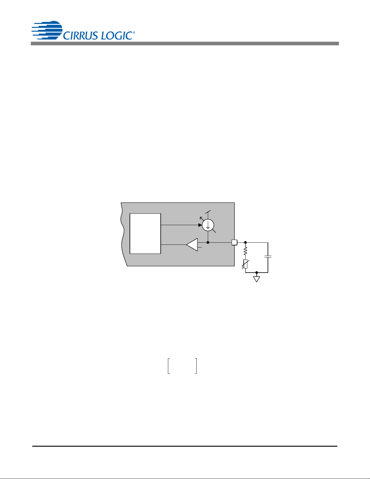
Figure 1. Block Diagram of CS1612/13 Design
3 Design Process
The design process for a two-stage power converter system can be partitioned into six circuit blocks (see Figure 1).
The AC line voltage is passed through an electromagnetic interference (EMI) filter to suppress conducted interference found on the power line. The output of the EMI filter is then converted to the desired DC output by a boost-buck
converter. The power converter system includes the Gate Bias, Steady State Supply, and Active Clamp support circuitry.
3.1 Operating Parameters
To initiate the design procedure, a set of operating parameters is required. Operating parameters required for
the analytical process are outlined in the table below. Parameters critical to the overall design, but not
specifically addressed in this document, include: EMI compliance, efficiency, footprint, layout, and operating
temperature.
Output Power
AC Line Input Voltage
Output Voltage
Parameters Symbol
Load Current
Maximum Switching Frequency*
4 AN372REV1
* Increasing FSW may reduce the size of the magnetics but increases switching losses in the FET.
P
OUT
V
V
OUT
I
OUT
F
SW(max)
IN
Page 5

3.2 Overview of Design Steps
The CS1612/13 LED driver IC controls a power converter system that has two distinct power-conversion
stages. The IC requires supporting circuitry to provide a steady-state power supply with gate bias, a clamp
circuit, and EMI filtering. The recommended design process is outlined below:
1. Start with the buck stage.
2. Design for full power at minimum V
parameters.
3. Optimize the buck stage through validation and design iteration.
4. Base the boost stage design on the power requirement of the buck stage.
5. Start the boost stage design in No-dimmer Mode.
6. Determine the peak current in the boost inductor, I
7. Determine a boost inductance, L
Consider the impact on the EMI.
8. Pick the boost FET based on peak current ratings.
9. Choose the power supply components.
10.Complete the non-power-converting circuitry: ZCD, OVP, eOTP, Clamp Circuit, Charge Pumps, and Bias
Circuits.
11. Design the EMI filter.
12.Lay out the PCB.
. Note that any design may require trade-offs for different operating
BST
PK(BST)
, that adjusts the switching frequency within the defined range.
BST
.
AN372
The buck stage design is carried out at the full brightness (full load) point. To achieve an optimal solution,
several iterations of the design process may be required. The EMI filter is particularly critical because there is
a small degree of freedom in selecting the EMI component values that meet the requirements below:
• Comply with EMI regulations
• Achieve compatibility with the largest variety of dimmers
• Smooth dimming, no flicker with a variable number of identical lamps controlled by one dimmer
AN372REV1 5
Page 6
3.3 Buck Stage Design
Buck Specification
Determine N, Fsw,
V
Refle cted
, and V
CLAMP
Estimate T3
Calculate TT
fb
Calculate R
Sense
,
R
FBG AIN
, and Buck
Inductance
R
Sense,RFBG AIN
Fit?
Yes
No
Calculate T1,
T2, and I
PK(FB)
Calculate RMS Current
and Output Capacitor
Buck Inductor
Specification
Steps for the Buck Design
1. Select a buck topology
2. Set the boost output voltage, V
BST
.
3. Select a FET that aligns with the quality standards of the
designer’s company.
4. Determine the inductor turns ratio from the
V
BST
, FET
voltage, and reflected voltage, V
Reflected
.
5. Use the nominal switching frequency and an initial
estimate for time T3 to determine the value of time TT at
full brightness.
6. Use V
BST
, TT, and V
Reflected
to determine times T1 and T2.
7. Use times T2 and TT, turns ratio N, and load current to
determine the value of the peak primary current, I
PK(FB)
.
8. Use I
PK(FB)
to determine R
Sense
.
9. Calculate the buck inductance L using time T1.
10. Calculate second stage gain resistor R
FBGAIN
using full
load conditions. Ensure linearity of the load versus the dim
curve.
11. Calculate RMS currents in the two windings of L using
peak current I
PK(FB)
and duty cycle.
12. Select an output capacitor.
13. Determine the buck inductor specifications.
14. Determine if the buck inductor fits into a specified form
factor after designing and constructing the buck inductor.
Repeat steps 3 to 12 until form factor criteria is met.
15. Refinements to the circuit with final buck inductor design.
16. Validate that the system meets the operating criteria.
Figure 2 illustrates the steps for designing the buck stage.
AN372
6 AN372REV1
Figure 2. Buck Stage Design
Page 7

AN372
Step 1) Choosing a Buck Topology
The first step in designing the buck stage is to choose a tapped buck or a normal buck. Consider the following
advantages and disadvantages of either solution:
Normal Buck Tapped Buck
Most effective with low V
High peak current; low duty cycle Low peak current; high duty cycle
Simple low-value inductor Two windings of different turns and gauges
Reduced quasi-resonant advantage Take advantage of the near zero-voltage switching
Leakage inductance L
no snubber is required
Low inductance L allows for high oscillation
frequency
Load current has lower RMS ripple and no
discontinuity; visualize Figure 1 for N=0.
Higher bulk capacitor ripple current Lower bulk capacitor ripple current
Higher bulk capacitor value Lower bulk capacitor value
Higher conduction losses Lower conduction losses
May be bound by minimum switching period T1
limitations
Lower FET voltage stress Higher FET voltage stress
Higher FET current stress Lower FET current stress
BST/VOUT
losses are not an issue, so
K
The tapped buck is best suited for a high V
ratios Most effective with high V
losses may require a
K
BST/VOUT
Leakage inductance L
snubber but may self-snub by the inductor winding
capacitance
High inductance L and high parasitic capacitance
gives low oscillation frequency
C
P
Load current has higher RMS ripple and a
discontinuity step; see Figure 1
Switching period T1 can be extended proportionally
to turns ratio N
ratio. The best approach to guarantee the most
BST/VOUT
ratios
convenient buck topology choice is to complete a preliminary design for both, and then determine whether
parameter results are impractical or out of range for the available technology and cost constraints.
AN372REV1 7
Page 8
AN372
C5
R21
Q4
GND
GD
FBSENSE
CS1612/13
BST
D3
L4
I1
V
OUT
N:1
C
P
I2
L
K
N turns 1 turn
Figure 3. Buck Converter
Figure 3 illustrates a generic implementation of a buck converter using a tapped inductor topology. A normal
buck stage can be implemented by neglecting the N turn's extension. The load is composed of a string of
LEDs. Diode D3 is the catch diode, also known as the free wheeling diode, and its function is to allow the
current to flow in inductor L4 and to the load after FET Q4 opens. Capacitance C
parasitic capacitance associated with the FET drain node, usually consisting of the FET drain-source
capacitance, inductor winding capacitance, diode D3 reverse bias capacitance, and any additional snubbing
capacitance that may be required.
V
represents the combined
P
8 AN372REV1
Leakage inductance, represented by L
labeled N turns and 1 turn are tightly coupled; the stray flux is represented by the uncoupled inductance L
Leakage inductance L
the normalized winding turns. The real inductor will have T turns and (N
is not a concern in a normal buck (non-tapped) design. Inductor winding N and 1 are
K
, is inevitably associated with a tapped inductor. Inductor windings
K
T) turns.
.
K
Page 9
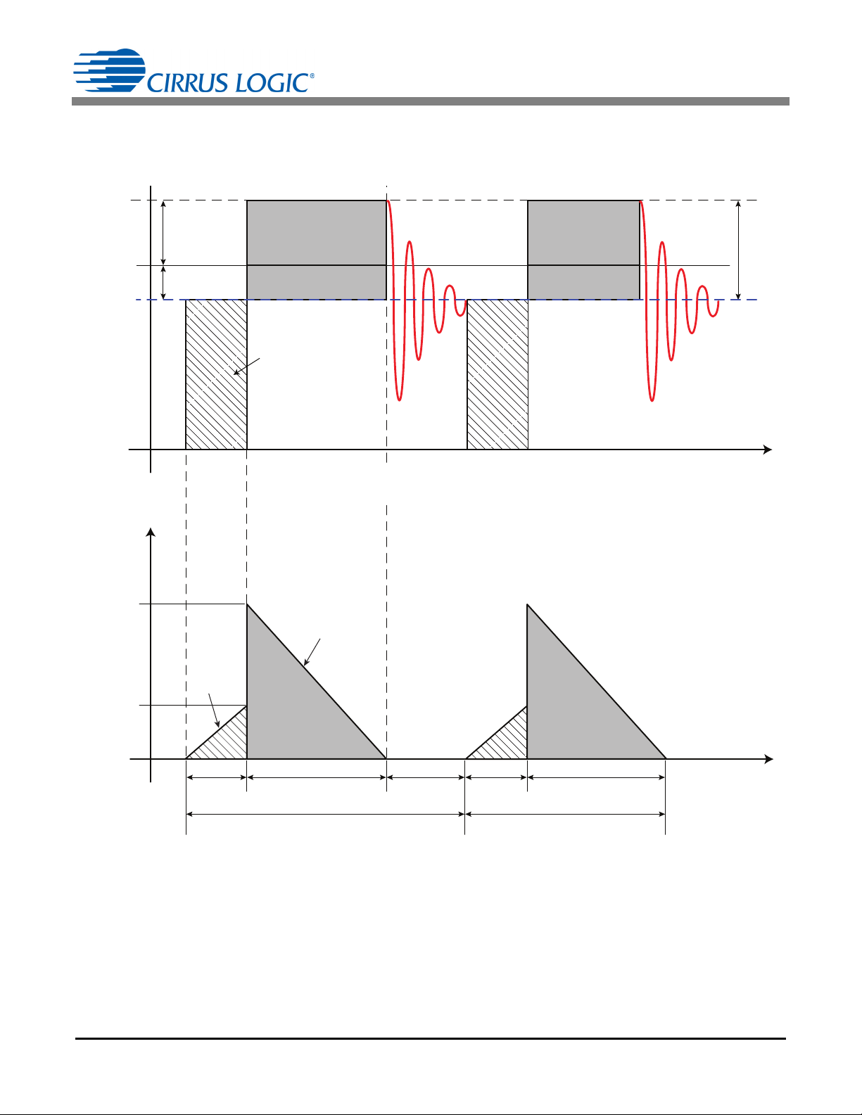
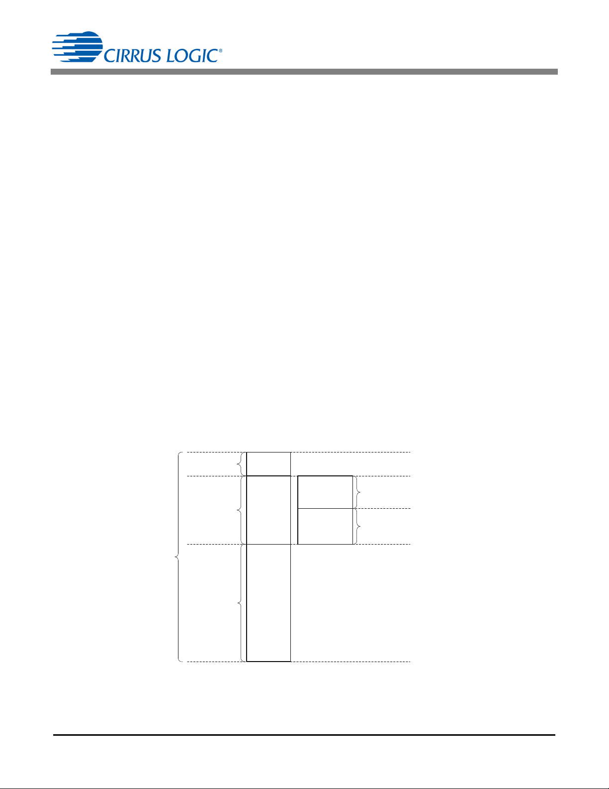
AN372
Area = N ު V
OUT
ު T2
Area = V
OUT
ު T2
Area = (V
BST
- V
OUT)
ު T1
V
BST
V
ZERO
N ު V
OUT
V
OUT
t
V
Reflected
Figure 4a. FET Drain Voltage
T1
TT
T3
'
C
1- '
C
T2
1
I
PK(FB)
t
(N+1)
ު I
PK(FB)
I1
I2
Figure 4b. Current Through FET Q4 and Diode D3
The buck stage is supplied by the boost output voltage. The boost output voltage is regulated within 10% by
the boost stage. The buck control loop regulates the output current as long as the peak current has sufficient
margin to rise 10% at the lowest boost output voltage. Figure 4a and Figure 4b show idealized waveforms of
the FET Q4 drain voltage and drain current and the diode D3 current.
AN372REV1 9
Page 10
AN372
V
Drain maxVBST maxVCLAMP max
+=
[Eq. 1]
V
OvershootVCLAMPVReflecteed
–=
[Eq. 2]
V
Margin
V
CLAMP
V
BST
V
Overshoot
V
Reflected
ET Breakdown
Voltage Rating
Clamp
Voltage
Boost Output
Voltage
Margin
Reflected
Voltage
Overshoot
Voltage
Overshoot is a brief condition
above V
Reflected
, required to
quickly dissipate the energy
stored in the inductor leakage,
L
K
.
During this time, the primary
current is kept from
transferring to the secondary,
siphoning energy from the load
to the clamp zener (snubber).
Figure 5. FET Breakdown Voltage
Step 2) Select a Value for Boost Output Voltage
The value of the boost output voltage, V
The maximum V
voltage, V
BST
BST(max)
requirement within economical constraints.
V
is determined by an internal parameter and changes slightly depending on the type of dimmer detected.
BST
With sense resistors R7, R8, R14, and R15 set to 1.5M, the resulting V
system. For a 120V system, sense resistors R7, R8, R14, and R15 are set to 750k each, and the resulting
V
is approximately 200V. V
BST
each half line-cycle. V
droops to its lowest value towards the end of each half line-cycle until the boosting
BST
is regulated by charging the boost output capacitor to its nominal value
BST
process starts again in the next half line-cycle.
Step 3) Select an Appropriate FET
Determine the FET breakdown voltage, V
voltage, V
Drain(max)
, is calculated using Equation 1.
, must be greater than the maximum input AC line voltage peak.
BST
, should be kept as low as possible to help maintain the FET breakdown
is approximately 405V for a 230V
BST
Breakdown
, and reflected voltage, V
Reflected
. The FET maximum drain
The ringing associated with the inductor leakage, L
, usually does not have enough energy to cause a
K
destructive avalanche breakdown. Voltages closely approaching the FET breakdown voltage are acceptable.
Ideally, V
Reflected
near 50% duty cycle optimizes efficiency. Alternatively, V
rapidly discharge the energy stored in the inductor leakage, L
should have nearly the same value as V
because operating the tapped buck inductor at
BST
should be much greater than V
CLAMP
K
.
Reflected
to
The FET breakdown voltage is constrained by cost and performance. A compromise must be reached in
partitioning voltage between V
divide V
CLAMP
into V
Reflected
The losses caused by the leakage inductance are inversely proportional to V
BST
, V
CLAMP
, and V
. A second compromise will then determine how to
Margin
and a reasonable overshoot voltage portion, V
Overshoot
Overshoot
.
, which is determined by
Equation 2.
F
10 AN372REV1
Page 11

AN372
V
Breakdown
V
BSTVReflected
V+
CLAMP
V
Reflected
– V
Minarg
++=
[Eq. 3]
N
V
Reflected
V
OUT max
----------------------------=
[Eq. 4]
T1 T2+
1
F
SW
-----------
T3–=
[Eq. 5]
For optimum efficiency, the increase in conduction losses (created by an uneven duty cycle) must balance the
reduction of the losses caused by discharging the leakage inductance (obtained by increasing the overshoot
voltage). Equation 3 is used to balance all voltages contributing to the FET voltage drain and source.
where
V
Overshoot
Step 4) Determine the Buck Inductor Turns Ratio
Select a turns ratio based on the output voltage, V
where
V
OUT(max)
Step 5) Select the Full Brightness Switching Frequency
The CS1612/13 maximum switching frequency is 200kHz. Test results indicate that optimal performance is
obtained in the range of 75kHz to 120kHz. Higher frequencies allow the use of smaller magnetics, but
switching losses increase. Selecting too low a full brightness switching frequency risks impairing dimmer
compatibility while also allowing the minimum frequency to drop into the audible range.
From the full brightness frequency, determine the value of (T1+T2) using Equation 5.
= V
CLAMP
- V
Reflected
OUT
, and V
= The maximum LED string forward voltage V
Reflected
at full current plus the rectifying diode voltage V
OUT
using Equation 4.
F
where
T3 is 1/2 the resonant period
The boost inductance resonates with the total parasitic capacitance of the drain node. For initial calculations,
T3 is estimated as 1s and must be measured for final accuracy.
During full brightness circuit operation, the circuit is delivering full nominal power to the LED string. When Q4
turns ‘ON’, current flows through the LED string, the entire inductor L winding (N+1), FET Q4, and resistor
R
(R21).
Sense
The current rises linearly from zero to a preset maximum value I
threshold. The gate is driven high for as long as is required to reach I
PK(FB)
PK(FB)
defined by R
and the internal IC
Sense
. The controller has a maximum T1
(‘ON’ time) limit set to 8.8s, after which the gate is turned ‘OFF’.
Just before the gate turns ‘OFF’ the inductor has a field strength of ((N+1)I
). When the gate turns
PK(FB)
‘OFF’, the field cannot change abruptly, despite the fact that current no longer flows though N turns. Therefore,
a current equal to ((N + 1) I
) must flow in the single turn left in the circuit. A tapped inductor enables
PK(FB)
current multiplication in the load path in exchange for a longer rise time T1 and higher reflected voltage across
the FET (see Figure 6).
During time T2, the inductor current decays linearly, transferring to the load the energy stored in the inductor.
At the end of time T2, the current in the inductor is zero. However, some energy is stored in parasitic
capacitance C
the energy stored in C
energy is still stored in the capacitor and with the right voltage polarity to facilitate the charge to (V
charged to ((N+1)V
P
. By turning ‘ON’ the FET Q4 at the end of the first half of the oscillation, most of the
P
). Capacitance CP and inductance L oscillate until the losses exhaust
OUT
BST-VOUT
required by a new cycle start.
This mode of operation with minimal time between the end of time T2 and the new cycle start is called quasiresonant and is maintained only at full power or near full power. At lower power levels, one or more extra
oscillations are allowed before turning ‘ON’ the FET Q4 at the next valley. Extending the idle time T3, when no
)
AN372REV1 11
Page 12

AN372
T1
T2 T3
V
DS
t
Figure 6. Timing Diagram of Times T1, T2, T3, and TT
V
BSTVOUT
–T1N1+V
OUT
T2– 0=
[Eq. 6]
T2
T1
------ -
V
BSTVOUT
–
N1+V
OUT
--------------------------------------- -
=
[Eq. 7]
current flows in the load circuit, dilutes the energy delivered during time T1 and T2 resulting in lower average
power to the load.
Dimming Operation
The dimmer conduction time or phase cut information is extracted by the boost stage and supplied to the buck
stage as a digital parameter, dim, ranging from 0.02 to 1 as a measure of the normalized output power to be
delivered. The dim parameter controls both the normalized peak current in the inductor and the total period
TT. Reaching a lower peak current requires less time T1 and consequently less time T2 to discharge the
inductor; at the same time, the idle time T3 is increased to keep the total period TT nearly constant. Doing so
reduces power, maintaining constant frequency, until the peak current is halved. Further power reduction is
obtained increasing the period TT without reducing the current.
When the current is moderately reduced, time T3 is increased just enough before turning ‘ON’ FET Q4 during
the second or third valley sustaining the quasi-resonant mode of operation. At deeper dimming levels, reducing
the switching frequency also reduces the capacity losses; therefore, enforcing a quasi-resonant mode is no
longer a requirement, and the oscillatory transient is left to decay until a new cycle is started at the calculated
TT.
Basic Design Equation
The DC voltage across any winding must be zero. The entire winding (N+1) is subject to voltage (V
during time T1 and subject to voltage ((N+1) x V
) during time T2. The average voltage across L is
OUT
BST
- V
OUT
)
calculated using Equation 6:
Solving Equation 6 for ratio T2/ T1:
12 AN372REV1
Page 13

AN372
TT T1 T2+=
[Eq. 8]
C
T1
TT
-------
=
V
OUT
N1+
NV
OUT
V
BST
+
--------------------------------------------------
=
[Eq. 9]
C
V
OUT
V
BST
--------------
=
[Eq. 10]
T1
1
F
SW
----------- T 3–
V
Reflected
V
ReflectedVBST
+
----------------------------------------------------
=
[Eq. 11]
T2
1
F
SW
----------- T 3–
V
BST
V
ReflectedVBST
+
----------------------------------------------------
=
[Eq. 12]
I
PK FB
2P
OUT max
TT
fb
V
BST
T1fb
----------------------------------------------
=
[Eq. 13]
R
Sense
1.4
I
PK FB
------------------=
[Eq. 14]
Initially, T3 is assumed to be zero. After the circuit is built, the oscillation period can be measured, and the
circuit parameters can be tuned to assure full power at the nominal switching frequency. Setting T3 to zero
defines the total switching period TT as:
solving for the critical duty cycle
using Equation 7 and Equation 8 yields:
C
where
= Critical duty cycle
C
For a normal buck topology N = 0 and Equation 9 reduces to:
Typically 180V < V
< 450V and V
BST
on the denominator. Therefore, an estimate of
T1 and decreases period T2, which decreases the peak current I
< 30V. The effect N has on the numerator of
OUT
is roughly proportional to N. Increasing N increases period
C
PK(FB)
current in the second stage catch diode D3.
Step 6) Determine the Buck Nominal Timing T1 and T2
Equation 11 and Equation 12 express T1 and T2 from TT and
∆
, accounting for the effect of non-zero T3.
C
Solve for T1 and T2 using Equation 11 and Equation 12, respectively:
is greater than it is
C
in the FET but increases the peak
Step 7) Calculate Peak Current on the Buck Primary-side
Calculate I
using Equation 13:
PK(FB)
where
TT
= Switching period at full brightness (full load condition)
fb
T1
= Period T1 at full brightness (full load condition)
fb
Use values that yield the highest I
Step 8) Calculate R
Calculate sense resistor R
Sense
Sense
PK(FB).
(R21)
(R21) for buck using Equation 14:
where
R21 = R
Sense
in
AN372REV1 13
Page 14

Step 9) Calculate the Buck Inductance (as Measured Across the N+1 Turns)
L
V
BSTVOUT
–T1
I
PK FB
---------------------------------------------------- -
=
[Eq. 15]
R
FBGAIN
62.5k
TT
fb
T2
fb
----------- -
2
1–
------------------------------------
=
[Eq. 16]
I
RMSIPK FB
T
current
3TT
--------------------
=
[Eq. 17]
I
PK FB
V
BSTVOUT
–T1
L
---------------------------------------------------- -
=
[Eq. 18]
T2
N1+L
N
2
VO
----------------------------
=
[Eq. 19]
AN372
Step 10) Calculate R
FBGAIN
Use Equation 16 to calculate the second-stage gain resistor R
(R17)
FBGAIN
(R17).
where
R17 = R
TT
= Switching period TT at full brightness (full load condition)
fb
T2
= Period T2 at full brightness (full load condition)
fb
FBGAIN
in
Step 11) Determine the RMS Current in the Winding
Determining the RMS current, I
, is necessary to properly define the wire size. Use Equation 17 to calculate I
RMS
RMS
where
T
= Time when the current is present in the winding
current
TT = T1+T2 + T3 (see Figure 4b)
The factor 3 accounts for the current triangular shape
Step 12) Determine Output Capacitor
The buck output capacitor must provide a low impedance to the switching frequency. When using an
electrolytic capacitor, the choice is based on its ability to carry the ripple current to provide a long service life.
Meeting the ripple, voltage, temperature and lifetime requirements yields a high value capacitor, often greater
than what is required for current handling. In buck applications, the voltage ripple across the output electrolytic
capacitor is determined mostly by the ESR rather than the reactance.
Step 13) Buck Inductor Specification
This step is the first iteration of the inductor design. Due to design constraints, the following requirements must
be met:
• The core must be big enough to fit the windings.
• The number of turns required must fit in the bobbin, along with insulation material.
• The finished inductor must not overheat in the environment.
• Magnetic and geometric constraints may not yield the exact value of L and N calculated.
Once the first iteration of the design is done, calculate the new I
to maintain the same T1 time as earlier
PK(FB)
using the actual value of L, as shown in Equation 18.
:
Calculate the new T2 value using the new I
and N, as shown in Equation 19:
PK(FB)
14 AN372REV1
Page 15

AN372
FB
Gain
TT
fb
T2
fb
------------
V
BST
NV
OUT
+
V
BSTVOUT
–
--------------------------------------------------==
[Eq. 20]
1FB
Gain
2.5
[Eq. 21]
T2fbTTfb2.5 T 2
fb
0V
Reflected
1.5 V
BST
15.6k R
FBGAIN
62.5k
[Eq. 22]
First Valley
Buck FET
Voltage
V
CLAM P
V
BST
V
Reflec ted
Figure 7. Switching Waveform of Buck FET Drain
Step 14) Circuit Adjustments
Circuit adjustments are required after the inductor has been designed and constructed. Recalculate resistor
R
FBGAIN
The second-stage gain, FB
FB
which has the following implications:
using Equation 16.
, is an internal constant that is programmable by resistor R
Gain
is used in the second-stage algorithm to control the switching period, TT. The range of FB
Gain
FBGAIN.
Gain
is limited to
:
If FB
situation, a high I
the FET breakdown voltage. If the value of FB
range of V
lower I
The duration of time T1 is determined by the time it takes the primary current to reach I
is close to 1, the duty cycle will be low, which will cause a low reflected voltage, V
Gain
PK(FB)
to (1.5V
BST
, requiring a higher FET breakdown voltage.
current is required to reach full brightness, and the only advantage would be to lower
PK(FB)
), resulting in a duty cycle that is between 50% and 60%. This setting causes a
BST
were in the range of 2 to 2.5, then V
Gain
Reflected
Reflected
PK(FB)
would be in the
, and the duration
. In this
of time T2 is dependent on the time it takes the secondary current to reach 0. To achieve the best full-power
efficiency, adjust the switching period, TT, which will start a new switching cycle after the buck FET drain
voltage has reached the valley (see Figure 7). Once the buck inductor is built, R
change TT to allow it to cycle at the valley. Adjusting R
changes the switching frequency slightly.
FBGAIN
can be adjusted to
FBGAIN
Although R
FBGAIN
could be used to control the load current, its primary purpose is to control the valley
switching range. It is recommended to adjust the load current by changing the primary current sense resistor,
R
, connected to the FBSENSE pin of the IC, and then use R
Sense
Step 15) Recalculate R
The buck primary current is controlled by comparing the voltage across R
threshold of 1.4V. To guarantee the rated LED current under worst-case conditions, when the LED string has
maximum voltage, the V
obtain the nominal LED current, then adjust R
AN372REV1 15
Sense
is at its minimum point, and R
BST
FBGAIN
is at its highest tolerance. Adjust R
Sense
to hit the valley.
to control valley switching.
FBGAIN
at pin FBSENSE to an internal
Sense
Sense
to
Page 16
AN372
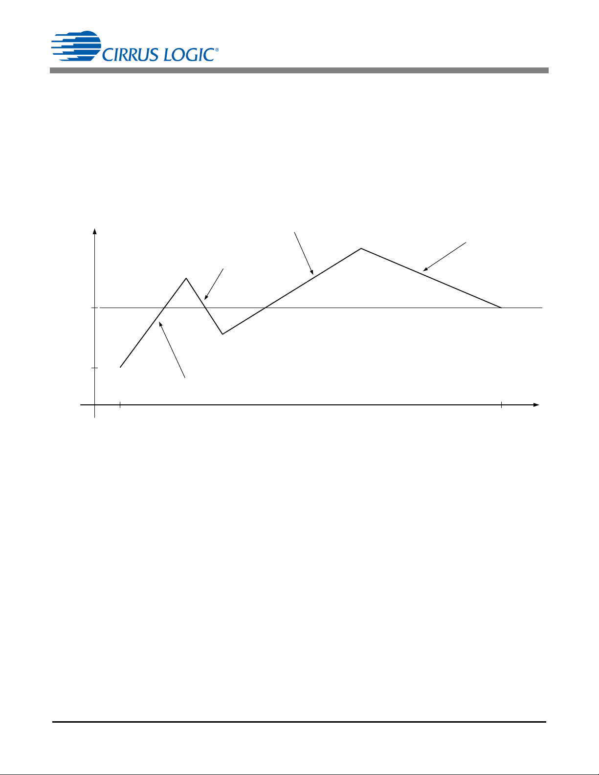
5% Light
100% Light
(F ull Brigh t)
F
sw(fb)
>F
MIN
Switching Frequency, F
sw
Further peak current reduction
and frequency increase
still reducing aver age curr ent
Increasing T2 at reduced peak current
CRM with valley switching region. Reducing peak
current for ces a frequency increase.
Increasing T2 at minimum peak current
Dimming
Figure 8. Buck Switching Frequency Profile vs. Dimming
Notes on Circuit Fine Tuning
• Going beyond the R
• R
Sense
and R
FBGAIN
FBGAIN
• The optimized final design will have a slightly different switching frequency variation than the first design
iteration.
• When the load is increased or decreased by 10%, then R
than 10%, respectively. Adjusting R
‘ON’ hits the resonant voltage valley.
• Figure 8 illustrates a typical frequency profile with dimming. This is only one typical profile. The breakpoints
can move depending on various tolerances and specific design choices.
limitation will not have any further effect on the design.
are frequently adjusted simultaneously to reach the desired operating point.
needs to be decreased or increased by less
is required when the load changes so that the buck FET turn
FBGAIN
Sense
At this point, full power and valley switching are close to the target frequency. Further adjustment of the
frequency is done by changing the buck inductor primary inductance, L. The core gap can be changed for small
inductance variations.
16 AN372REV1
Page 17

3.4 Boost Stage Design
I
PK BST
3.64 PIN
V
RMS
-------------------------- -
=
[Eq. 23]
The design process for the boost stage is outlined below:
1. Determine I
PK(BST)
and a tentative resistor value, R
2. Determine boost inductor specifications
3. Calculate boost input and output capacitors
The boost stage is designed in No-dimmer Mode, which has a considerable degree of freedom in its design
parameters. For the boost stage to operate in dimmer mode and with the largest variety of dimmers, the design
is constrained within a more limited set of parameters. Even in No-dimmer Mode, the several operating states
of the boost stage make an exclusively formula-based design impractical.
IPK
(R13)
AN372
Step 16) Determine I
PK(BST)
, I
SAT
, and R
IPK
(R13)
The boost stage peak current has two distinct values:
• I
PK(BST)
is related to the input power, PIN. The boost inductor current reaches this value during a substantial
portion of the line-cycle, affecting the RMS value of the inductor and line current.
• I
is a constant value of 0.6 A and is independent of the power level. I
SAT
dimmer TRIAC in the conduction mode. I
is a brief duration that immediately follows the dimmer firing
SAT
is necessary to maintain the
SAT
and has a minimal impact on RMS current and its heating effects. The boost inductor must be capable of
carrying the current I
without saturating.
SAT
The factor 3.64 accounts for a factor of 2 due to the triangular waveform, a factor of 1.41 due to the voltage
sinusoidal shape, and a factor of 1.29 derived by simulation accounting for the line current envelope profile.
The current envelope profile approximates a sine wave in a stepped fashion according to the following
conditional rules:
• IF V
• IF V
• IF 45° <Phase <135° AND V
• IF 45° < Phase < 135° AND V
• IF V
Boost output voltage V
< 60V THEN I
LINE
> 60V AND Phase > 20° THEN the boost inductor peak current equals 0.75 I
LINE
< 60V OR Phase > 160° THEN I
LINE
PK(BST)
is regulated by controlling the time when the current is held equal to I
BST
equals 0
< V
BST
> V
BST
THEN the inductor current peak equals I
MAX
THEN the inductor current peak equals 0.75 I
MAX
PK(BST)
equals 0
PK(BST)
PK(BST)
PK(BST)
PK(BST)
during
the central portion of the period between 45° and 135°.
Figure 9 shows the inductor peak current envelope and the AC line current waveform at nominal voltage in Nodimmer Mode.
AN372REV1 17
Page 18

AN372
0.00
0.02
0.04
0.06
0.08
0.10
0.12
0.14
0 15 30 45 60 75 90 105 120 135 150 165 180
Current (A)
Phase Angle (°)
AC Line Current
Inductor Peak Current
Figure 9. Current vs Phase Angle
[Eq. 24]
R
IPK
15.625 103V
I
PK BST
------------------------------------------ -
=
The AC line current does not follow the inductor peak current envelope because the circuit operates in CRM
and DCM. The switching frequency and duty cycle changes across the AC line phase resulting in a changing
average value after the EMI filter smoothing.
Once I
PK(BST)
is determined, R
drive current sink, which is equal to I
During circuit adjustment, connect an electronic load in CV mode for testing and clamp protection. Set the
must be calculated. I
IPK
PK(BST)
. See Equation 24:
PK(BST)
sets the maximum value for the internal source
electronic load so that the boost output voltage is 425V for a 230V system or 215V for a 120V system.
Measure switching frequency at a fixed V
voltage, as shown in Figure 9.
voltage. Adjust I
rect
PK(BST)
to obtain the desired waveform at the mid
Step 17) Boost Inductor Specifications
The CS1612/13 controls I
PK(BST)
only controls the average switching frequency. The instantaneous frequency changes to meet the I
imposed by the controller and the duty cycle imposed by the CRM/ DCM algorithm.
and keeps the boost stage operating in CRM. The boost inductance L
The boost inductor should be designed for 600mA at 3000 Gauss. For a given input voltage design, the product
of (L
product, and divide the product by P
BST
P
) is constant. Choose the frequency range on Figure 10 to find the corresponding (L
IN
to obtain L
IN
BST
.
18 AN372REV1
PK(BST)
PIN)
BST
BST
Page 19
AN372
0
10
20
30
40
50
60
70
80
90
100
110
120
130
140
10 20 30 40 50 60 70 80 90 100 110 120 130 140
120V Min Freq
120V Max Freq
230V Min Freq
230V Max Freq
Power Multiplied by Inductance (Watts Multiplied by mH)
Switching Frequency (kHz)
Figure 10. Switching Frequency vs Power Inductance
The frequency range should be as high as possible without exceeding 75kHz. This strategy will keep the
fundamental and second harmonic below the 150kHz EMI requirements.
In most low-power designs, the boost inductor peak current I
PK(BST)
Specify the boost inductor turns such that the core will reach 3000Gauss when the current equals 600 mA. To
protect against runaway, set the artificial load to a constant voltage to achieve nominal
value of R
to obtain the nominal boost output current, I
IPK
BST(nominal)
Measure the switching frequency in the high current region in the 45° to 90° AC phase angle range. Adjust the
boost inductor value to determine the desired frequency. Adjustments to the inductor value are made by
changing the gap. Increasing the gap is always safe, but reducing the gap may saturate the core. It may be
beneficial to redesign the boost inductor if changes to the inductor gap are greater than 20%.
Step 18) Determine Boost Output Capacitor
is much higher than the RMS value.
.
V
, then adjust the
BST
The boost stage output capacitor is also the buck stage input capacitor. Determine the size of the boost output
capacitor using the following points:
• For a 120V line input system, capacitor C4 > 2F/Watt of input power
• For a 230V line input system, capacitor C4 > 0.5F/Watt of input power
Proper capacitor size is required to ensure that the following dimmer algorithms execute properly:
• Transition CCM to CRM properly
• No erroneous CCM events
• No CCM operation with trailing-edge dimmers
• No CCM operation in No-dimmer Mode
• Boost and buck stages loop stability
AN372REV1 19
Page 20

Step 19) Determine Boost Input Capacitor
V
DDVZ1VQ2 thVD6
––=
[Eq. 25]
V
DD
VZ1V
Q1 th
–VZ1V
Q2 thVD6
––=
[Eq. 26]
N
P
N
AUX
--------------
V
BST
22
--------------=
[Eq. 27]
To be compatible with a wide range of dimmers, the boost input capacitance should be minimized. Large input
capacitance impacts the ability of the controller to properly sustain the current required by the dimmer and may
cause oscillation. Capacitors should not be connected to the AC line side of the bridge rectifier. Added AC lineside capacitance alters the dimmer behavior in multi-lamp configurations and shifts the dimming curve.
Excessive capacitance (C1) after the bridge generates current spikes that may introduce ringing. The ringing
will cause a TRIAC to prematurely open its switches.
3.5 Completing the Design
Step 20) Choose Power Components
The voltage rating of boost FET Q2 and diode D1 can be estimated by adding 20% to the V
standard margin for safety purposes and prevents damage to the components during abnormal or transient
conditions. Lower voltage ratings can be used, but sufficient testing is necessary to ensure proper operation.
V
is 405V or 200V for an AC input voltage of 230 VAC or 120VAC, respectively. The breakdown voltage
BST
for both the FET Q2 and the boost diode D1 ≥
(1.2 V
). The boost diode must be ultrafast with a recovery
BST
time no greater than 50ns and rated for a DC current, as calculated using Equation 23.
Step 21) Bias Circuit
The bias circuit is built using components C2, C8, C12, R4, D4, D7, and Z1 (see Figure 1 on page 4). When
AC power is first applied, current flows through capacitor C2 charging capacitor C8, which biases boost FET
Q2 into conduction. Once the bias circuit turns ‘ON’ boost FET Q2, a current is applied to pin VDD through
diode D6.
The initial supply current I
charge on capacitor C8.The initial supply voltage V
flows through FET Q2 onto capacitors C10 and C6. Zener diode Z1 limits the
DD
applied to pin VDD is defined by Equation 25:.
DD
. 20% is a
BST
AN372
Resistor R4 limits the current in capacitor C2. Once the voltage applied to pin VDD has exceeded the UVLO
voltage, the CS1612/13 starts to operate, and voltage appears at the boost inductor L3 auxiliary winding.
When FET Q2 is ‘ON’, capacitor C9 charges from diode D5 to pin GND. When FET Q2 is ‘OFF’, capacitor C9
reroutes the charge into capacitor C6 from diode D5. As the voltage develops across capacitor C6 and
exceeds V
, FET Q1 turns ‘ON’, and diode D6 reverse biases. After startup, FET Q1 supplies VDD to the
DD
device with the larger current required during normal operation. See Equation 26:
The inequality in Equation 26 indicates that D6 is back biased after start up.
Step 22) Zero-current Detection
The CS1612/13 uses zero-current detection (ZCD) to minimize switching losses. The ZCD algorithm is
designed to turn ‘ON’ the FET when the resonant voltage across the FET is at a low point (see Figure 7). Valley
switching reduces the CV
2
power losses associated with rerouting charge from the body capacitance of the
FET. Similar approaches are taken when turning ‘ON’ the boost FET Q2 and the buck FET Q4. Pin BSTAUX
and FBAUX are designed to monitor the resonant voltage from the auxiliary winding of the boost inductor L3
and the buck inductor L4, respectively. The buck ZCD and the boost ZCD function in exactly the same manner.
As described in step 21, the auxiliary winding of the boost inductor L3 is also used to drive the charge pump
circuit to develop the supply voltage, V
. It is recommended to use the boost auxiliary winding for the boost
DD
ZCD. The buck inductor L4 auxiliary winding monitors output overvoltage and the ZCD function. The auxiliary
winding turns ratio must be designed to develop ~22V peak-to-peak under nominal conditions. The turns ratio
for L4 is calculated using Equation 27:
20 AN372REV1
Page 21
AN372
CS1612/13
+
-
I
CONNECT
V
CONNECT
(th )
Comp_Out
eOTP
Control
eOTP
R
S
C
NTC
NTC
V
DD
10
(Optional )
Figure 11. eOTP Functional Diagram
I
CONNECT
V
CONNECT th
R
-------------------------------------=
[Eq. 28]
CODE
I
CONNECT
2
N
-------------------------- -
V
CONNECT th
R
NTCRS
+
-------------------------------------=
[Eq. 29]
The BSTAUX pin and FBAUX pin currents must be limited to less than 1mA. A series resistor of at least 22 k
must be used to limit the current.
Step 23) Overvoltage Protection
Output open circuit protection and output overvoltage protection (OVP) are implemented by monitoring the
output voltage through the buck inductor auxiliary winding. During switching time T2, the voltage across the
buck inductor L4 auxiliary winding is representative of the output voltage using a turns ratio relationship. The
buck auxiliary winding voltage is applied to the FBAUX pin. If the voltage on the FBAUX pin exceeds a
threshold V
restart after one second.
Since the buck auxiliary winding does not supply V
constraints. A buck auxiliary output voltage of 10V to 20V during switching period T2 is appropriate. The
resistive divider between the buck auxiliary winding and the FBAUX pin must be sized to produce 1.25V when
an overvoltage fault occurs at the desired load. The FBAUX pin current must be limited to less than 1mA.
Step 24) External Overtemperature Protection
The eOTP pin is used to implement overtemperature protection using a negative temperature coefficient
(NTC) thermistor. The total resistance on the eOTP pin is converted to an 8-bit digital ‘CODE’ (which gives an
indication of the temperature) using a digital feedback loop, adjusting current I
series resistor R
functional block diagram when connecting an optional NTC temperature sensor to the eOTP circuit.
of 1.25V, a fault condition occurs. The IC output is disabled and the controller attempts to
OVP(th)
, the auxiliary winding circuit has fewer design
DD
into the NTC and
to maintain a constant reference voltage V
S
CONNECT(th)
CONNECT
of 1.25V. Figure 11 illustrates the
Current I
CONNECT
is generated from an 8-bit controlled current source with a full-scale current of 80A. See
Equation 28:
When the loop is in equilibrium, the voltage on the eOTP pin fluctuates around V
‘CODE’ output by the ADC is used to generate I
CONNECT
. In normal operating mode, the I
CONNECT(th)
. The digital
CONNECT
updated once every seventh half line-cycle by a single ±LSB step. See Equation 29:
AN372REV1 21
current is
Page 22

Solving Equation 29 for CODE:
CODE
2
N
V
CONNECT th
I
CONNECT
R
NTCRS
+
-------------------------------------------------------------------
=
256 1.25 V
80AR
NTCRS
+
-----------------------------------------------------------
=
4M
R
NTCRS
+
---------------------------------
=
[Eq. 30]
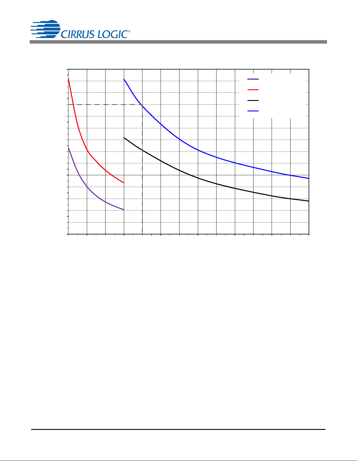
Temperature (°C)
Current (I
LED
, Nom.)
125
95
50%
100%
0
25
Figure 12. LED Current vs. Temperature
AN372
The tracking range of this resistance ADC is approximately 15.5k to 4M. The series resistor R
is used to
S
adjust the resistance of the NTC to fall within this ADC tracking range so that the entire 8-bit dynamic range of
the ADC is used. A 14 k (±1% tolerance) series resistor is required to allow measurements of up to 130°C to
be within the eOTP tracking range when a 100k NTC with a Beta of 4334 is used. The eOTP tracking circuit
is designed to function accurately with an external capacitance of up to 470pF. A higher 8-bit code output
reflects a lower resistance and hence a higher external temperature.
The ADC output code is filtered to suppress noise and compared against a reference code that corresponds
to 125/130°C. If the temperature exceeds this threshold, the chip enters an overtemperature state and shuts
down. This is not a latched protection state, and the ADC keeps tracking the temperature in this state in order
to clear the fault state once the temperature drops below 110 °C. If an external overtemperature protection
thermistor is not used, connect the eOTP pin to GND using a 50k to 500 k resistor to disable the eOTP
feature.
When exiting reset, the chip enters startup and the ADC quickly (<5ms) tracks the external temperature to
check if it is below the 110°C reference code before the boost and second stages are powered up. If this check
fails, the chip will wait until this condition becomes true before initializing the rest of the system.
For external overtemperature protection, a second low-pass filter with a time constant of 2 seconds filters the
ADC output and uses it to scale down the internal dim level of the system (and hence the LED current, I
LED
if the temperature exceeds 95 °C (see Figure 12).
)
The large time constant for this filter ensures that the dim scaling does not happen spontaneously and is not
noticeable (suppress spurious glitches). The I
starts reducing when R
LED
~ 6.3k (assuming a 14k1%
NTC
tolerance, series resistor), which corresponds to a temperature of 95°C for a 100k NTC (100 k at 25 °C).
The I
value to scale the output LED current, I
current is scaled until the NTC value reaches 2.5k (125°C). The CS1612 /13 uses this calculated
LED
, as shown in Figure 12. Beyond this temperature, the IC shuts
LED
down. If the external overtemperature protection feature is not required, connect the eOTP pin to GND using
a 50k-to-500k resistor to disable the eOTP feature.
22 AN372REV1
Page 23

AN372
Step 25) Clamp Circuit
To keep dimmers conducting and prevent misfiring, a minimum power needs to be delivered from the dimmer
to the load. This power is nominally around 2W for 230 V and 120V TRIAC dimmers. At low dim angles (≤90°),
this excess power cannot be converted into light by the output stage because of dim mapping at light loads.
V
can rise above the safe operating voltage of the primary-side bulk capacitor C4. The clamp circuit drains
BST
excess charge from capacitor C4 by turning ‘ON’ FET Q3, dissipating the power into load resistors R6 and
R16. The clamp load resistors R6 and R16 must each be 2k 2W resistors for 230V and 500 2W resistors
for 120V systems.
Step 26) Designing the EMI Filter
The switching frequency of the CS1612/13 can cause resonance in the EMI filter, so it is important to carefully
design it. Resonance can cause undue noise, oscillation, and impact power factor. The resonant frequencies
on the LC filters must be less than 1/10 of the minimum switching frequency of the boost stage. There is a
variety of dimmers, and each behaves differently. All dimmers are sensitive to the presence of heavy EMI filters
with large capacitance or inductance. Capacitor C1 should not exceed 10nF. Capacitance on the AC side of
the rectifier should be avoided. Capacitance to the immediate output of the rectifier bridge should be minimized
for optimal dimmer compatibility.
The EMI filter and the reactances associated with the dimmer constitute a complex reactive network that has
minimal damping. This reactive network will ring as it is excited by the dimmer turn on and the boost stage
conduction. Should the current in the dimmer's TRIAC reverse, the TRIAC will open, disturbing the dimmer
timing, which results in flicker. Therefore, stringent limitations are imposed on the values assigned to the EMI
components.
Step 27) Layout
Basics for any power layout:
• Keep power traces as short as possible.
• Keep the controller away from power components and traces if possible. Keep sensitive traces (all sense
inputs) away from high dv/dt traces such as FET drain, FET gate drive, and auxiliary windings.
• Isolate control GND from power GND.
- All control components must be grounded to SGND.
- A single thick trace must connect SGND to GND and then extended to the buck current sense resistor
R21 with a short run.
- The connection between the boost output capacitor C4 and resistor R21 must be short.
• Decouple the capacitor directly at the VDD pin of the CS1612/13 to SGND.
• Run sense traces, especially current sense, away from power-carrying traces characterized by high dv/dt
(fast rise/fall times) traces such as collectors and drains of FETs Q2, Q3, and Q4 or the auxiliary windings
or the SOURCE pin.
• Further details are available in application note AN346 CS150x and CS160x PCB Layout Guidelines.
AN372REV1 23
Page 24

4 Design Example
Cmin/max
V
OUT min
V
BST max
---------------------------
=
24V 1.2V–
405V 40.5V+
-----------------------------------------
5.1%==
[Eq. 31]
Cmax/min
V
OUT max
V
BST min
--------------------------- -
=
24V 1.2V+
405V 40.5V–
---------------------------------------- -
6.9%==
[Eq. 32]
P
IN
P
OUT
---------------- -
=
9.6W
0.92
------------- -
10.5W==
[Eq. 33]
I
PK FB
2IAV
C
----------------- -
229mA
0.069
------------------------- -
== 840mA=
[Eq. 34]
P
IN
V
BST min
------------------------- -
10.5W
405V 40.5V–
---------------------------------------- -
= 29mA=
[Eq. 35]
T1
Cmin/max
TT 0.051 8s 408n s===
[Eq. 36]
T2 TT T1– 8s 408ns– 7.592s===
[Eq. 37]
The required operating parameters for the analytical process are outlined in the table below.
Parameters Symbol Value
Output Power
AC Line Input Voltage
Output Voltage
Load Current
Maximum Switching Frequency*
* Increasing FSW reduces the size of the magnetics but increases switching losses in the FET.
P
OUT
V
V
OUT
I
OUT
F
sw(max)
IN
4.1 Buck Design Steps
A switching frequency of 125kHz is selected, which corresponds to a switching period TT of 8µs.
Step 1) Choosing a Buck Topology
Normal Buck Circuit Design
A normal buck approach is used to calculate the critical duty cycle
V
OUT(min)
and maximum boost voltage V
BST(max)
. Solve for
C(min/max)
C(min/max)
at minimum output voltage
using Equation 10:
AN372
9.6W
230V
24V5%
400mA
125kHz
A normal buck approach is used to calculate the critical duty cycle
V
OUT(max)
Assuming an efficiency
and minimum boost voltage V
= 92% the input power P
BST(min)
. Solve for
required from boost voltage V
IN
C(max/min)
The current is triangular and flows only during the critical duty cycle
cycle, the peak current I
PK(FB)
is
where
= Average current
I
AV
Calculate the current at minimum boost voltage V
Calculate time T1 and T2 at maximum boost voltage V
BST(min)
BST(max)
C(max/min)
at maximum output voltage
using Equation 10:
is
BST
which is a fraction of the switching
C
24 AN372REV1
Page 25

AN372
V
DS maxVBST maxVOUT maxVD3
++405 V40.5V 24 V1.2V 1V++++471.7V== =
[Eq. 38]
V
BST max
405V= 1.1 445.5V=
[Eq. 39]
V
DS max
2V
BST maxVOUT max
–= 2 445V 25.2V– 840V==
[Eq. 40]
V
DSVBST max
NV
OUT max
+=
[Eq. 41]
550V 445 V N 25.2 V+=
[Eq. 42]
N
550V 445V–
25.2V
----------------------------------
4.17==
[Eq. 43]
The maximum FET voltage is calculated using Equation 38:
where
V
= Forward voltage across catch diode D3.
D3
Examining the result reveals two problem areas:
1. The FET peak current I
substantial current.
2. Period T1 is short, just under 0.5 s. At low power, when the peak current I
T1 must be reduced to nearly 200ns.
A power FET does not respond well to narrow pulses, so the CS1612/13 controller has a minimum gate drive
time set to 0.5µs. Furthermore, period T1 granularity is 50 ns causing the control to become jittery at narrow
pulse widths. The given requirements cannot be met with a normal buck approach.
The example shows the limitations of a normal buck approach. If a higher load voltage, lower boost voltage,
and/or switching frequency apply, then the normal buck approach could be a viable solution.
Tapped Buck Circuit Design
The requirements dictate the design to be a tapped buck.
Step 2) Select a Value for Boost Output Voltage
The example design is a 230V application. The boost output voltage, V
limits the boost output voltage to +10%. Maximum boost output voltage, V
Equation 39:
is 30 times the average current IAV, requiring the FET to carry and switch a
PK(FB)
is reduced by half, period
PK(FB)
, is 405V nominal. The CS1613
BST
BST(max)
, is calculated using
Step 3) Select an Appropriate FET
Buck converters have an optimal operating range above 50% duty cycle, although anything above 30% is
close to optimal. A 50% duty cycle implies that the FET Q4 maximum drain voltage V
DS(max)
is calculated using
Equation 40:
requiring a 900V FET.
It is desirable to use a FET with a breakdown voltage of 600V and a tapped buck inductor with a turns ratio
greater than zero. The FET Q4 drain voltage V
during period T2 is calculated using Equation 41:
DS
Maintaining a 50V margin on the FET breakdown voltage:
Step 4) Determine the Buck Inductor Turns Ratio
Solving Equation 42 for turns ratio N gives Equation 43:
AN372REV1 25
Page 26

AN372
V
DSVBST max
NV
OUT max
+ 445V 4 25.2 V+ 546V===
[Eq. 44]
Cmin/max
V
OUT min
N1+
NV
OUT min
V
BST max
+
----------------------------------------------------------------------------
23.8V 5
4 23.8V 445.5V+
-------------------------------------------------------- -
= 22%==
[Eq. 45]
Cmax/min
V
OUT min
N1+
NV
OUT min
V
BST max
+
----------------------------------------------------------------------------
=
25.2V 5
4 25.2V 365V+
--------------------------------------------------- -
27%==
[Eq. 46]
P
IN
P
OUT
---------------- -
=
9.6W
0.95
------------- -
10.1W==
[Eq. 47]
T1
Cmin/max
TT 0.22 8s 1.76s===
[Eq. 48]
T2 TT T1– 8s1.76s– 6.24s== =
[Eq. 49]
T1
Cmax/min
TT 0.27 8s 2.16s===
[Eq. 50]
T2 TT T1– 8s2.16s– 5.84s== =
[Eq. 51]
I
AV
P
IN
V
BST min
------------------------- -
10.1W
405V 40.5V–
---------------------------------------- -
== 28m A=
[Eq. 52]
I
PK FB
2IAV
C
----------------- -
=
228mA
0.27
------------------------- -
207m A==
[Eq. 53]
R
Sense
1.4V
I
PK FB
------------------
1.4V
0.207A
------------------ -
6.76===
[Eq. 54]
For practical winding reasons an integer turns ratio is preferred giving the option of multifilar winding taking
advantage of tight coupling. The maximum FET voltage V
Step 5) Select the Full Brightness Switching Frequency
Minimum and maximum duty cycles, for the tapped buck, are calculated using Equation 9:
expecting a slightly better efficiency
Step 6) Determine the Buck Nominal Timing T1 and T2
At maximum boost voltage V
time T1 is calculated:
BST
is calculated using Equation 44.
DS
and time T2 is calculated:
At minimum boost voltage V
time T1 is calculated:
BST
and time T2 is calculated:
Step 7) Calculate Peak Current on the Buck Primary-side
Calculate average current I
Calculate the peak current I
Step 8) Calculate R
Sense
AV
PK(FB)
(R21)
at minimum boost voltage V
BST
:
The CS1613 current sense threshold is set to 1.4V. The voltage drop across the sense resistor R
equal 1.4V when a maximum current of 0.15 A flows through resistor R
R
Sense
(R23).
. Use Equation 14 to solve for
Sense
Sense
must
26 AN372REV1
Page 27

AN372
LV
BST min
T1
I
PK FB
------------------
405V 40.5V–2.16s
0.207A
----------------------------------------------------------------- -
3804H===
[Eq. 55]
R
FBGAIN
62.5k
TT
fb
T2
fb
----------- -
2
1–
------------------------------------
=
62.5k
8s
5.84s
------------------
2
1–
---------------------------------------- -
=37.6k=
[Eq. 56]
I1
RMSIPK FB
C
3
------ - 207m A
0.27
3
----------- 62m A===
[Eq. 57]
I3
RMSIPK FB
N1+21 C–
3
------------------------------------------------ - 207mA
41+
2
10.27–
3
---------------------------------------------------- 511m A===
[Eq. 58]
I
Ripple RMS
0.51120.42–A0.318A==
[Eq. 59]
Choosing a 6.49Ω standard value will assure margin against resistor tolerance. To prevent false triggering by
the comparator, pin FBSENSE has an internal blanking time of 550ns. To reduce switching spikes, it is
recommended to add an additional RC filter circuit using a 1k resistor followed by a 100 pF capacitor.
Step 9) Calculate the Buck Inductance (as Measured Across the N+1 Turns)
The buck inductance L is the inductance of the entire (N+1) winding. At the minimum boost voltage, the current
through inductor L must reach peak current I
The inductor L must not saturate up to a peak current of 0.22A, maintaining some margin against the
calculated peak current 0.207A.
during period T1, which yields Equation 55:
PK(FB)
Step 10) Calculate R
FBGAIN
Using Equation 16, solve for R
(R17)
FBGAIN
(R17):
Step 11) Determine the RMS Current in the Winding
The two windings carry substantially different RMS currents; therefore, they can be wound with a different wire
gauge. Current I1 flows into the (N+1) winding and into FET Q4 (see Figure 3). Current I1 has a triangular
shape of amplitude I
circulating for a fraction of the period equal to
PK(FB)
.
C
The 1-turn winding is subject to the full waveform (I1+ I2 = I3).
Step 12) Determine Output Capacitor
The output capacitor C5 ripple current, I
Ripple(RMS)
, is the vectorial difference between the RMS current in the
1-turn winding of L4 and the DC load current. See Equation 59:
AN372REV1 27
Page 28

AN372
I
PK BST
3.64 PIN
V
RMS
-------------------------- -
3.64 10.1W
230V
-----------------------------------
160m A== =
[Eq. 60]
R
IPK
15.625 103V
I
PK BST
------------------------------------------ -
15.625 103V
160m A
------------------------------------------ -
97.6k ===
[Eq. 61]
L
BST
50WmH
P
IN
----------------------
50W mH
10.1W
----------------------
5mH===
[Eq. 62]
Step 13) Buck Inductor Specification
Specifications for the buck inductor L4 can now be compiled to enable suppliers to design within size and cost
constraints.
Parameter Value
Output DC Power 10.1W
Converter Topology
Switching Frequency 125kHz
Primary Inductance
Peak Current in the (N+1) Turn Winding
RMS Current in the N-turn Winding 62mA
Turn Ratio N:1 4
RMS Current in the 1-turn Winding 0.511A
Leakage Inductance with 1-turn Winding Shorted <50H
Auxiliary Winding Turn Ratio (N/N
AUX
)
Auxiliary Wire
CRM Buck
3.8 mH
10%
0.207A
20
Any convenient gauge
Step 14) Circuit Adjustments
Now that the inductor has been defined and built, it may need to be adjusted. For more information, see Circuit
Adjustments on page 15.
Step 15) Recalculate R
Sense
Validate that the system meets the operating criteria. This may require adjusting components like R
R
. For more information, see Recalculate R
FBGAIN
on page 15.
Sense
4.2 Boost Stage Design Steps
Step 16) Determine I
PK(BST)
Using Equation 23, calculate I
Using Equation 24, calculate R
Step 17) Boost Inductor Specifications
Use Figure 10 in the Boost Inductor Specifications section on page 19 to determine the boost value of the
boost inductance. Choosing a maximum switching frequency of 110kHz, find the intersection with the 230V
maximum switching curve, and get the corresponding power. This is 50 Watt mH, the constant (P
for this frequency and voltage. Dividing by the input power, obtain the inductor value.
, I
SAT, and RIPK
IPK
:
:
PK(BST)
(R13)
Sense
L
IN
and
BST
),
28 AN372REV1
Page 29

AN372
I
RMS
P
IN
PF
-------- -
1.25
V
IN
-----------
10.1W
0.9
-----------------
1.25
230V
------------- -
= 61m A==
[Eq. 63]
N
P
N
AUX
--------------
405
22
--------- -
18.4==
[Eq. 64]
P
BST
P
OUT
--------------
10.1W
0.9
-----------------
11.2 W== =
[Eq. 65]
Z:1 10:24=
[Eq. 66]
Boost inductor RMS current I
depends on the AC line RMS current, the triangular shape, and the stepped
RMS
envelope. As a first approximation, consider the inductor RMS current to be equal to 1.25 times the AC line
RMS current.
Calculate the auxiliary winding turn ratio using Equation 64.
In summary, the inductor specifications are:
• Primary inductance = 5mH
• Saturation current = 0.6A @ 3000Gauss
• RMS current = 61mA
• Turn ratio 18.4:1
After procuring an inductor sample meeting specifications, perform the tests described in the Boost Inductor
Specifications section on page 20.
Step 18) Determine Boost Output Capacitor
Assuming a 90% efficiency for the boost stage, the boost stage input power P
can be determined using
BST
Equation 65:
For a 230V design, boost output capacitor C4 must be greater than (0.5 11.2 = 5.6F). Taking into account
the tolerance and life degradation, choosing a 6.8F capacitor will satisfy the requirements. This capacitor
must be rated at 450V.
Step 19) Determine Boost Input Capacitor
To accommodate a variety of dimmers, capacitor C3 is proportional to input power: ~4nF/W for 230V designs
and ~12nF/ W for 120 V designs.
4.3 Final Design Steps
Whether the design is a normal buck or a tapped buck, an auxiliary winding is required to interface with the
CS1612/13 FBAUX pin. The FBAUX pin is used to detect the end of time T2 and implement the overvoltage
protection.
Figure 4a shows the drain-to-source voltage and the voltage across the (N+1) winding when the blue dashed
line is used as the V
the AUX winding, crosses zero ¼ of the ringing cycle after time T2 ends.
Pin FBAUX senses when the auxiliary winding voltage crosses zero and a new switching cycle is initiated after
a short delay that is controlled by FB
signal present on the auxiliary winding needs to be much larger, for example on the order of 10V. Indicating
with Z the normalized turns of the auxiliary winding yields Equation 66:
resulting in Z = 10/24. The turn ratio is not critical when designing the inductor, and the turn ratio can be
adjusted to fit in one layer. In this case, Z = 0.4 was chosen.
The FBAUX pin is also used to detect overvoltage protection (OVP) events. An OVP fault occurs when the
voltage at pin FBAUX reaches the OVP threshold of +1.25V. The maximum load voltage is 25.2V; therefore,
the OVP trip point must be set to approximately 29 V, which includes a 1V forward drop for diode D3. The
auxiliary winding voltage is ((29 x 0.4) = +11.6V) when the output load voltage approaches the OVP trip point.
AN372REV1 29
axis. Figure 4a illustrates that the voltage across any winding, in particular across
ZERO
. To be precise, the threshold of pin FBAUX is 200mV; therefore, the
Gain
Page 30

AN372
V
BSTVOUT
–
Z
N1+
------------------
– 445V 23.8V–
0.4
5
------- -
– 33.7V–==
[Eq. 67]
R12
29 1.25–
---------------------------- -
R13
1.25
-----------
=
[Eq. 68]
R
Sense
V
PKMax th
I
PK FB
---------------------------- -
=
1.4V
0.207A
------------------ -
= 6.76=
[Eq. 69]
N
P
N
AUX
--------------
V
BST
22
--------------=
[Eq. 70]
The negative voltage on the auxiliary winding is calculated using Equation 67:
The recommended current into pin FBAUX is limited to 1mA. Choosing resistor R12 to equal 47k limits the
current to 0.72mA.
To set the OVP, R13 must be chosen, yielding Equation 68:
where
R13 = 2.15k is the closest standard value solution
The peak control threshold, V
R
Sense
is I
PK(FB)
=0.207A
PKMax(th)
Step 20) Choose Power Components
The drain current through FET Q4 is limited to 207mA. The smallest 600V FET in a package capable of
handling the power is 1A. The buck stage output diode D3 has a peak current of (5 0.207 = 1.04A), an
average DC current of less than 0.4A, and a max reverse voltage of (24 + ((445-25) / 4) = 129V). A 200V, 1A
fast-recovery diode, such as 1N4935, meets the requirements. The boost diode D1 has a peak current of 0.6A
and an average DC current of (10.1W / 405V = 25mA). Choosing an STTH1R06 meets the requirements. The
maximum boost drain current in FET Q2 is 600mA due to the attach current. A 600V 1A FET is adequate.
Step 21) Bias Circuit
It is recommended to build a bias circuit that contains the following components: C2, C8, D7, D4, Z1, R9, Q1,
R12, D8, C6, D5, C9, and R10. The bias circuit is optimized to work with the CS1612/13 across a range of
applications.
Step 22) Zero-current Detection
The auxiliary winding on inductor L3 must have sufficient voltage to produce 16V across capacitor C6 and be
current limited. Capacitor C9 limits the available current by reducing the charge transfer for each cycle. The
auxiliary secondary peak-to-peak voltage is (V
charge transfer will occur. Choosing V
unnecessarily wasting power.
, is specified in the data sheet as 1.4V, and the peak current through
(N
BST
= 22V allows sufficient charge transfer across capacitor C9 without
AUX
AUX/NP
)) and must be greater than 16V, otherwise no
The current through pin BSTAUX must be limited to less than 1mA. A series resistor of at least 22 k needs
to be used to limit the current. Resistor R3 completes a resistor divider with resistor R11 to limit the voltage on
pin BSTAUX to less than 5V.
Step 23) Overvoltage Protection
The buck inductor auxiliary winding has the sufficient number of turns to produce a voltage that is between
+15V and -31V. Resistor R22 limits the current to less than 0.5mA. The voltage at pin FBAUX reaches the
OVP threshold of +1.25V when the auxiliary winding reaches +16.8V. Deducting the 0.4V drop across diode
D3 sets the OVP threshold at 16.4V, or approximately +10% of the nominal output voltage.
Step 24) External Overtemperature Protection
The external negative temperature coefficient (NTC) thermistor reference is a Murata NCP18WF104J03RB.
This NTC is 100k with a Beta of 4275. If the temperature exceeds 95°C, R
is approximately 6.3 k and
NTC
resistor R18 is 14k, so the eOTP pin has a total resistance of 20.3k. Pin eOTP initiates protective dimming
30 AN372REV1
Page 31

AN372
P
OUT
T1 T2+
T1 T2 T3++
---------------------------------------- -
9.6W 8s
8.8s
------------------------------ -
8.72W= 91% P
OUT
=
[Eq. 71]
FB
Gain
TT
T2
-------
8.8s
5.84s
------------------
1.5== =
[Eq. 72]
R
FBGAIN
62.5k
1.5 21–
------------------------------------ -
31.25k ==
[Eq. 73]
action. At 125°C the thermistor has 2.5k plus resistor R18 = 14k present a resistance of 16.5k at pin
eOTP, reaching the point at which a thermal shutdown fault intervenes.
Step 25) Clamp Circuit
Clamp load resistors R6 and R16 must each be 2k2W resistors for 230 V systems. This value has been
validated for optimal dimming performance.
The design process assumed T3 = 0. A circuit built as designed will deliver an output power just under the
nominal power and operate at a slightly lower frequency because time T3 lengthens the period TT slightly.
After the circuit is built, the exact value of time T3 can be measured. In this example, 0.8µs is the value of time
T3.
Then the power delivered will be close to
FB
must be recalculated:
Gain
R
FBGAIN
also needs to be set according the data sheet formula (see the CS1610/11/12/13 TRIAC Dimmable
LED Driver IC data sheet).
The peak current also needs to be increased by 10%, reducing R
by 10% to compensate for reaching
Sense
only 91% of power due to T3 being greater than zero. Leaving the inductance L unchanged would result in a
lower switching frequency of nearly 21%. A 10% increase in the switching period is due to T3. Another 10% is
due to the increased I
, resulting in taking a correspondingly longer time to reach the peak and a
PK(FB)
proportionally longer time to fall to zero. To keep the switching frequency close to the original design, the
inductor value should be reduced by 21%.
Therefore, resistor R
later. Resistor R
Sense
FBGAIN
is set to 31.6k, which is the closest standard value and can possibly be adjusted
must be set to 6.04, the closest standard value to (6.76/1.1). The inductor must be
redefined as a 3mH inductance capable of not saturating for a current of 0.24A.
AN372REV1 31
Page 32

Revision History
Revision Date Changes
REV1 AUG 2012 Initial Release.
AN372
32 AN372REV1
 Loading...