

Page 1

AN368
Application Note
Design Guide for a CS1630/31 2-Channel
TRIAC Dimmable SSL Circuit
1 Overview of the CS1630
The CS1630 is a high-performance offline AC /DC LED driver for dimmable and high color rendering index (CRI)
LED replacement lamps and luminaires. It features Cirrus Logic’s proprietary digital dimmer compatibility control
technology and digital correlated color temperature (CCT) control system that enables two-channel LED color mixing. The CS1630 is designed for 120VAC line voltage applications.
The CS1630 integrates a critical conduction mode boost converter, providing power factor correction and superior
dimmer compatibility with a primary-side regulated quasi-resonant second stage, which is configurable for isolated
and non-isolated topologies. The digital CCT control system provides the ability to program dimming profiles, such
as constant CCT dimming and black body line dimming. The CS1630 optimizes LED color mixing by temperature
compensating LED current with an external NTC. The IC controller is also equipped with power line calibration for
remote system calibration and end-of-line programming. The CS1630 provides a register lockout feature for security
against potential access to proprietary registers.
1.1 Features
• Best-in-class Dimmer Compatibility
- Leading-edge (TRIAC) Dimmers, Trailing-edge Dimmers, and Digital Dimmers
• Correlated Color Temperature (CCT) Control System
• Up to 85% Efficiency
• Flicker-free Dimming
• Programmable Dimming Profile
- Constant CCT Dimming and Black Body Line Dimming
• <2% Minimum Dimming Level
• Temperature Compensated LED Current
• End-of-line Programming Using Power Line Calibration
- Lower LED Binning Requirement
• Programmable Series or Parallel 2-Channel Output
- Interleaved Output Eliminates Additional Transformer
• Programmable Quasi-resonant Second Stage with Constant-current Output
- Flyback, Buck, and Tapped Buck
• Register Lockout
• Fast Startup
• Tight LED Current Regulation: Better than ±5%
• Primary-side Regulation (PSR)
• >0.9 Power Factor
• IEC-61000-3-2 Compliant
• Soft Start
• Protections:
- Output Open/ Short and Current-sense Resistor Open/ Short
- External Overtemperature Using NTC
Cirrus Logic, Inc.
http://www.cirrus.com
Copyright Cirrus Logic, Inc. 2012
(All Rights Reserved)
DEC’12
AN368REV2
Page 2
AN368
Contacting Cirrus Logic Support
For all product questions and inquiries contact a Cirrus Logic Sales Representative. To find the one nearest to you
go to www.cirrus.com
IMPORTANT NOTICE
Cirrus Logic, Inc. and its subsidiaries ("Cirrus") believe that the information contained in this document is accurate and reliable. However, the information is subject
to change without notice and is provided "AS IS" without warranty of any kind (express or implied). Customers are advised to obtain the latest version of relevant
information to verify, before placing orders, that information being relied on is current and complete. All products are sold subject to the terms and conditions of sale
supplied at the time of order acknowledgment, including those pertaining to warranty, indemnification, and limitation of liability. No responsibility is assumed by Cirrus
for the use of this information, including use of this information as the basis for manufacture or sale of any items, or for infringement of patents or other rights of third
parties. This document is the property of Cirrus and by furnishing this information, Cirrus grants no license, express or implied under any patents, mask work rights,
copyrights, trademarks, trade secrets or other intellectual property rights. Cirrus owns the copyrights associated with the information contained herein and gives
consent for copies to be made of the information only for use within your organization with respect to Cirrus integrated circuits or other products of Cirrus. This consent does not extend to other copying such as copying for general distribution, advertising or promotional purposes, or for creating any work for resale.
CERTAIN APPLICATIONS USING SEMICONDUCTOR PRODUCTS MAY INVOLVE POTENTIAL RISKS OF DEATH, PERSONAL INJURY, OR SEVERE PROPERTY OR ENVIRONMENTAL DAMAGE ("CRITICAL APPLICATIONS"). CIRRUS PRODUCTS ARE NOT DESIGNED, AUTHORIZED OR WARRANTED FOR
USE IN PRODUCTS SURGICALLY IMPLANTED INTO THE BODY, AUTOMOTIVE SAFETY OR SECURITY DEVICES, LIFE SUPPORT PRODUCTS OR OTHER
CRITICAL APPLICATIONS. INCLUSION OF CIRRUS PRODUCTS IN SUCH APPLICATIONS IS UNDERSTOOD TO BE FULLY AT THE CUSTOMER'S RISK
AND CIRRUS DISCLAIMS AND MAKES NO WARRANTY, EXPRESS, STATUTORY OR IMPLIED, INCLUDING THE IMPLIED WARRANTIES OF MERCHANTABILITY AND FITNESS FOR PARTICULAR PURPOSE, WITH REGARD TO ANY CIRRUS PRODUCT THAT IS USED IN SUCH A MANNER. IF THE CUSTOMER
OR CUSTOMER'S CUSTOMER USES OR PERMITS THE USE OF CIRRUS PRODUCTS IN CRITICAL APPLICATIONS, CUSTOMER AGREES, BY SUCH USE,
TO FULLY INDEMNIFY CIRRUS, ITS OFFICERS, DIRECTORS, EMPLOYEES, DISTRIBUTORS AND OTHER AGENTS FROM ANY AND ALL LIABILITY, INCLUDING ATTORNEYS' FEES AND COSTS, THAT MAY RESULT FROM OR ARISE IN CONNECTION WITH THESE USES.
Use of the formulas, equations, calculations, graphs, and/or other design guide information is at your sole discretion and does not guarantee any specific results or
performance. The formulas, equations, graphs, and/or other design guide information are provided as a reference guide only and are intended to assist but not to
be solely relied upon for design work, design calculations, or other purposes. Cirrus Logic makes no representations or warranties concerning the formulas, equations, graphs, and/or other design guide information
Cirrus Logic, Cirrus, the Cirrus Logic logo designs, EXL Core, the EXL Core logo design, TruDim, and the TruDim logo design are trademarks of Cirrus Logic, Inc.
All other brand and product names in this document may be trademarks or service marks of their respective owners.
IMPORTANT SAFETY INSTRUCTIONS
Read and follow all safety instructions prior to using this demonstration board.
This Engineering Evaluation Unit or Demonstration Board must only be used for assessing IC performance in a
laboratory setting. This product is not intended for any other use or incorporation into products for sale.
This product must only be used by qualified technicians or professionals who are trained in the safety procedures
associated with the use of demonstration boards.
Risk of Electric Shock
• The direct connection to the AC power line and the open and unprotected boards present a serious risk of electric
shock and can cause serious injury or death. Extreme caution needs to be exercised while handling this board.
• Avoid contact with the exposed conductor or terminals of components on the board. High voltage is present on
exposed conductor and it may be present on terminals of any components directly or indirectly connected to the AC
line.
• Dangerous voltages and/or currents may be internally generated and accessible at various points across the board.
• Charged capacitors store high voltage, even after the circuit has been disconnected from the AC line.
• Make sure that the power source is off before wiring any connection. Make sure that all connectors are well
connected before the power source is on.
• Follow all laboratory safety procedures established by your employer and relevant safety regulations and guidelines,
such as the ones listed under, OSHA General Industry Regulations - Subpart S and NFPA 70E.
Suitable eye protection must be worn when working with or around demonstration boards. Always
comply with your employer’s policies regarding the use of personal protective equipment.
All components and metallic parts may be extremely hot to touch when electrically active.
2 AN368REV2
Page 3

AN368
TABLE OF CONTENTS
1 OVERVIEW OF THE CS1630 . . . . . . . . . . . . . . . . . . . . . . . . . . . . . . . . . . . . . . . . . . . . . . . . . . . . . . . . . . . . . . 1
1.1 Features . . . . . . . . . . . . . . . . . . . . . . . . . . . . . . . . . . . . . . . . . . . . . . . . . . . . . . . . . . . . . . . . . . . . . . . . . . . 1
2 INTRODUCTION . . . . . . . . . . . . . . . . . . . . . . . . . . . . . . . . . . . . . . . . . . . . . . . . . . . . . . . . . . . . . . . . . . . . . . . . 6
2.1 Definition of Acronyms . . . . . . . . . . . . . . . . . . . . . . . . . . . . . . . . . . . . . . . . . . . . . . . . . . . . . . . . . . . . . . . . 7
2.2 Definition of Symbols . . . . . . . . . . . . . . . . . . . . . . . . . . . . . . . . . . . . . . . . . . . . . . . . . . . . . . . . . . . . . . . . . 8
3 DESIGN PROCESS . . . . . . . . . . . . . . . . . . . . . . . . . . . . . . . . . . . . . . . . . . . . . . . . . . . . . . . . . . . . . . . . . . . . . . 9
3.1 Operating Parameters . . . . . . . . . . . . . . . . . . . . . . . . . . . . . . . . . . . . . . . . . . . . . . . . . . . . . . . . . . . . . . . . 9
3.2 Design Process . . . . . . . . . . . . . . . . . . . . . . . . . . . . . . . . . . . . . . . . . . . . . . . . . . . . . . . . . . . . . . . . . . . . 10
3.3 Design Procedure . . . . . . . . . . . . . . . . . . . . . . . . . . . . . . . . . . . . . . . . . . . . . . . . . . . . . . . . . . . . . . . . . . 11
Step 1) Select Input Voltage . . . . . . . . . . . . . . . . . . . . . . . . . . . . . . . . . . . . . . . . . . . . . . . . . . . . . . . . . . 11
Step 2) Design for a Flyback Topology . . . . . . . . . . . . . . . . . . . . . . . . . . . . . . . . . . . . . . . . . . . . . . . . . 11
a. Set OTP for a Series Configuration . . . . . . . . . . . . . . . . . . . . . . . . . . . . . . . . . . . . . . . . . . . . 11
b. Selecting a Flyback Topology . . . . . . . . . . . . . . . . . . . . . . . . . . . . . . . . . . . . . . . . . . . . . . . . 11
Step 3) Determine Second-stage Parameters for a Flyback Topology . . . . . . . . . . . . . . . . . . . . . . . . . 12
a.Set the Value for Boost Output Voltage . . . . . . . . . . . . . . . . . . . . . . . . . . . . . . . . . . . . . . . . . 13
b. Select an Appropriate FET . . . . . . . . . . . . . . . . . . . . . . . . . . . . . . . . . . . . . . . . . . . . . . . . . . . 13
c. Determine the Flyback Transformer Turns Ratio . . . . . . . . . . . . . . . . . . . . . . . . . . . . . . . . . . 14
d. Select the Full Brightness Switching Frequency . . . . . . . . . . . . . . . . . . . . . . . . . . . . . . . . . . 14
e. Determine the Flyback Nominal Timing T1 and T2 . . . . . . . . . . . . . . . . . . . . . . . . . . . . . . . . 15
f. Calculate the Flyback Primary-side Inductance . . . . . . . . . . . . . . . . . . . . . . . . . . . . . . . . . . . 17
g. Calculate Peak Current on the Flyback Primary-side . . . . . . . . . . . . . . . . . . . . . . . . . . . . . . 17
h. Determine the RMS Current in the Winding . . . . . . . . . . . . . . . . . . . . . . . . . . . . . . . . . . . . . . 17
i. Calculate R
j. Calculate Flyback Zero-current Detection . . . . . . . . . . . . . . . . . . . . . . . . . . . . . . . . . . . . . . . 18
k. Determine Output Capacitors . . . . . . . . . . . . . . . . . . . . . . . . . . . . . . . . . . . . . . . . . . . . . . . . 19
l. Flyback Transformer Design . . . . . . . . . . . . . . . . . . . . . . . . . . . . . . . . . . . . . . . . . . . . . . . . . 19
m.Recalculate R
Step 4) Tune Second-stage Performance and Limiting Parameters . . . . . . . . . . . . . . . . . . . . . . . . . . . 20
a.PID Feedback Controller . . . . . . . . . . . . . . . . . . . . . . . . . . . . . . . . . . . . . . . . . . . . . . . . . . . . 20
b. Leading-edge Blanking . . . . . . . . . . . . . . . . . . . . . . . . . . . . . . . . . . . . . . . . . . . . . . . . . . . . . 20
c. Trailing-edge Blanking . . . . . . . . . . . . . . . . . . . . . . . . . . . . . . . . . . . . . . . . . . . . . . . . . . . . . . 21
d. Maximum Gate Drive Duration . . . . . . . . . . . . . . . . . . . . . . . . . . . . . . . . . . . . . . . . . . . . . . . . 21
e. Minimum Measurable Peak Current . . . . . . . . . . . . . . . . . . . . . . . . . . . . . . . . . . . . . . . . . . . 21
f. T2 Time-out Configuration . . . . . . . . . . . . . . . . . . . . . . . . . . . . . . . . . . . . . . . . . . . . . . . . . . . 21
g. Automated Resonant Period Measurements . . . . . . . . . . . . . . . . . . . . . . . . . . . . . . . . . . . . . 22
h. Switching Frequency Across Dim Range . . . . . . . . . . . . . . . . . . . . . . . . . . . . . . . . . . . . . . . . 23
Step 5) Optimize Output Current Regulation . . . . . . . . . . . . . . . . . . . . . . . . . . . . . . . . . . . . . . . . . . . . . 24
a.Definition and Scope of Second-stage Output Current Regulation . . . . . . . . . . . . . . . . . . . . 24
b. Tune Flyback ZCD Fixed Delays for Optimum Valley-switching Performance . . . . . . . . . . . 25
c. Tune I
PK(FB)
d. Set T2 Offset Delays to Get Optimum Linear Performance . . . . . . . . . . . . . . . . . . . . . . . . . . 27
e. T2 Commutation Time Delay Compensation . . . . . . . . . . . . . . . . . . . . . . . . . . . . . . . . . . . . . 30
f. Procedure for Measuring the Second-stage Output Current Regulation . . . . . . . . . . . . . . . . 31
Step 6) Synchronizer Circuit Design . . . . . . . . . . . . . . . . . . . . . . . . . . . . . . . . . . . . . . . . . . . . . . . . . . . 32
a.Phase Synchronization . . . . . . . . . . . . . . . . . . . . . . . . . . . . . . . . . . . . . . . . . . . . . . . . . . . . . . 32
b. Flyback Mode Operation Using a Dual LED String Synchronizer Circuit . . . . . . . . . . . . . . . . 33
c. Synchronizer Circuit RC Filter Design . . . . . . . . . . . . . . . . . . . . . . . . . . . . . . . . . . . . . . . . . . 35
Step 7) Color System Parameters . . . . . . . . . . . . . . . . . . . . . . . . . . . . . . . . . . . . . . . . . . . . . . . . . . . . . 35
3.4 Boost Stage Design . . . . . . . . . . . . . . . . . . . . . . . . . . . . . . . . . . . . . . . . . . . . . . . . . . . . . . . . . . . . . . . . . 37
Step 8) Determine I
PK(BST)
(R21) . . . . . . . . . . . . . . . . . . . . . . . . . . . . . . . . . . . . . . . . . . . . . . . . . . . . . 18
Sense
. . . . . . . . . . . . . . . . . . . . . . . . . . . . . . . . . . . . . . . . . . . . . . . . . . . . . . . . . 20
Sense
Compensations for Optimum Linear Performance . . . . . . . . . . . . . . . . . . . . . . 26
, I
. . . . . . . . . . . . . . . . . . . . . . . . . . . . . . . . . . . . . . . . . . . . . . . . . . . . . . . 37
SAT
AN368REV2 3
Page 4

AN368
Step 9) Boost Inductor Specifications . . . . . . . . . . . . . . . . . . . . . . . . . . . . . . . . . . . . . . . . . . . . . . . . . . . 38
Step 10) Determine Boost Output Capacitor . . . . . . . . . . . . . . . . . . . . . . . . . . . . . . . . . . . . . . . . . . . . . . 40
Step 11) Determine Boost Input Capacitor . . . . . . . . . . . . . . . . . . . . . . . . . . . . . . . . . . . . . . . . . . . . . . . . 40
3.5 Completing the Design . . . . . . . . . . . . . . . . . . . . . . . . . . . . . . . . . . . . . . . . . . . . . . . . . . . . . . . . . . . . . . . 40
Step 12) Choose Power Components . . . . . . . . . . . . . . . . . . . . . . . . . . . . . . . . . . . . . . . . . . . . . . . . . . . 40
Step 13) Bias Circuit . . . . . . . . . . . . . . . . . . . . . . . . . . . . . . . . . . . . . . . . . . . . . . . . . . . . . . . . . . . . . . . . . 40
Step 14) Boost Zero-current Detection . . . . . . . . . . . . . . . . . . . . . . . . . . . . . . . . . . . . . . . . . . . . . . . . . . . 41
Step 15) Enable and Tune Protection Mechanisms . . . . . . . . . . . . . . . . . . . . . . . . . . . . . . . . . . . . . . . . . 41
a.Protection Restart . . . . . . . . . . . . . . . . . . . . . . . . . . . . . . . . . . . . . . . . . . . . . . . . . . . . . . . . . . 41
b. Overcurrent Protection . . . . . . . . . . . . . . . . . . . . . . . . . . . . . . . . . . . . . . . . . . . . . . . . . . . . . . 42
c. Open Loop Protection . . . . . . . . . . . . . . . . . . . . . . . . . . . . . . . . . . . . . . . . . . . . . . . . . . . . . . 42
d. Overvoltage Protection . . . . . . . . . . . . . . . . . . . . . . . . . . . . . . . . . . . . . . . . . . . . . . . . . . . . . . 43
e. Short Circuit Protection . . . . . . . . . . . . . . . . . . . . . . . . . . . . . . . . . . . . . . . . . . . . . . . . . . . . . 44
f. Voltage Difference Protection . . . . . . . . . . . . . . . . . . . . . . . . . . . . . . . . . . . . . . . . . . . . . . . . 44
g. Boost Overvoltage Protection . . . . . . . . . . . . . . . . . . . . . . . . . . . . . . . . . . . . . . . . . . . . . . . . 44
h. Clamp Overpower Protection . . . . . . . . . . . . . . . . . . . . . . . . . . . . . . . . . . . . . . . . . . . . . . . . . 45
i. Link Line Protection . . . . . . . . . . . . . . . . . . . . . . . . . . . . . . . . . . . . . . . . . . . . . . . . . . . . . . . . 45
j. External Overtemperature Protection . . . . . . . . . . . . . . . . . . . . . . . . . . . . . . . . . . . . . . . . . . . 46
k. Internal Overtemperature Protection . . . . . . . . . . . . . . . . . . . . . . . . . . . . . . . . . . . . . . . . . . . 49
Step 16) Clamp Circuit . . . . . . . . . . . . . . . . . . . . . . . . . . . . . . . . . . . . . . . . . . . . . . . . . . . . . . . . . . . . . . . 49
Step 17) Designing the EMI Filter . . . . . . . . . . . . . . . . . . . . . . . . . . . . . . . . . . . . . . . . . . . . . . . . . . . . . . . 49
a.I
Step 18) Layout . . . . . . . . . . . . . . . . . . . . . . . . . . . . . . . . . . . . . . . . . . . . . . . . . . . . . . . . . . . . . . . . . . . . 51
4 DESIGN EXAMPLE . . . . . . . . . . . . . . . . . . . . . . . . . . . . . . . . . . . . . . . . . . . . . . . . . . . . . . . . . . . . . . . . . . . . . 52
4.1 Design Steps . . . . . . . . . . . . . . . . . . . . . . . . . . . . . . . . . . . . . . . . . . . . . . . . . . . . . . . . . . . . . . . . . . . . . . 52
Step 1) Select Input Voltage . . . . . . . . . . . . . . . . . . . . . . . . . . . . . . . . . . . . . . . . . . . . . . . . . . . . . . . . . . . 52
Step 2) Design for a Flyback Topology . . . . . . . . . . . . . . . . . . . . . . . . . . . . . . . . . . . . . . . . . . . . . . . . . . 52
a. Set OTP for a Series Configuration . . . . . . . . . . . . . . . . . . . . . . . . . . . . . . . . . . . . . . . . . . . . 52
b. Selecting a Flyback Topology . . . . . . . . . . . . . . . . . . . . . . . . . . . . . . . . . . . . . . . . . . . . . . . . 52
Step 3) Determine Second-stage Parameters for a Flyback Topology . . . . . . . . . . . . . . . . . . . . . . . . . . 52
a. Set the Value for Boost Output Voltage . . . . . . . . . . . . . . . . . . . . . . . . . . . . . . . . . . . . . . . . . 52
b. Select an Appropriate FET . . . . . . . . . . . . . . . . . . . . . . . . . . . . . . . . . . . . . . . . . . . . . . . . . . . 52
c. Determine the Flyback Transformer Turns Ratio . . . . . . . . . . . . . . . . . . . . . . . . . . . . . . . . . . 53
d. Select the Full Brightness Switching Frequency . . . . . . . . . . . . . . . . . . . . . . . . . . . . . . . . . . 53
e. Determine the Flyback Nominal Timing T1 and T2 . . . . . . . . . . . . . . . . . . . . . . . . . . . . . . . . 54
f. Calculate the Flyback Primary-side Inductance . . . . . . . . . . . . . . . . . . . . . . . . . . . . . . . . . . . 55
g. Calculate Peak Current on the Flyback Primary-side . . . . . . . . . . . . . . . . . . . . . . . . . . . . . . 55
i. Calculate R
j. Calculate Flyback Zero-current Detection . . . . . . . . . . . . . . . . . . . . . . . . . . . . . . . . . . . . . . . . 56
k. Determine Output Capacitors . . . . . . . . . . . . . . . . . . . . . . . . . . . . . . . . . . . . . . . . . . . . . . . . . 57
l. Flyback Transformer Design . . . . . . . . . . . . . . . . . . . . . . . . . . . . . . . . . . . . . . . . . . . . . . . . . . 57
m. Recalculate R
Step 4) Tune Second-stage Performance and Limiting Parameters . . . . . . . . . . . . . . . . . . . . . . . . . . . . 58
a. PID Feedback Controller . . . . . . . . . . . . . . . . . . . . . . . . . . . . . . . . . . . . . . . . . . . . . . . . . . . . 58
b. Leading-edge Blanking . . . . . . . . . . . . . . . . . . . . . . . . . . . . . . . . . . . . . . . . . . . . . . . . . . . . . 58
c. Trailing-edge Blanking . . . . . . . . . . . . . . . . . . . . . . . . . . . . . . . . . . . . . . . . . . . . . . . . . . . . . . 58
d. Maximum Gate Drive Duration . . . . . . . . . . . . . . . . . . . . . . . . . . . . . . . . . . . . . . . . . . . . . . . . 58
e. Minimum Measurable Peak Current . . . . . . . . . . . . . . . . . . . . . . . . . . . . . . . . . . . . . . . . . . . . 59
f. T2 Time-out Configuration . . . . . . . . . . . . . . . . . . . . . . . . . . . . . . . . . . . . . . . . . . . . . . . . . . . 59
g. Automated Resonant Period Measurements . . . . . . . . . . . . . . . . . . . . . . . . . . . . . . . . . . . . . 59
Step 5) Optimize Output Current Regulation . . . . . . . . . . . . . . . . . . . . . . . . . . . . . . . . . . . . . . . . . . . . . . 60
a. Definition and Scope of Second-stage Output Current Regulation . . . . . . . . . . . . . . . . . . . . 60
b. Tune Flyback ZCD Fixed Delays for Optimum Valley-switching Performance . . . . . . . . . . . 60
DAC Dithering . . . . . . . . . . . . . . . . . . . . . . . . . . . . . . . . . . . . . . . . . . . . . . . . . . . . . . . . 50
Sense
(R21) . . . . . . . . . . . . . . . . . . . . . . . . . . . . . . . . . . . . . . . . . . . . . . . . . . . . . . 56
Sense
. . . . . . . . . . . . . . . . . . . . . . . . . . . . . . . . . . . . . . . . . . . . . . . . . . . . . . . . 58
Sense
4 AN368REV2
Page 5

AN368
c. Tune I
Compensations for Optimum Linear Performance . . . . . . . . . . . . . . . . . . . . . . 60
PK(FB)
d. Set T2 Offset Delays to Get Optimum Linear Performance . . . . . . . . . . . . . . . . . . . . . . . . . . 60
e. T2 Commutation Time Delay Compensation . . . . . . . . . . . . . . . . . . . . . . . . . . . . . . . . . . . . . 60
f. Procedure for Measuring the Second-stage Output Current Regulation . . . . . . . . . . . . . . . . 61
Step 6) Synchronizer Circuit Design . . . . . . . . . . . . . . . . . . . . . . . . . . . . . . . . . . . . . . . . . . . . . . . . . . . . 61
a. Phase Synchronization . . . . . . . . . . . . . . . . . . . . . . . . . . . . . . . . . . . . . . . . . . . . . . . . . . . . . 61
b. Flyback Mode Operation Using a Dual LED String Synchronizer Circuit . . . . . . . . . . . . . . . . 61
c. Synchronizer Circuit RC Filter Design . . . . . . . . . . . . . . . . . . . . . . . . . . . . . . . . . . . . . . . . . . 61
Step 7) Color System Parameters . . . . . . . . . . . . . . . . . . . . . . . . . . . . . . . . . . . . . . . . . . . . . . . . . . . . . . 62
4.2 Boost Stage Design . . . . . . . . . . . . . . . . . . . . . . . . . . . . . . . . . . . . . . . . . . . . . . . . . . . . . . . . . . . . . . . . . 63
Step 8) Determine I
PK(BST)
, I
. . . . . . . . . . . . . . . . . . . . . . . . . . . . . . . . . . . . . . . . . . . . . . . . . . . . . . . 63
SAT
Step 9) Boost Inductor Specifications . . . . . . . . . . . . . . . . . . . . . . . . . . . . . . . . . . . . . . . . . . . . . . . . . . . 64
Step 10) Determine Boost Output Capacitor . . . . . . . . . . . . . . . . . . . . . . . . . . . . . . . . . . . . . . . . . . . . . . 64
Step 11) Determine Boost Input Capacitor . . . . . . . . . . . . . . . . . . . . . . . . . . . . . . . . . . . . . . . . . . . . . . . 64
4.3 Completing the Design . . . . . . . . . . . . . . . . . . . . . . . . . . . . . . . . . . . . . . . . . . . . . . . . . . . . . . . . . . . . . . . 65
Step 12) Choose Power Components . . . . . . . . . . . . . . . . . . . . . . . . . . . . . . . . . . . . . . . . . . . . . . . . . . . 65
Step 13) Bias Circuit . . . . . . . . . . . . . . . . . . . . . . . . . . . . . . . . . . . . . . . . . . . . . . . . . . . . . . . . . . . . . . . . 65
Step 14) Boost Zero-current Detection . . . . . . . . . . . . . . . . . . . . . . . . . . . . . . . . . . . . . . . . . . . . . . . . . . 65
Step 15) Enable and Tune Protection Mechanisms . . . . . . . . . . . . . . . . . . . . . . . . . . . . . . . . . . . . . . . . . 65
a. Protection Restart . . . . . . . . . . . . . . . . . . . . . . . . . . . . . . . . . . . . . . . . . . . . . . . . . . . . . . . . . 65
b. Overcurrent Protection . . . . . . . . . . . . . . . . . . . . . . . . . . . . . . . . . . . . . . . . . . . . . . . . . . . . . . 65
c. Open Loop Protection . . . . . . . . . . . . . . . . . . . . . . . . . . . . . . . . . . . . . . . . . . . . . . . . . . . . . . 66
d. Overvoltage Protection . . . . . . . . . . . . . . . . . . . . . . . . . . . . . . . . . . . . . . . . . . . . . . . . . . . . . 66
e. Short Circuit Protection . . . . . . . . . . . . . . . . . . . . . . . . . . . . . . . . . . . . . . . . . . . . . . . . . . . . . 67
f. Voltage Difference Protection . . . . . . . . . . . . . . . . . . . . . . . . . . . . . . . . . . . . . . . . . . . . . . . . . 67
j. External Overtemperature Protection . . . . . . . . . . . . . . . . . . . . . . . . . . . . . . . . . . . . . . . . . . . 68
k. Internal Overtemperature Protection . . . . . . . . . . . . . . . . . . . . . . . . . . . . . . . . . . . . . . . . . . . 68
Step 16) Clamp Circuit . . . . . . . . . . . . . . . . . . . . . . . . . . . . . . . . . . . . . . . . . . . . . . . . . . . . . . . . . . . . . . . 68
Step 17) Designing the EMI Filter . . . . . . . . . . . . . . . . . . . . . . . . . . . . . . . . . . . . . . . . . . . . . . . . . . . . . . 69
a. I
DAC Dithering . . . . . . . . . . . . . . . . . . . . . . . . . . . . . . . . . . . . . . . . . . . . . . . . . . . . . . . 69
Sense
5 APPENDIX . . . . . . . . . . . . . . . . . . . . . . . . . . . . . . . . . . . . . . . . . . . . . . . . . . . . . . . . . . . . . . . . . . . . . . . . . . . . 70
5.1 OTP Memory Map . . . . . . . . . . . . . . . . . . . . . . . . . . . . . . . . . . . . . . . . . . . . . . . . . . . . . . . . . . . . . . . . . . 70
5.2 Schematic . . . . . . . . . . . . . . . . . . . . . . . . . . . . . . . . . . . . . . . . . . . . . . . . . . . . . . . . . . . . . . . . . . . . . . . . 76
5.3 Dimensions . . . . . . . . . . . . . . . . . . . . . . . . . . . . . . . . . . . . . . . . . . . . . . . . . . . . . . . . . . . . . . . . . . . . . . . 77
5.4 Bill of Materials . . . . . . . . . . . . . . . . . . . . . . . . . . . . . . . . . . . . . . . . . . . . . . . . . . . . . . . . . . . . . . . . . . . . . 78
AN368REV2 5
Page 6

AN368
2 Introduction
This application note provides a guide to designing a solid-state lighting (SSL) LED lamp circuit using Cirrus Logic's
CS1630. The second-stage topology is a flyback topology with a series LED lamp stack as the output configuration.
The first half of the document presents a step-by-step design procedure for calculating the required components for
each stage of the system. The second half of the document supports the design effort by showing an example of a
CS1630 design. The CS1630 example is based on the Cirrus Logic CRD1630-9W reference design. See the
CS1630/31 2-Channel TRIAC Dimmable LED Driver IC data sheet for more details about the CS1630 IC. See the
CRD1630-9W 9 Watt Reference Design and CRD1631-9W 9 Watt Reference Design data sheets for more details
regarding the reference design.
Further Reading
• See the CS1630/31 data sheet DS954 2-Channel TRIAC Dimmable LED Driver IC to review the features
and specifications of the CS1630/31.
• See application note AN372 Design Guide for a CS1612 and CS1613 Dimmer-compatible SSL Circuit for
more information about designing the CS1612/13.
• See customer reference design data sheet DS989RD1 CRD1630-9W 9 Watt Reference Design for more
information about the CRD1630.
• See customer reference design data sheet DS990RD1 CRD1631-9W 9 Watt Reference Design for more
information about the CRD1631.
• See application note AN369 CS1630/31 Device Programmer User Guide for more information about using
the application software to program the CS1630/31.
6 AN368REV2
Page 7

2.1 Definition of Acronyms
Acronym Description
PFC Power Factor Correction
ZCD Zero-current Detection
BOP Boost Overvoltage Protection
COP Clamp Overpower Protection
OVP Second-stage Output Open Circuit Protection and Overvoltage Protection
OCP Second-stage Overcurrent Protection
OLP Second-stage Open Loop Protection
SCP Short Circuit Protection
iOTP Internal Overtemperature Protection
eOTP External Overtemperature Protection
PLC Power Line Calibration
OTP One-time Programmable
LED Light Emitting Diode
TX Transformer
TRIAC
FET Field-effect Transistor
NTC
SSL
CSV Comma-separated Values File
CCT Correlated Color Temperature
DAC Digital-to-Analog Converter
CRM Critical Conduction Mode
DCM Discontinuous Conduction Mode
LSB Least Significant Bit
MSB Most Significant Bit
PID Proportional-integrated-derivative Controller
EMI Electromagnetic Interference
GD Gate Drive
TRIode for Alternating Current, which is an electronic component that can conduct current in either
direction when it is triggered. It is formally called a bidirectional triode thyristor.
Negative Temperature Coefficient thermistor
Solid-state lighting. Refers to a type of lighting that uses semiconductor LEDs as a source of illumination rather than electrical filaments, plasma, or gas.
AN368
AN368REV2 7
Page 8

2.2 Definition of Symbols
T1
CH1
TT
CH1
----------------
T1
CH2
TT
CH2
----------------
Symbol Description
F
sw
& F
F
sw1
sw2
TT Second-stage switching period
& TT
TT
T1
T2
T3
CH1
CH1
CH1
CH1
& T1
& T2
& T3
CH2
CH2
CH2
CH2
Second-stage switching frequency
Switching frequency for channel 1 and channel 2
Switching period for channel 1 and channel 2
Second-stage primary FET ‘ON’ time for channel 1 and channel 2
Second-stage secondary rectifier diode conduction time for channel 1 and channel 2
Time the second-stage FET and rectified diode are ‘OFF’ for channel 1 and channel 2
AN368
D
MODE1
I
PK1(FB)
I
MODE1
V
MODE1
GAIN
R
I
V
NTC
CH1
DR
& D
V
IN
Reflected
V
CLAMP
I
PK(FB)
& I
& I
& V
R
Sense
& T
I
PK(BST)
L
P
L
BST
V
BST
N
V
CH1
V
CH2
& I
P
OUT
I
Red
I
White
dim
& GAIN
MODE2
PK2(FB)
MODE2
MODE2
NTC
CH2
DTR
Duty ratio for Mode 1 and Mode 2
Input line voltage
Voltage across secondary winding reflected onto primary
Primary clamping voltage above boost output voltage (V
BST
)
Maximum second-stage peak current in primary-side FET
Maximum second-stage peak current in primary-side FET for Mode 1 and Mode 2
Output current for Mode 1 and Mode 2
Output voltage for Mode 1 and Mode 2
Second-stage primary current sense resistor
Negative temperature coefficient resistance and corresponding temperature
Maximum boost inductor current
Second-stage primary inductance
Boost inductance
Boost output voltage
Flyback transformer turns ratio N
P/NS
Channel 1 secondary output VDC (channel 1 LED string supply voltage)
Channel 2 secondary output VDC (channel 2 LED string supply voltage)
Channel 1 and channel 2 LED string current
Load power = Power to the LED string
Output current that flows through the amber/red color LED string
Output current that flows through the white/blue color LED string
The CS1630/31 color control system has the ability to maintain a constant CCT or change
CCT as the light dims. OTP configurations allow the selection of the dimming profile. A
specific CCT profile can be programmed to the digital mapping device. The mapping is
two-dimensional: one current versus temperature profile is generated for each dim level.
The CS1630/31 provides two-dimensional mapping for the color LED’s current only, and
one-dimensional mapping (current versus dim level) for the other string.
The dim-regulated gain and dim-regulated plus temperature-regulated gain
8 AN368REV2
Page 9
AN368
TX1
Z3
L1
L3
R14
R6
R7
R13
R8
R1
Q2
L2
Z2
C23
D7
D2
Q4
Q1
D3
R17
R18
R22
R23
Q5
R21
R27
R5
BR1
F1
R33
D8
R36
CS1630 /31
IAC
FBAUX
BSTOUT CLAMP
GD
FBSEN SE
eOTP
VDD
SOURCE
CY
D2
L
N
AC Mains
D1
R25
R9
R11
R24
D4
BSTAUX
R24
Boost
Gate Bias
Steady State
Supply
Active
Clamp
Second S tage
Flyback
EMI
C11
C17 C12
C5
C9
C11
C6
C1
C4
C13
R3
D6
U2
C10
C8
C15
D5
D
GND
_
Q
VCC
D15
R12
D10
Q3
R2
C16
SGND GND
GND
IGND
C24
R29
NTC
D9
Phase
Sync
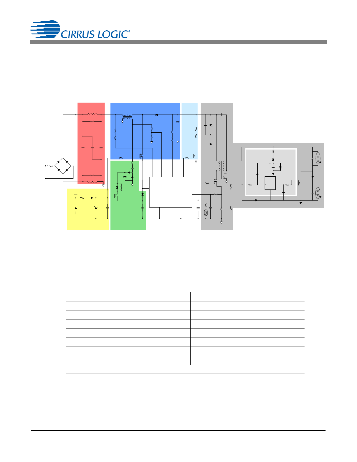
Figure 1. Diagram of CS1630 Design
Driving Two LED Strings in Series
3 Design Process
The design process for a two-stage power converter system can be partitioned into seven circuit blocks (see
Figure 1). The AC line voltage is passed through an electromagnetic interference (EMI) filter to prevent injection of
switching noise from the driver into the power line. The output of the EMI filter is then converted to the desired DC
output by a boost PFC followed by a flyback converter. The second stage is an isolated flyback circuit that requires
a phase synchronizer to control the two-channel output currents. The power converter system includes the Gate Bias, Steady State Supply, and Active Clamp support circuitry.
3.1 Operating Parameters
To initiate the design procedure, a set of operating parameters is required. Operating parameters required for
the analytical process are outlined in the table below. Parameters critical to the overall design, but not
specifically addressed in this document, include EMI compliance, efficiency, form factor, layout, and operating
temperature.
Parameter Symbol
Output Power
AC Line Input Voltage
Channel 1 Secondary Output Voltage
Channel 2 Secondary Output Voltage
Channel 1 Load Current
Channel 2 Load Current
Maximum Switching Frequency*
* Increasing Fsw may reduce the size of the magnetics but increases switching losses in the FET.
AN368REV2 9
P
OUT
V
IN
V
CH1
V
CH2
I
CH1
I
CH2
F
sw(max)
Page 10

3.2 Design Process
The design process requires a specification covering the required operating range, color temperature, dimmer
compatibility, form factor, and applicable standards. Once those specifications are defined, the recommended
design process is as follows:
Design the Flyback Stage
• Define power-stage components, such as the MOSFET and zener clamp, based on certain considerations,
including cost, performance, and space
• Calculate transformer parameters and remaining power-stage components
• Design transformer based on cost, size, and performance
• Design Synchronizer Circuit
• Specify protection thresholds
Design the Color System
Perform curve fit that meets target specifications for color and lumen output across the dimming range
Design the Boost Stage
• Pick power semiconductors for the boost stage based on input power required by flyback and nominal link
voltage
• Determine peak current in the boost stage during No-dimmer Mode
• Boost inductor design based on providing best-case tradeoff between efficiency, EMI, and size of
magnetics
AN368
Design of the Other Non-power Conversion Circuitry
• Design charge pump, auxiliary supply circuit for providing V
• Clamp circuit
Design the EMI Filter
• Design EMI filter to meet required compliance
Design Other Protections
• ZCD
• OCP, OLP, OVP, VDIFF, BOP, COP, LLP
• eOTP, iOTP
Layout the PCB
• Observe GND rules
• Sensitive traces
Optimize Output Regulation of Flyback Section
• Correct for actual ZCD offsets
• Compensate T2 commutation time
• I
Program the Device
• OTP memory
• Compute CRC
• OTP Verification
(T1) compensation
PK(FB)
to the IC
DD
Optimize EMI Filter
• Verify EMI filter meets dimmer compatibility
• Optimize EMI filter for compliance
10 AN368REV2
Page 11
3.3 Design Procedure
D2
R22
Z3
R21
R23
Q5
CS1630 /31
FBAUX
GND
13
GD
FBSEN SE
15
12
11
TX1
V
BST
R3
D6
U2
C10
C8
C15
D5
D
GND
_
Q
VCC
D15
R12 D10
Q3
R2
C16
Channel 1 LED
(White)
Channel 2 LED
(Red)
GND
IGND
I
MODE x
I
PRI
V
MODE x
D9
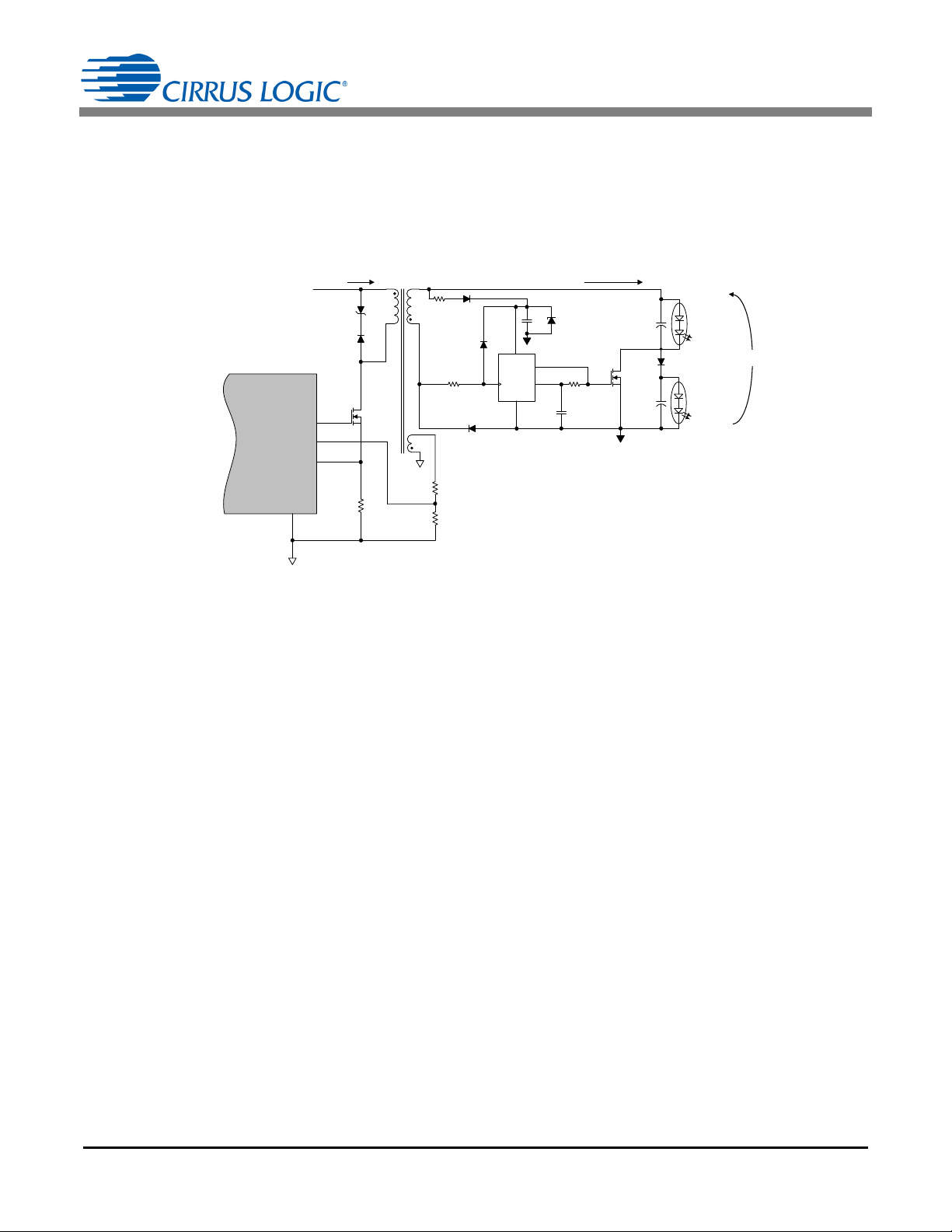
Figure 2. Flyback Series Output Model
Step 1) Select Input Voltage
The CS1630 is optimized for 120VAC line voltage applications and designs targeting 108 to 132 VAC markets.
Step 2) Design for a Flyback Topology
The light engine is defined for a flyback topology in a series configuration. Figure 2 illustrates a flyback
topology with a series lamp configuration.
AN368
This document focuses on designing and programming a driver with a flyback topology in a series
configuration. Cirrus Logic, Inc. and its affiliates and subsidiaries generally make no representations or
warranties that the combination of Cirrus Logic’s products with light-emitting diodes (“LEDs”), converter
materials, and/or other components will not infringe any third-party patents, including any patents related to
color mixing in LED lighting applications, such as, for example, U.S. Patent No. 7,213,940 and related patents
of Cree, Inc. For more information, please see Cirrus Logic’s Terms and Conditions of Sale, or contact a Cirrus
Logic sales representative.
a. Set OTP for a Series Configuration
The two LED strings are arranged in series so that current passes through either one or both LED strings. A
MOSFET is used to shunt current around one string on alternating switching cycles. In this configuration, one
string is required to have a larger output current than the other string.
When considering a series design, it is recommended that the current flowing through one of the LED channels
be 80% or lower than that of the other LED channel at all times. The LED string that has current flowing
continuously is referred to as channel 1 LED (I
channel 2 LED (I
CH2
); I
CH2
0.8I
. A good rule of thumb is that channel 2 LED must always have a forward
CH1
), while the string with the bypass FET is referred to as
CH1
voltage of 85% or lower than channel 1 LED.
The LED_ARG bit in register Config3 at Address 35 selects which channel is connected to the color LED string.
When bit LED_ARG is set to ‘1’, the color LED string is connected to channel 2.
The STRING bit in register Config3 at Address 35 selects the second-stage output channel configuration.
When bit STRING is set to ‘1’, a series configuration is selected.
b. Selecting a Flyback Topology
Flyback topology is enabled by setting bit S2CONFIG to ‘1’ in register Config12 at Address 44. The flyback
transformer input-to-output voltage ratio is used to determine the duty cycle and minimum turn ‘ON’ switching
period T1 for the power FET. The flyback transformer is designed as an isolated topology, and the digital
synchronization signal needs to be disabled. Set bit SYNC in register Config4 at Address 36 to ‘0’. Since bit
S2CONFIG is configured for a flyback topology, bits BUCK[3:0] in register Config10 at Address 42 are ignored
by the digital algorithm.
AN368REV2 11
Page 12
Step 3) Determine Second-stage Parameters for a Flyback Topology
Steps for the Flyback Design
1. Set the boost output voltage, V
BST
.
2. Select a MOSFET that aligns with the quality standards
of the designer’s company.
3. Determine the transformer turns ratio from the
V
BST
, FET
voltage, and reflected voltage, V
Reflected
.
4. Use the nominal switching frequency and an initial
estimate for time T3 to determine the value of time TT at
full brightness.
5. Use V
BST
, TT, and V
Reflected
to determine time T1 and
T2.
6. Use time T2 and TT, turns ratio N, and load current to
determine the value of the peak primary current, I
PK(FB)
.
7. Use I
PK(FB)
to determine R
Sense
.
8. Calculate the primary-side inductance using time T1.
9. Calculate flyback gain resistor R
FBGAIN
using full load
conditions. Ensure linearity of the load versus the dim
curve.
10. Calculate primary and secondary RMS currents using
I
PK(FB)
and duty cycle.
11. Select an output capacitor.
12. Determine the flyback transformer specifications.
13. Determine if the flyback transformer fits into specified
form factor after designing and constructing flyback
transformer. Repeat steps 3 to 12 until form factor
criteria is met.
14. Refinements to the circuit with final flyback transformer
design.
15. Validate that the system meets the operating criteria.
Second Stage
Flyback Specifications
Determine N, Fsw,
V
Reflec ted
, and V
CLAMP
Estimate T3
Calculate TT
fb
Calculate R
Sense
,
R
FBG AIN
, and Primary
Inductance
Color System
Parameters
Fit?
Yes
No
Calculate T1,
T2, and I
PK(FB)
Calculate RMS Current
and Output Capacitor
Transformer Core
Figure 3. Flyback Stage Design
Figure 3 illustrates the steps for designing the second stage.
AN368
12 AN368REV2
Page 13

AN368
V
Drain maxVBST maxVZener max
+=
[Eq. 1]
V
Overshoot
V
ZenerVReflecteed
–=
[Eq. 2]
V
Margin
V
Zener
V
BST
V
Overshoot
V
Reflected
F
ET Breakdown
Voltage Rating
Clamp
Zener
Voltage
Boost Output
Voltage
Margin
Reflected
Voltage
Overshoot
Voltage
Overshoot is a brief condition above
V
Reflected
, required to quickly dissipate
the energy stored in the transformer
leakage inductance.
During this time, the primary current is
kept from transferring to the secondary, siphoning energy from the load to
the clamp zener (snubber).
Figure 3. FET Breakdown Voltage
a. Set the Value for Boost Output Voltage
The value of the boost output voltage V
maximum V
voltage V
BST
BST(max)
should be kept as low as possible to help keep the FET breakdown
requirement within economical constraints.
V
is determined by an internal parameter and changes slightly depending on the type of dimmer detected.
BST
With sense resistors R13, R14, R17, and R18 set to 750k each, the resulting V
for a 120V system. V
line-cycle. V
droops to its lowest value towards the end of each half line-cycle until the boosting process
BST
is regulated by charging the boost output capacitor to its nominal value each half
BST
starts again in the next half line-cycle.
b. Select an Appropriate FET
Determine the FET Q5 breakdown voltage V
drain voltage V
Drain(max)
is calculated using Equation 1.
The ringing associated with the transformer leakage inductance usually does not have enough energy to
cause a destructive avalanche breakdown. Voltages closely approaching the FET breakdown voltage are
acceptable. Alternatively, V
should be much greater than V
Zener
in the transformer leakage inductance.
The FET breakdown voltage is constrained by cost and performance. A compromise must be reached in
partitioning voltage between V
V
Zener
into V
Reflected
and a reasonable overshoot voltage portion, V
BST
, V
The losses caused by the leakage inductance are inversely proportional to V
Equation 2.
must be greater than the maximum input AC line voltage peak. The
BST
is approximately 200 V
BST
Zener
Breakdown
, and V
and reflected voltage V
Reflected
. A second compromise then determines how to divide
Margin
to rapidly discharge the energy stored
Overshoot
Reflected
.
Overshoot
. The FET maximum
, which is determined by
AN368REV2 13
Page 14
AN368
[Eq. 3]
V
Breakdown
V
BST maxVZenerVMinarg
++=
N
V
Reflected
V
CH1 maxVCH2 max
+
--------------------------------------------------------------
=
[Eq. 4]
i(t)
T1
CH1
T2
CH1
TT
CH1
No Current
T3
CH1
Secondary
Current
t
T1
CH2
T2
CH2
No Current
T3
CH2
Secondary
Current
TT
TT
CH2
Peak Primary Current 2, I
PK2(FB)
Primar y
Current
Peak Primary Current 1, I
PK1(FB)
Primar y
Current
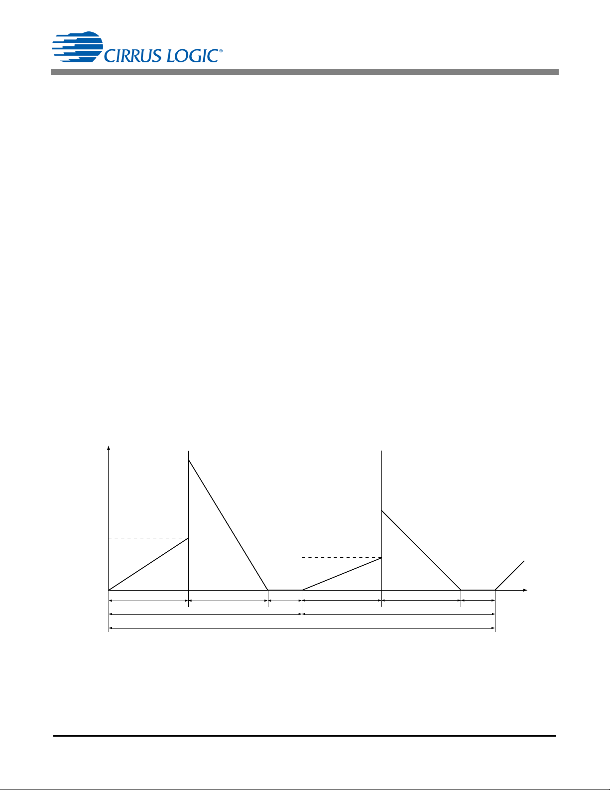
Figure 4. Timing Diagram for Switching Frequencies
1
F
sw max
---------------------
TTFREQ[7:0] 4 50ns=
[Eq. 5]
For optimum efficiency, the increase in transformer losses (created by an uneven duty cycle) must balance the
reduction of the losses caused by discharging the leakage inductance (obtained by increasing the overshoot
voltage). Equation 3 is used to balance all voltages contributing to the FET voltage drain and source.
where,
V
Overshoot
c. Determine the Flyback Transformer Turns Ratio
Select a turns ratio based on the channel output voltage, V
where,
V
CH1(max)
V
CH2(max)
d. Select the Full Brightness Switching Frequency
The CS1630 has two switching events with frequencies F
frequency F
1. Maximum channel-switching frequencies F
2. Maximum flyback stage switching frequency F
3. For EMI considerations, the higher switching frequency between the two channels should be less than
4. Switching frequency F
5. Switching frequencies F
= V
Zener
- V
Reflected
= Maximum channel 1 LED forward voltage V
= Maximum channel 2 LED forward voltage V
. Common criteria for determining the desired switching frequency include:
sw
sw1(max)
75kHz.
should be in audible range only at low power.
sw
sw1
and F
are selected such that the size of the flyback transformer meets
sw2
the converter system form factor requirements.
, V
CH1
at full current plus the rectifying diode voltage VF.
CH1
at full current plus the rectifying diode voltage VF.
CH2
and F
sw1
and F
sw2(max)
is less than 100kHz.
sw(max)
, and V
CH2
sw2
Reflected
that make up a complete switching
, using Equation 4.
are less than 200kHz.
14 AN368REV2
The maximum switching frequency F
Address 46. Bits TTFREQ[7:0] set the minimum allowable target period for the second-stage time TT:
sw(max)
for the second stage is configured using the TTFREQ register at
Page 15

AN368
1
F
sw min
--------------------
TT MAX[7:0] 128 127+50ns= [Eq. 6]
V
MODE1
V
CH1VCH2VD15VD5
+++=
[Eq. 7]
I
MODE1ICH2
=
[Eq. 8]
V
MODE2
V
CH1VD15
+=
[Eq. 9]
I
MODE2ICH1ICH2
–=
[Eq. 10]
The minimum switching frequency F
for the second stage is configured to provide good power
sw(min)
regulation. The minimum switching frequency should be set to the smallest possible value, but it should remain
outside of the audible frequency range. F
is configured using register TTMAX at Address 38. Bits
sw(min)
TTMAX[7:0] set the maximum allowable target period for the second-stage time TT:
The maximum second-stage switching period that is measured by the controller algorithm is set using bits
TT_MAX[1:0] in register Config3 at Address 35.
TT_MAX[1:0] Max Switching Period
0 51.15s
1 102.35s
2 153.55s
3 204.75s
Table 1. Maximum Measurable Switching Period
There are two modes of operation, and the output configuration in each of these modes is different.
Mode 1: Switching Event TT
In Mode 1 the phase synchronizer FET Q3 is switched ‘OFF’. Output voltage V
I
are calculated using Equations 7 and 8, respectively:
MODE1
CH1
and output current
MODE1
where,
V
= Channel 1 secondary output VDC (channel 1 LED string supply voltage)
CH1
V
= Channel 2 secondary output VDC (channel 2 LED string supply voltage)
CH2
V
= Forward bias voltage across diode D15
D15
V
= Forward bias voltage across diode D5
D5
I
= Channel 2 LED current
CH2
Mode 2: Switching Event TT
In Mode 2, phase synchronizer MOSFET Q3 is switched ‘ON’. Output voltage V
I
are calculated using Equations 9 and 10, respectively:
MODE2
CH2
and output current
MODE2
where,
I
= Channel 1 LED current
CH1
e. Determine the Flyback Nominal Timing T1 and T2
Assume that the power transferred in Mode 1 is greater than the power transferred in Mode 2. Select a Mode 1
switching frequency F
for optimal driver performance using the criteria described above.
sw1
AN368REV2 15
Page 16

AN368
[Eq. 11]
D
MODE1
NV
MODE1
V
BST
NV
MODE1
+
----------------------------------------------------------
=
[Eq. 12]
D
MODE2
NV
MODE2
V
BST
NV
MODE2
+
----------------------------------------------------------
=
TT
CH1
T1
CH1
T2
CH1
+
1
F
sw1
-----------
==
[Eq. 13]
F
sw2
F
sw1
V
BST
NV
MODE1
+
V
BST
NV
MODE2
+
----------------------------------------------------------
I
MODE1VMODE2
I
MODE2VMODE1
------------------------------------------
=
[Eq. 14]
TT
CH2
T1
CH2
T2
CH2
+
1
F
sw2
-----------
==
[Eq. 15]
TT
CH1
T= 1
CH1
T2
CH1
T3
CH1
++
[Eq. 16]
TT
CH2
T= 1
CH2
T2
CH2
T3
CH2
++
[Eq. 17]
TT TT
CH1
TT
CH2
+=
[Eq. 18]
F
sw
1
TT
-------
=
[Eq. 19]
[Eq. 20]
T1
CH1
TT
CH1
T3
CH1
–D
MODE1
=
[Eq. 21]
T1
CH2
TT
CH2
T3
CH2
–D
MODE2
=
Calculate Mode 1 duty ratio D
Assuming the resonant times T3
and Mode 2 duty ratio D
MODE1
and T3
CH1
CH2
using Equations 11 and 12, respectively:
MODE2
are zero, the remaining relevant flyback stage parameters can
be calculated using the turns ratio N calculated in Equation 4 and the switching frequency F
Mode 1. Calculate period TT
Calculate switching frequency F
Calculate period TT
using Equation 15:
CH2
using Equation 13:
CH1
using Equation 14:
sw2
selected for
sw1
The resonant times T3
CH1
and T3
are estimated for both channels. Deriving a more accurate value of the
CH2
resonant ringing time is discussed in Step 4g Automated Resonant Period Measurements on page 22. To
account for times T3
periods TT
CH1
and TT
and T3
CH1
using Equations 16 and 17, respectively.
CH2
that were neglected in the first approximation of Equation 13, recalculate
CH2
Calculate total period TT using Equation 18:
Calculate switching frequency Fsw using Equation 19:
Calculate the MOSFET ‘ON’ time T1
Calculate the MOSFET ‘ON’ time T1
in Mode 1 using Equation 20:
CH1
in Mode 2 using Equation 21:
CH2
16 AN368REV2
Page 17

AN368
[Eq. 22]
T2
CH1
TT
CH1
T1
CH1
– T3
CH1
–=
[Eq. 23]
T2
CH2
TT
CH2
T1
CH2
– T3
CH2
–=
[Eq. 24]
L
P
N2V
BST
2
V
MODE1
2V
BST
NV
MODE1
+
2
I
MODE1
TT F
sw1
2
-----------------------------------------------------------------------------------------------------------------------
=
[Eq. 25]
I
PK1 FBVBST
T1
CH1
L
P
----------------
=
[Eq. 26]
I
PK2 FBVBST
T1
CH2
L
P
----------------
=
[Eq. 27]
I
MODE1 avgIPK1 FB
N
T2
CH1
2TT
----------------
=
[Eq. 28]
I
MODE2 avgIPK2 FB
N
T2
CH2
2TT
----------------
=
[Eq. 29]
I
PRI RMSIPK1 FB
2
D
MODE1
3
--------------------
I
PK2 FB
2
D
MODE2
3
--------------------
+=
Calculate the MOSFET ‘OFF’ time T2
Calculate the MOSFET ‘OFF’ time T2
in Mode 1 using Equation 22:
CH1
in Mode 2 using Equation 23:
CH2
f. Calculate the Flyback Primary-side Inductance
Calculate the flyback transformer primary-side inductance L
g. Calculate Peak Current on the Flyback Primary-side
Calculate peak current I
Calculate peak current I
PK1(FB)
PK2(FB)
during Mode 1 using Equation 25:
during Mode 2 using Equation 26:
using Equation 24:
P
Calculate the average current I
Calculate the average current I
MODE1(avg)
MODE2(avg)
during Mode 1 using Equation 27:
during Mode 2 using Equation 28:
Equations 27 and 28 inherently assume that the IC generates the exact value for the FET ‘OFF’ time and the
peak currents. In practice, this is not always true due to the presence of parasitics in the system that cause
differences between the theoretical and measured value of peak current I
and time T2. Step 5 Optimize
PK(FB)
Output Current Regulation on page 24 describes in detail the way the CS1630 can compensate for these
differences.
h. Determine the RMS Current in the Winding
The CS1630 has a minimum required period T1 calculated in Equations 20 and 21 that is dependent on the
leading-edge blanking time T
. Blanking time T
LEB
is programmable from 150ns to 800ns and is used to
LEB
effectively disable the peak current comparator from turning off the gate drive too early due to spurious
switching noise. In applied systems, a good rule of thumb is to target a minimum duty cycle of 10% or greater.
The RMS current in the primary winding I
PRI(RMS)
is calculated using Equation 29:
AN368REV2 17
Page 18
AN368
[Eq. 30]
I
SEC RMS
N2I
PK1 FB
2
1D
MODE1
–
3
-----------------------------
N
2
I
PK2 FB
2
1D
MODE2
–
3
-----------------------------
+=
[Eq. 31]
R
Sense
1.4V
f
scale
I
PK1 FB
-------------------------------------=
[Eq. 32]
P
SenseIPRI RMS
2
R
Sense
=
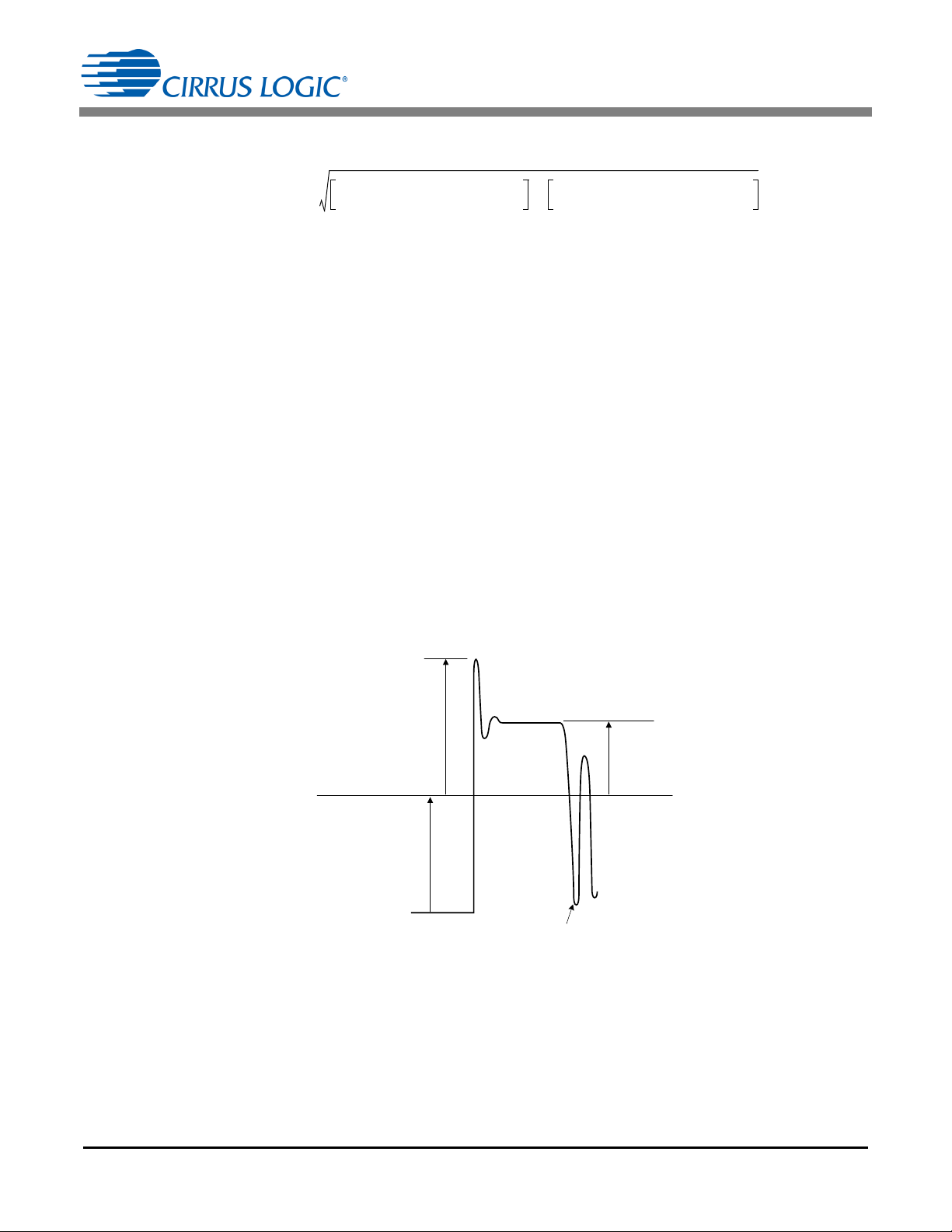
Fir st Valley
Flyback FET
Voltage
V
CLAM P
V
BST
V
Reflected
Figure 5. Switching Waveform of Flyback FET Drain
[Eq. 33]
N
P
N
FBAUX
-------------------
2NV
OVP
R23
1.25V R22 R23+
------------------------------------------------------
=
The RMS current in the secondary winding I
i. Calculate R
Sense
(R21)
SEC(RMS)
is calculated using Equation 30:
A scaling factor is used to provide for a margin to account for manufacturing tolerances of external
components, such as inductance and resistance tolerance. Calculate sense resistor R
(R21) for flyback
Sense
using Equation 31:
where,
f
= Scaling factor
scale
R21 = R
Calculate the power P
Sense
in
dissipated by the sense resistor R
Sense
(R21) using Equation 32:
Sense
j. Calculate Flyback Zero-current Detection
The CS1630 uses zero-current detection (ZCD) to minimize switching losses. The ZCD algorithm is designed
to turn ‘ON’ the flyback FET Q5 when the resonant voltage across the FET is at a low point (see Figure 5).
Valley switching reduces the CV
2
power losses associated with the body capacitance of the FET. Pin FBAUX
is designed to monitor the resonant voltage from the auxiliary winding of the flyback transformer T1.
The auxiliary turns ratio must be designed such that the output voltage from the auxiliary winding is attenuated
by a resistor voltage divider that results in a 1.25V input to the FBAUX pin when the OVP threshold V
reached. In addition, the total current through the ZCD circuit should be limited to less than 1mA. The
transformer TX1 auxiliary winding turns ratio
is calculated using Equation 33:
OVP
is
18 AN368REV2
Page 19

AN368
[Eq. 34]
l
g
0.5 oL
P
I
PK1 FB
2
B
PK
2
Ae
--------------------------
=
[Eq. 35]N
P
L
P
I
PK1 FB
BPKAe
---------------------
=
N
S
N
P
N
-------
=
[Eq. 36]
The FBAUX pin current must be limited to less than 1mA. Resistor R22 plus resistor R23 should be chosen
such that current V
resistor of at least 22k must be used to limit the current. Bit VALLEYSW in register Config2 at Address 34
configures the quasi-resonant switching (valley switching) on the second stage. To enable valley switching,
set bit VALLEYSW to ‘1’. Bit POL_ZCD in register Config4 at Address 36 configures the polarity of the zerocurrent detection comparator output. It is recommended to set the ZCD comparator output to active-low by
setting bit POL_ZCD to ‘0’.
k. Determine Output Capacitors
The flyback output capacitors must provide a low impedance to the switching frequency. When using an
electrolytic capacitor, the choice is based on its ability to carry the ripple current so that it provides a long
service life. A capacitor that fulfills the ripple, voltage, temperature, and life requirements results in a capacitor
with a large capacitance that is often much greater than what is necessary to smooth the load current. In
flyback applications, the voltage ripple across the output electrolytic capacitor is determined mostly by the ESR
rather than the reactance.
l. Flyback Transformer Design
The following information is now available:
1. Maximum peak currents through the primary
2. Inductance
3. Turns ratio
4. RMS current through the winding
The core can be chosen using the transformer core data sheet, K
selecting the core, the gap and the number of turns can be calculated using Equations 34, 35, and 36.
The air gap length l
/(R22 + R23) is less than 1mA during the time when FET Q5 is ‘ON’ or ‘OFF’. A series
AUX
constant, or the area product. After
g
is calculated using Equation 34:
g
where,
= Permittivity of free space = 4 x 10⁻⁷ H/m
o
A
= Effective cross-sectional area of the core in mm
e
2
BPK = Peak flux density in Tesla
L
= Primary inductance in Henry
P
The primary turns N
The secondary turns N
Both N
and NP have to be an integer. Therefore, the actual flyback transformer turns ratio N may be
S
is calculated using Equation 35:
P
is calculated using Equation 36:
S
marginally different from the theoretical calculations. Hence the inductance needs to be re-calculated in order
to maintain the desired frequency spectrum. Circuit adjustments are required after the transformer has been
designed and constructed. Optimum efficiency, at full brightness, is obtained when the system is switching as
close to CRM as possible and turning on the first valley as illustrated in Figure 5. The ZCD delay can be
adjusted to hit the valley accurately, and this is demonstrated in Step 5b Tune Flyback ZCD Fixed Delays for
Optimum Valley-switching Performance on page 25.
AN368REV2 19
Page 20

AN368
CHxCUR
511 2 R
SenseICHx
NV
Sense
-------------------------------------------------------
=
[Eq. 37]
[Eq. 38]
T
LEB
LEB[3:0]= 2 50ns
m. Recalculate R
The flyback primary current is controlled by comparing the voltage across R
Sense
at pin FBSENSE to an
Sense
internal threshold of 1.4V. To guarantee the rated LED current under worst-case conditions, when the LED
string has maximum voltage, the V
R
to obtain the nominal LED current using Equations 31 and 32.
Sense
Once the current sense resistor R
is at its minimum point and R
BST
value is determined, the target output current CHxCUR for the channel
Sense
is at its highest tolerance. Adjust
Sense
can be calculated using Equation 37:
where,
V
= Voltage across sense resistor
Sense
I
= Current thought LED string
CHx
The target output current CHxCUR corresponds to a 9-bit OTP value and is programmed by bit CH1CURMSB
in register Config8 at Address 40 plus bits CH1CUR[7:0] at Address 41 for channel 1 and bit CH2CURMSB in
register Config10 at Address 42 plus bits CH2CUR[7:0] at Address 43 for channel 2.
Step 4) Tune Second-stage Performance and Limiting Parameters
The CS1630 LED controller provides a number of configurable parameters for controlling features of the
second-stage control. These features include leading- and falling-edge blanking times, configurable
deglitching of comparator outputs, dithering, resonant period probing, and phase synchronization. The optimal
values for many of the OTP general parameters not concerned with specific output design parameters have
been determined experimentally to cover the broadest design approaches. Unless there is a reason to change
them, these parameters are best set at their default values.
a. PID Feedback Controller
The maximum coefficient for the second-stage PID integrator is configured using register PID at Address 45.
The recommended value for a flyback topology that should be programmed in the PID register is ‘00000010’.
Bits RSHIFT[3:0] in register Config8 at Address 40 set the number of right shifts performed on the secondstage PID integrator value to generate a 10-bit threshold value for the peak control comparator. For peak
rectify mode, the threshold is calculated by a right shift of the integrator value. For example, setting
RSHIFT[3:0] to 12, the 24-bit integrator is shifted right 12 times, and the remaining bits represent the threshold
value provided to the peak control comparator. The recommended value that should be programmed in
RSHIFT[3:0] is ‘1100’.
b. Leading-edge Blanking
Configurable blanking time on the I
comparator provides protection to suppress potential false
Sense
comparator values caused by spurious noise induced by the power FET switching at the rising edge of the gate
drive. The controller ignores output from the comparator from the rising edge of the gate drive to the end of the
blanking time interval. The duration of the leading-edge blanking time T
is set using the LEB[3:0] bits in
LEB
register Config18 at Address 50.
A setting of LEB[3:0] = 2 results in a leading-edge blanking time of 200ns. In addition, the leading-edge
blanking sets the minimum gate drive duration or T1 time for the design. Since the I
comparator is ignored
Sense
during the leading-edge blanking time, the gate drive remains asserted throughout the leading-edge blanking
time.
20 AN368REV2
Page 21

AN368
[Eq. 39]
T
TEB
TEB[3:0]= 2 50ns
[Eq. 40]
T1
max
GD_DUR 87+= 50 ns
[Eq. 41]
V
IPK min
1.4
IPEAK[2:0] 1+1615+CL AMP[1:0] 8– 8 +
512
---------------------------------------------------------------------------------------------------------------------------------------------------
=
c. Trailing-edge Blanking
Configurable blanking time on the zero-current detection (ZCD) comparator provides protection to suppress
false comparator values due to noise at the falling edge of the gate drive. The controller suppresses any
comparator result from the falling edge of the gate drive to the end of the configurable trailing-edge blanking
time. The duration of the trailing-edge blanking time is set through the TEB[3:0] bits in register Config18 at
Address 50.
A setting of TEB[3:0] = 5 results in a trailing-edge blanking time of 500ns. In addition, the trailing-edge blanking
sets the minimum T2 time for the design since the ZCD comparator is ignored during the trailing-edge blanking
time.
d. Maximum Gate Drive Duration
The CS1630 controller provides configurable maximum gate duration to protect against a potential overstress
condition. The gate drive to the power FET is automatically disabled if the gate drive duration exceeds the
configurable limit in the absence of a trip of the I
T1
is configurable using the GD_DUR register at Address 33.
max
A setting of 65 for register GD_DUR provides a maximum gate drive duration time of 26.35s. The GD_DUR
register can be set to a percentage over the gate drive duration expected for the maximum peak current within
the system.
e. Minimum Measurable Peak Current
To achieve optimum output regulation at low dim values, the minimum measurable peak current must be set.
Voltage V
IPK(min)
corresponds to the minimum peak current measurement across sense resistor R
FET Q4 is turned ‘ON’ and is calculated using the minimum peak current level bits IPEAK[2:0] in register
Config3 at Address 35 and the offset adjustment bits CLAMP[1:0] in register Config2 at Address 34.
comparator output. The maximum gate drive duration
Sense
Sense
when
Setting the voltage V
V
IPK(min)
to be less than 0.2V can increase sensitivity to noise leading to a jittery control. For the CS1630,
IPK(min)
to be greater than 0.7V reduces the range of output regulation. Setting the voltage
0.25V should be considered the lower limit. For the CS1631, 0.35V should be considered the lower limit.
f. T2 Time-out Configuration
The CS1630 controller provides a T2 time out limit to ensure a minimum switching frequency for each channel.
The T2 duration is measured from the falling edge of the gate drive to the time at which the secondary current
equals zero. The controller uses the ZCD comparator output to locate the end of the T2 duration. If the T2
duration exceeds the T2 time out limit, the current switching cycle is terminated, and the gate drive for the next
channel switching cycle initiates.
The T2 time out limit is configurable through the TIMEOUT[1:0] bits in register Config12 at Address 44.
TIMEOUT[1:0] T2 Time-out Limit
045ms
170.6ms
296.2ms
3 121.8ms
Table 2. T2 Time-out Limits
AN368REV2 21
Page 22
AN368
T
RES
Figure 6. Waveforms of the Resonant Frequency
[Eq. 42]
TT
Cycles
16 P RCNT[3:0]15+=
[Eq. 43]
T
RES
4
---------------
2 PRCNT[3:0] 50ns=
g. Automated Resonant Period Measurements
To ensure accuracy of the T2 duration measurements within the CS1630 controller, the resonant period T
of the power train can be automatically measured during the T3 time (secondary current equals zero) of the
switching cycle. To enable the automated resonant period measurement, set the PROBE bit within register
Config7 at Address 39 to a value of ‘1’. To measure the resonant period, the controller forces DCM operation
at selected multiples of TT and measures the duration between the first and second zero-crossing detections.
RES
The frequency of the automated resonant period measurements is configurable through the PRCNT[3:0] bits
in register Config7 at Address 39. The number of channel 1 switching cycles TT
between resonant period
Cycles
measurements is set by Equation 42.
To force a resonant period measurement every 47 switching cycles, TT
, a value of 2 is programmed into
Cycles
the PRCNT[3:0] bits.
If the automated resonant period measurement is not desired, the controller supports the option to manually
program the resonant period. In this case, the PROBE bit is disabled with a value of ‘0’, and the value of onequarter of the resonant period T
If the resonant period T
is 800ns, a value of ‘2’ is programmed into bits PRCNT[3:0].
RES
is programmed using the PRCNT[3:0] bits in Equation 43.
RES
22 AN368REV2
Page 23
AN368
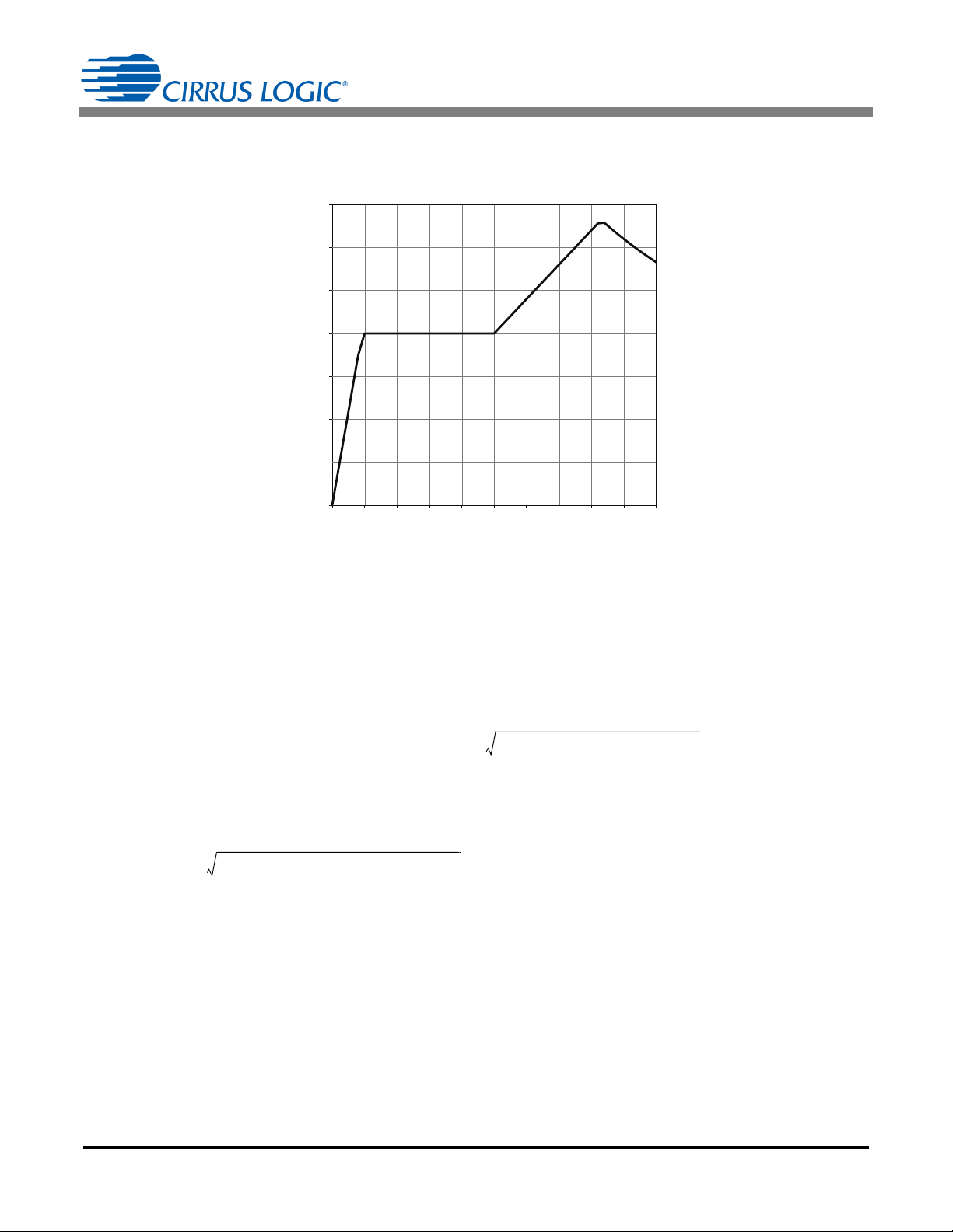
0
5
10
15
20
25
30
35
0.10 0.20 0.30 0.40 0.50 0.60 0.70 0.80 0.90 1.00
Frequency (kHz)
Dim
D
C
B
A
Figure 7. Dual Pulses Switching Frequency
TT
A
0.5 TT
dim1
TT
dim2
+ TT
dim1
TT
dim2
+
2
4T
res
++
2
=
[Eq. 44]
TT
dimx
2LdimI
MODEx
N2V
MODEx
1D
MODEx
–=
[Eq. 45]
TT
B
TT
FREQ
dim
--------------------
=
h. Switching Frequency Across Dim Range
From the equations below and setting the OTP registers as follows, the switching frequency across the dim
range can be calculated. A sample plot of the switching frequency across dim values is shown in Figure 7.
The frequencies in regions A, B, C, and D are governed by Equations 44, 45, 46 and 47, respectively.
Transitions between connecting regions are the result of simple inequalities. The following four equations do
not include the effect of a color system. Equations 44 through 47 must be adjusted after the color system has
been designed.
Frequency in Region A
In Region A, the system operates in CRM, and the period TT
is calculated using Equation 44:
A
where,
> TTB at the given dim level
TT
A
dim = The 12-bit dim level provided by the boost stage
Frequency in Region B
In Region B, the system operates in DCM, but the peak current remains the same. Period TT
using Equation 45:
where,
TT
< 50s
B
TT
> TT
B
A
is calculated
B
AN368REV2 23
Page 24

AN368
[Eq. 46]
TT
C
50s=
[Eq. 47]
TT
D
TT
DCM_2IPK min
2
L
2dimI
MODExVMODEx
-----------------------------------------------------------------
==
[Eq. 48]
I
CH1
I
CH1 fb
dim
4095
---------------------------------
=
I
CH2
I
CH2 fb
dim
4095
---------------------------------
=
[Eq. 49]
Frequency in Region C
In Region C, the switching frequency is kept constant, and the peak current I
TT
is calculated using Equation 46:
C
Frequency in Region D
Once the peak current I
reaches its minimum value, the switching frequency continues to reduce until
PK(FB)
the minimum peak current limit is reached, or the minimum switching frequency set by the maximum switching
period register TTMAX at Address 38. The period TT
is calculated using Equation 47:
D
where,
I
PKx(FB)
= I
PK(min)
TTD > TTC (50s)
TT
< TTMAX
D
starts to reduce. Period
PK(FB)
If the operating frequency is below TTMAX, the system stops regulating because the controller is out of range
to control the current I
PKx(FB)
or the frequency.
Step 5) Optimize Output Current Regulation
The CS1630 second-stage control loop achieves correct closed-loop output current regulation based on
measured values of time T1, current I
, and time T2. In practical systems, accurate measurements are
PK(FB)
limited due to circuit parasitics. Examples of circuit parasitics are leakage inductance, inter-winding
capacitance, and diode recoveries. The controller has the ability to compensate for these measurement errors
so that the control loop can maintain a tight current regulation across the corners. The following steps describe
the process of tuning these compensations accurately to minimize conversion error.
a. Definition and Scope of Second-stage Output Current Regulation
In a system where all the CS1630 second-stage compensation features have been tuned correctly and the
color system is disabled (for example, GAIN
and GAIN
DR
are forced to 1), the output current on the two
DTR
channels scales perfectly with the 12-bit dim level provided by the boost stage using Equations 48 and 49.
where,
dim = The 12-bit dim level provided by the boost stage
I
= Current at full brightness, when the dim is 4095 (full scale) provided that the color system is disabled
CH1(fb)
24 AN368REV2
Page 25

AN368
I
error
I
calculateImeasure
–
I
calculate
----------------------------------------------
100
=
[Eq. 50]
The linearity of the second-stage current regulation is determined by the error between the expected currents
at any given dim level and the measured currents at that dim level. Percentage error I
is given by Equation 50:
where,
I
calculate
I
measure
= Current calculated in Equation 48 and 49
= Current measured at dim level
If this error is zero across the operable system dim range, which may be from 2% to full brightness, the second
stage has ideal linear output current regulation. Note that this error definition does not include the errors due
to curve fitting the target color system. It is recommended to optimize the second stage first using this section
so that the remaining margin of error for the overall system output regulation is understood when the color
system is enabled.
b. Tune Flyback ZCD Fixed Delays for Optimum Valley-switching Performance
To minimize switching losses, the valley-switching performance needs to be optimized using the following
steps:
1. Probe the drain voltage of the second-stage FET so that the drain voltage resonant ringing can be
observed when the T2 time is over. Also probe the FBAUX pin on the IC. The two waveforms should be
similar, with the FBAUX voltage waveform being a phase-delayed and scaled-down version of the drain
voltage minus the DC boost output voltage V
component (see Figure 5).
BST
2. The internal ZCD comparator has a reference of 200 mV. If the ringing waveforms at the end of time T2
are greatly attenuated so that resonant voltage is barely above 200 mV, the device comparator will not
be able to detect the zero crossings on the signal applied to the FBAUX pin.
3. Automatic T
RES
probing:
i. For the IC to automatically measure the resonant frequency and use it for valley switching, enable
the PROBE bit within register Config7 at Address 39. Set the probe count PRCNT[3:0] bits in register Config7 at Address 39 to obtain the desired probing frequency. It is recommended to leave this
setting at its max value initially. The automatic probing cycles can be viewed by setting the system
at a full dim level where it is always switching in CRM mode. The switching cycles that show more
than one valley are the T
cycles, where TT
is proportional to the probe count PRCNT[3:0] bits.
N
probe cycles. These should occur after every TTN number of switching
RES
ii. To disable resonant frequency probing and specify a fixed resonant period value, the PROBE bit
within the Config7 register can be disabled and the quarter resonant period can be set by steps of
100ns using the probe count PRCNT[3:0] bits in the Config7 register (see Equation 43).
4. Set bits CH1_ZCD[2:0] in register Config8 at Address 40 and bits CH2_ZCD[2:0] in register Config16
at Address 48 to ‘0’. These settings are used to account for the various path delays involved in between
the V
crossing time at the drain voltage and the ZCD comparator tripping.
BST
5. Set the system to full brightness so that it is in CRM mode. The valley-switching point for each channel
can be tweaked independently using bits CH1_ZCD[2:0] in the Config8 register and bits CH2_ZCD[2:0]
in the Config16 register.
6. Increment bits CH1_ZCD[2:0] in register Config8 by 1 LSB (50 ns) and observe the valley-switching
point at the end of the channel 1 switching cycle on the FET drain voltage. Use the lowest delay time
setting that yields the desired valley-switching performance.
7. Configure bits RE1_ZCD[2:0] in register Config10 at Address 42 to the same value as bits
CH1_ZCD[2:0].
8. Repeat the steps above using bits CH2_ZCD[2:0] and bits RE2_ZCD[2:0] in register Config16 at
Address 48 for tweaking the valley-switching performance on channel 2.
at any particular dim
error
AN368REV2 25
Page 26

AN368
I
PKx FBIPKx REF
1T1
comp
+
T1
measured
----------------------------
=
[Eq. 51]
Figure 8a. Tuning I
PKx(FB)
Using T1 Compensation
Figure 8b. I
PKx(FB)
Compensation
CS1630 /31
GD
FBSEN SE
Q5
R27
13
+
-
11
R21
To Digital
Digital GD
FBSENSE Blanking
I
PK( REF)
S
R
_
Q
Q
DAC
Peak Current
GND
T1
I
PK(REF)IPK
dT T2
iL
G
D
c. Tune I
To achieve high accuracy for the output current, it is essential to obtain a highly accurate peak current I
Time T1 compensation T1
sense comparator delay and other path delays involved in turning ‘OFF’ the FET. If I
Compensations for Optimum Linear Performance
PK(FB)
is used to factor in the peak overshoot of the inductor current due to the current
comp
PKx(REF)
PK(FB)
is the desired
peak current, the actual peak can be adjusted using the CS_DELAY[2:0] bits in register Config60 at Address
92. The optimized peak current is given by Equation 51.
where,
T1
= CS_DELAY[2:0]50ns
comp
CS_DELAY[2:0] = dT and is measured as shown in Figure 8b
Figure 8a and 8b illustrate the tuning of I
PKx(FB)
using T1 compensation.
.
26 AN368REV2
Page 27

AN368
GD
V
Drain
V
AUX
V
ZCD
V
BST
ZCD Comparator
Output
0
0
0
0
0
0
t
t
t
t
t
t
I
PRI
I
OUT
T2
T2
raw
T2
RES
Td1
Td2
Figure 9. Operation Waveforms for a Flyback Converter
T2
CHx
T2
raw
T
RES
4
-------------
– T2
CHxOFF
–=
[Eq. 52]
T2
raw
T
RES
4
-------------
– T d1– Td2+=
T2
raw
T
RES
4
-------------
– GT d1–=
d. Set T2 Offset Delays to Get Optimum Linear Performance
A delay is present between the time the primary current reaches zero and the transfer of actual power to the
load, as shown in Figure 9. Correct measurement of the actual T2 time is important for the regulation loop to
help reduce errors in output current across the dim range.
Time T2
where,
T2
raw
T
RES
T2
CHxOFF
G = Programmable T2
Td1 = Time that voltage V
Td2 = Time that voltage V
AN368REV2 27
is solved using Equation 52:
CHx
= Time between the negative edge of GD and negative edge of ZCD
= Resonant period
BST
BST
to (V
BST
+N V
MODEx
= Td1+Td2 = GTd1 and is the commutation time
compensation gain
CHx
is charged from 0 to V
Drain
is charged from V
Drain
)
Page 28

AN368
V
AUX
Zero-cross
Detection
D15
D2
R22
Z3
R
Sens e
R23
Q5
CS1630 /31
FBAUX
GND
13
GD
FBSENSE
15
12
11
TX1
V
BST
Snubber
I
MODE x
Sync hroni zer
Circuit
I
Sense
C8
C15
D5
Channel 1 LED
(White)
Channel 2 LED
(Red)
Q3
V
MOD Ex
I
PRI
GND
IGND
V
Drain
C
P
Figure 10. Flyback Configuration
Time T2
offset delays cause errors when calculating average current regulation using Equations 27 and
CHx
28. Averaged output current I
of a flyback converter is illustrated in Figure 10.
MODEx
28 AN368REV2
Page 29

AN368
FBAUX
COMPARATOR
V
Drain
t
200mV
V
BST
0V
T
CHxO FF
T
CHxZCD( De la y)
T
RES
4
V
Drain
= V
BST
Comparator trips
Pin FBAUX = 200mV
System is at the valley
Pin FBAUX = 0V
Figure 11. T2 Delay Measurement
T2
CHxOFF
CHx_OFF[2:0] 50 ns=
[Eq. 53]
Times T2
CH1OFF
and T2
CH2OFF
are offset delays that assist in achieving the desired linear performance on the
output currents across dim on the second stage (see Figure 11).
Current through the secondary = 0
V
Bits CH1_OFF[2:0] and bits CH2_OFF[2:0] in register Config62 at Address 94 are used for offsetting the errors
caused in the measurement of time T2
activated. Time T2
CHxOFF
CHxOFF
using the ZCD comparator signal when each channel is
is calculated using Equation 53:
AN368REV2 29
Page 30

AN368
T
dt2’
T
dt2
Point at which pin
FBAUX equals 200mV
GD
Figure 12. Point at which the Voltage Applied to Pin FBAUX is 200mV
[Eq. 54]
T2
CH1CompGain
0.0625 T 2 CH1GAIN [5:0]=
[Eq. 55]
T2 CH 1G AI N[5:0]
T
dt2
T
dt2
-----------
=
[Eq. 56]
T2
CH2CompGain
0.0625 T 2 CH2GAIN [5:0]=
[Eq. 57]
T2CH2GAIN[5:0]
T
dt2
T
dt2
-----------
=
e. T2 Commutation Time Delay Compensation
The presence of circuit parasitic components, such as leakage inductance, causes a delay between the time
the primary current becomes zero and the power actually being transferred to the load. This delay is shown in
the following illustration:
FBAUX
T2 commutation time delay is enabled by programming bit T2COMP in register Config2 at Address 34. The T2
commutation time delay compensation is designed for a flyback stage with a large commutation time delay
between the fall of the primary current and the rise of the secondary current during the switching cycle.
Since the output current is given by Equations 27 and 28, this delay can cause errors in current regulation. The
CS1630 can compensate for this delay using the following steps:
1. Measure the time difference T
between the time the gate turns ‘OFF’ and the time the signal applied
dt2
to pin FBAUX reaches 200 mV.
2. Measure the time difference T
between the time the gate turns ‘OFF’ and the time the signal applied
dt2
to pin FBAUX reaches its maximum ringing value.
3. Calculate Mode 1 time T2 compensation gain T2
CH1CompGain
using Equation 54:
where bits T2CH1GAIN[5:0] in register Config4 at Address 36 are configured using Equation 55:
4. Repeat the above process for Mode 2. Calculate Mode 2 time T2 compensation gain T2
CH2CompGain
using Equation 56:
where bits T2CH2GAIN[5:0] in register Config17 at Address 49 are configured using Equation 57:
30 AN368REV2
Page 31

AN368
f. Procedure for Measuring the Second-stage Output Current Regulation
This step describes the procedure for measuring the second-stage output current on both channels across the
operable dim range of the system. Once this data is available, the error can be characterized in the secondstage current regulation, as described in the previous section.
1. Connect to the LED driver board using the CS1630 I
2. Enter test mode by writing 0x73 to Address 249 after entering control port mode. This allows the
designer to read the internal 12-bit dim level as perceived by the chip.
3. Disable the color system by forcing the gains, GAIN
can be done by the following commands:
i. Write 0x40 to Address 210 (forces the color gain for channel 1 in 2.8 unsigned format).
ii. Write 0x40 to Address 211 (forces the color gain for channel 2 in 2.8 unsigned format).
iii. Write 0x04 to Address 212 (sets the bit that forces the above gain values onto the channel 1 and
channel 2 color gains to the second-stage control loop in the IC).
4. Set the conduction angle to 180
using an AC source, such as Chroma 61502.
5. Turn on the AC source, and allow the system and output currents and the internal boost and secondstage control loops to settle by waiting 1 to 2 minutes.
6. Measure the output currents on the two channels. This is the full-scale output current ICH1_fullscale
and ICH2_fullscale, as described in the previous section. Then the conduction angle of the AC source
can be swept, and the output currents at different conduction angles can be measured, as described in
steps 7 through 12.
7. Set the conduction angle to the desired value using an AC source, such as Chroma 61502.
8. Turn on the AC source and allow the system and output currents and the internal boost and secondstage control loops to settle by waiting 1 to 2 minutes.
9. Read the internal 12-bit dim level of the system by first writing to Address 245 to allow the chip to capture
the internal 12-bit dim and then read Addresses 244 and 245. The top 8 MSBs of the 12-bit dim level
are given by the value read from Address 244 and the lower 4 LSBs are given by the top 4 MSBs of the
value read from Address 245.
10. Measure the output currents on the two channels. This is output current that the second-stage control
loop regulates when given the dim value recorded in step 9.
11. Calculate the current error on both channels, as described in previous section.
12. Repeat steps 7 to 11 for different conduction angles across the operable dim range. Ensure that there
is enough uniformly spaced data points for seeing the dim-versus-current and dim-versus-error profiles.
Note that in some systems due to noise in the layout when the system is at full or close to full power, the noise
on the LED driver may prevent communication with the IC. In such designs the method described above for
checking the output current regulation may not work. Moreover, trying to communicate with the IC might reset
2
the I
C interface, putting the IC out of test mode and leading to reading out incorrect values and disrupting the
process because the color system might no longer be disabled due to the reset. It is recommended to read
Address 249 and ensure that it is still set to 0x73 (the value that was set in step 2) and that the IC is still in test
mode after every communication failure, if there is one. If the IC is no longer in test mode, then it is advised to
power cycle the chip (which includes removing and re-attaching the VDD supply signal from the programmer
box) and starting from step 1 again to collect the remaining dim data points.
In case the IC is not responsive when the system is alive to read out the internal dim level, a different approach
might have to be used to perform the above procedure, which involves forcing the second-stage dim level.
1. Connect to the LED driver board using the CS1630 I
2. Enter test mode by writing 0x73 to Address 249 after entering control port mode. This allows the
designer to read the internal 12-bit dim level as perceived by the chip.
2
C communication port.
and GAIN
DR
2
C communication port.
, into the second stage to 1. This
DTR
AN368REV2 31
Page 32

AN368
3. Disable the color system and boost stage by forcing gains GAINDR and GAIN
converter to a flyback-only stage. This can be done by the following commands:
i. Write 0x40 to Address 210 (forces the color gain for channel 1 in 2.8 unsigned format).
ii. Write 0x40 to Address 211(forces the color gain for channel 2 in 2.8 unsigned format).
iii. Write 0x04 to Address 212 (sets the bit that forces the above gain values onto the channel 1 and
channel 2 color gains to the second-stage control loop in the IC).
iv. Write 0xC0 to Address 231 (disables boost stage and enables the flyback-only stage).
4. Enabling the ability to force the dim value to a desired value by writing 0x01 to Address 237. The 8-bit
MSB of the 12-bit dim value can be forced by writing to the control register at Address 238. A value of
0xFF corresponds to 100% of the output current, a value of 0x7F corresponds to 50%, a value of 0x3F
corresponds to 25%, and so on. Force the dim to the desired value by writing the appropriate value to
Address 238.
5. Apply 200 VDC for a CS1630-based system, and 400 VDC for a CS1631-based system.
6. Measure the output currents on the two channels.
7. Turn ‘OFF’ the DC source.
8. Repeat step 5 to step 7 across various dim values and measure regulation. The values obtained provide
the most accurate information about the flyback output regulation accuracy.
Step 6) Synchronizer Circuit Design
The CS1630 controller provides support for phase synchronization to ensure that the voltage requirements of
the dual-channel topology are satisfied. Since the controller has no method to sample the output voltages on
the two channels, a calculation based on the measured T1 and T2 duration is used to estimate the output
voltage levels. If the calculation indicates the voltage level on channel 2 has exceeded channel 1, an exception
is indicated and counted. If the number of exceptions exceeds a programmable threshold, a synchronization
event occurs, which indicates back-to-back channel 1 slots are executed by the controller. This document first
explains the operation of the Synchronizer Circuit and then describes the design process.
a. Phase Synchronization
The programmable threshold for the synchronization is programmed through the EXIT_PH[3:0] and
DECL_PH[3:0] bits in register Config15 at Address 47. Bits EXIT_PH[3:0] configure the minimum number of
switching cycles between synchronization events, and bits DECL_PH[3:0] configure the number of exceptions
before declaring a re-synchronization event. Phase synchronization is enabled by asserting the RESYNC bit
in register Config17 at Address 49.
to a value of 1 and the
DTR
32 AN368REV2
Page 33

AN368
Figure 13. Series Configuration
C8
Q3
C15
D5
Synchronizer
Circuit
Channel 1 LED
(W hit e)
Channel 2 LED
(Re d)
Q5
V
BST
GD
TX1
R21
D15
GND
IGND
Q5
V
BST
GD
TX1
R21
R3
D6
U2
C10
C8
C15
D5
D
GND
_
Q
VCC
D15
R12
D10
Q3
R2
C16
Channel 1 LED
(White)
Channel 2 LED
(Red)
GND
IGND
I
sync
V
sync
I
D9
D9
Figure 14. Dual-LED Load Synchronizer
b. Flyback Mode Operation Using a Dual LED String Synchronizer Circuit
The dual-LED string load is implemented in a series output configuration. The series configuration is illustrated
in Figure 13. In the series configuration, the white LED string is always on. The red LED string is on when FET
Q3 is turned ‘OFF’ and is shorted out when FET Q3 is turned ‘ON’. The Synchronizer Circuit controls the
switching between the two lamp strings. Non-isolated designs can use the SYNC pin to directly drive the
synchronizer FET Q3, eliminating the need for a Synchronizer Circuit.
Figure 14 illustrates the Synchronizer Circuit for a flyback power stage and the series configuration of the dualLED load. The voltage of the secondary winding V
provides the CLK signal of the D flip-flop. The CLK
sync
signal triggers the dual-gate signal, which alternates between shorting out and feeding charge to the red LED
string on channel 2. An n-channel MOSFET switches between the two LED output strings.
AN368REV2 33
Page 34

AN368
Dual Gate
V
sync
V
L
GD
Figure 15. Waveforms of a Synchronizer Circuit
[Eq. 58]
I
D9Isync avg
V
MODEx
VCC–
R3
--------------------------------------------+=
Component U2 is a positive edge D-type flip-flop and is used as a frequency divider. The output terminal Q is
connected to input D. The CLK signal acts as a clock signal, and the output Q
on the CLK signal. When Q
is high, FET Q3 is turned ‘ON’, and the red LED string is shorted out. When Q is
low, FET Q3 is turned ‘OFF’, and charge is delivered to the red LED string.
changes on the positive edge
Figure 15 shows the basic operation of the Synchronizer Circuit. The CLK signal is divided from the secondary
winding voltage of the transformer, V
. The polarity of the secondary winding is determined so that the rising
sync
edge of the inductor voltage triggers the output signal to change. Resistor R3 also determines the input current
applied to the CLK signal. A capacitor can be added to filter out the resonant ringing on the secondary winding
voltage.
Resistor R2 in conjunction with capacitor C16 act as a low-pass filter between input D and output Q
. The
values of resistor R2 and capacitor C16 should be selected so that the propagation delay is large enough to
allow D to change sometime after the falling edge of the gate drive. This would ensure that any false clock
glitch will not propagate a toggle due to a changed D input. As the switching frequency decreases and the ontime increases with lower light output, the values selected at full dim works for all ranges.
When a false clock glitch causes the Synchronizer Circuit to toggle, FET Q3 turns ‘ON’ when it should be ‘OFF’
or turns ‘OFF’ when it should be ‘ON’. As a result, the LED output current drops and current offset occurs
momentarily as the controller re-syncs to control the current.
The power supply section consists of diodes D6 and D10, voltage regulator diode D9, resistor R12, and
capacitor C10 of Figure 14. Voltage regulator diode D9 is ground referenced to the source of FET Q3. Two
main paths supply power to the circuit. The first path is from the secondary inductor voltage V
voltage V
is positive, diode D6 will conduct, and the RMS current I
sync
sync(rms)
will charge voltage regulator
sync
. When
diode D9. The second path is from the output voltage, where resistor R12 and diode D10 provide a path to
initially supply power to the CS1630 controller. In order to regulate the regulator diode voltage, the
recommended current I
must be applied. Depending on the turns ratio of the secondary winding and the
D9
main duty cycle of the converter, the first path may not provide enough current. In that case, resistor R3 should
be selected so that Equation 58 is satisfied.
The power consumption of resistor R36 should also be considered in designing the power supply section.
Figure 14 is a design example of the Synchronizer Circuit in a 120VAC, 9W flyback converter application
circuit with series load configuration.
34 AN368REV2
Page 35

AN368
DRV
CLK
T1
TT
Figure 16. Noise Glitch on the CLK Input of Synchronizer Flop
[Eq. 59]dim
min
S2 DIM[7:0] 16 15+
4095
--------------------------------------------------------
100
=
c. Synchronizer Circuit RC Filter Design
The Synchronizer Circuit has an RC filter in the feedback path from Q
optimum synchronizer performance in the event of noise events on the clock at low dim angles (see Figure 16).
The noise events are design dependent and should be reviewed when major changes occur in the secondary
power train (that is, the inductor or transistor). In order to choose the correct RC filter, which can make the
Synchronizer Circuit non-responsive to the noise glitch, the timing constraints illustrated in Figure 16 must be
met.
G
Noise Delay § 150 ns to 180 ns
to D. This circuit should be tuned for
Resistor R2 and capacitor C16 form an RC filter used to suppress noise on the flip-flop U2 clock pin. The noise
on the clock pin can be injected due to various noise sources, for example noise on the flip-flop input signal,
VCC jitter, and common mode noise. Distortion on the clock signal causes false toggling of the flip-flop, as
shown in Figure 16. In the absence of a filter, erroneous output current regulation that leads to color shifts and
color flicker could occur during operation behind a dimmer.
Step 7) Color System Parameters
This step details the implementation of the CS1630/31 color control block, which calculates the gains for each
channel of the flyback every half line-cycle based on the dim and temperature values. The CS1630/31 is a
two-string LED driver and is designed to change the color temperature of the light output by independently
varying the gains of the two LED strings (of different colors) to achieve varying levels of color mixing. This
feature can be used to make the color temperature versus dim characteristics of the light similar to that of an
incandescent light bulb.
The color system may place additional constraints on the minimum desired lumen output, which corresponds
to a minimum output current and a minimum dim setting. The minimum dim setting for the second stage is
configured using register S2DIM at Address 37. Enforced minimum dim percentage dim
is determined by
min
Equation 59:
AN368REV2 35
Page 36

AN368
dim
NTC
(From Boost)
12
8
÷ 4096
÷ 256
D
T
Normalize
Normalize
Saturation
Logic
GAIN
DR
= Q3 Â D3 + Q2 Â D2 + Q1 Â D + Q0
GAIN
DTR
= P30 Â T3 + P20 Â T2 + P10 Â T + P03 Â D3 + P02 Â D2 + P01 Â D +
P21 Â T
2
 D + P12  T  D2 + P11  T  D + P00
I
ref
White
I
ref
Color
I
White
I
Color
dim
dim
Temperature
(ADC Fast Filter)
Figure 17. Color Control System
GAIN
DTR
P30 T3 P20 T2 P10++T P03 D3 P02++D2 P01 D P21 T2D++= P12 T D2 P11 T D P00+++
GAIN
DR
Q3= D3 Q2 D2 Q1 D Q0+++
[Eq. 60]
Ratio
I
Color
I
White
-------------
I
ref
Color
I
ref
White
------------------------
GAIN
DTR
GAIN
DR
-------------------------
==
[Eq. 61]
GAIN
CH1
Cal-Factor
CH1
GAIN
DTR
=
GAIN
CH2
Cal-Factor
CH2
GAIN
DTR
=
[Eq. 62]
One of the LED strings is composed of red or amber LEDs, and the other string is composed of cool-white or
blue-white LEDs. While the lumen output of white LEDs does not vary significantly across temperature, the
lumen output of red LEDs can vary as much as 40% across temperature. To achieve a stable light output, the
current in the red LED string needs to be compensated with respect to temperature. This is accomplished by
the color control block (see Figure 17). The color control system controls the color temperature of the light by
varying the gain of each channel based on the current dim level. It can also vary the gain of any one channel
based on the temperature sensed by an external NTC thermistor to compensate the for temperature drifts.
The required gain value for a particular combination of dim and temperature is obtained using polynomial
curves, the coefficients for which are programmed into the CS1630/31 OTP memory. A different polynomial is
used for each channel. One of these is a polynomial in two variables—dim and temperature—while the other
is a polynomial in dim only. If D and T are assumed to be the normalized dim and temperature values,
respectively, between 0 and 1.0, then GAIN
gain, and GAIN
refers to the dim-regulated gain.
DR
refers to the dim-regulated gain and temperature-regulated
DTR
The constraints for choosing polynomials to model current behavior are:
• The polynomial coefficients (P30, P20…P00, Q3…Q0) are limited to the range [-8,8].
• The output CCS gain value is limited to the range [0,4].
The color control system provides a mechanism to control the correlated color temperature (CCT) by
controlling the current ratio between the two strings.
The CCT is a function of the current ratios, and the brightness is a function of the weighted sum of the currents
in both channels.
The color control block also implements the color temperature calibration feature by providing the ability to
independently scale the computed gain values ±15% in each channel based on the 6-bit cal-codes
programmed in the OTP memory.
Color gain (GAIN
Arrangement Order (LED_ARG) in register Config3 at Address 35.
36 AN368REV2
) and white gain (GAINDR) can be directed to either output channel using the LED
DTR
Page 37

3.4 Boost Stage Design
P
IN max
I
PK BSTVRMS typ
2
---------------------------------------------------------
=
[Eq. 63]
I
PK BST
3.64 PIN
V
RMS
------------------------
=
[Eq. 64]
The design process for the boost stage is outlined below:
1. Determine I
PK(BST)
and a tentative I
PK(BST)
2. Determine Boost Inductor Specifications
3. Calculate Boost Input and Output Capacitors
The boost stage is designed in No-dimmer Mode, which has a considerable degree of freedom in its design
parameters. For the boost stage to operate in dimmer mode and with the largest variety of dimmers, the design
is constrained within a more limited set of parameters. Even in No-dimmer Mode, the several operating states
of the boost stage leave an exclusively formula-based design impractical.
OTP setting
AN368
Step 8) Determine I
PK(BST)
The boost stage peak current has two distinct values. Current I
, I
SAT
PK(BST)
is related to input power PIN. The boost
inductor current reaches this value during a substantial portion of the line-cycle, affecting the RMS value of the
inductor and line current. The maximum boost inductor peak current is configured by adjusting the peak
switching current with I
PK(code)
power output is proportional to I
. The PEAK_CUR register at Address 51 is used to store I
PK(code)
, as shown in Equation 63:
PK(code)
. Maximum
where,
= correction term = 0.55
V
RMS(typ)
I
PK(BST)=IPK(code)
Current I
the dimmer TRIAC in the conduction mode. I
and has a minimal impact on RMS current and its heating effects. The boost inductor must be capable of
carrying the current I
The factor 3.64 accounts for a factor of 2 due to the triangular waveform, a factor of 1.41 due to voltage
sinusoidal shape, and a factor of 1.29 derived by simulation accounting for the line current envelope profile.
The current envelope profile approximates a sine wave in a stepped fashion according to the following
conditional rules:
• IF V
• IF V
• IF 45° < Phase < 135° AND V
• IF 45° < Phase < 135° AND V
• IF V
Boost output voltage V
the central portion of the period between 45° and 135°.
Figure 18 shows the inductor peak current envelope and the AC line current waveform at nominal voltage in
No-dimmer Mode.
= nominal operating input RMS voltage
4.1mA
is a constant value of 0.6A and is independent of the power level. I
SAT
without saturating.
SAT
< 60V THEN I
LINE
> 60V AND Phase > 20° THEN the boost inductor peak current equals 0.75 · I
LINE
< 60V OR Phase > 160° THEN I
LINE
PK(BST)
is regulated by controlling the time when the current is held equal to I
BST
equals 0
< V
BST
> V
BST
MAX
MAX
is a brief duration that immediately follows the dimmer firing
SAT
THEN the inductor current peak equals I
THEN the inductor current peak equals 0.75 · I
PK(BST)
equals 0
SAT
is necessary to maintain
PK(BST)
PK(BST)
PK(BST)
PK(BST)
during
AN368REV2 37
Page 38

AN368
0.00
0.02
0.04
0.06
0.08
0.10
0.12
0.14
0 15 30 45 60 75 90 105 120 135 150 165 180
Current (A)
Phase Angle (°)
AC Line Current
Inductor Peak Current
Figure 18. Current vs Phase Angle
The AC line current does not follow the inductor peak current envelope because the circuit operates in CRM
and DCM. The switching frequency and duty cycle changes across the AC line phase, resulting in a changing
average value after the EMI filter smoothing.
During circuit adjustment, connect an electronic load in CV mode for testing and clamp protection. Set the
electronic load so that the boost output voltage is 425V for a 230V system (CS1631) or 215V for a 120 V
system (CS1630). Measure the switching frequency at the nominal line voltage. Adjust I
desired waveform at the peak of the line voltage, as shown in Figure 18.
Step 9) Boost Inductor Specifications
The CS1630 controls I
PK(BST)
and keeps the boost stage operating in CRM. Boost inductance L
controls the average switching frequency. The instantaneous frequency changes to meet the I
by the controller, and the duty cycle imposed by the CRM/DCM algorithm.
The boost inductor should be designed for 600mA at 3000Gauss and the maximum ambient temperature. For
a given input voltage design, the product of (L
to find the corresponding (L
· PIN) product, and divide the product by PIN to obtain L
BST
· PIN) is constant. Choose the frequency range on Figure 19
BST
38 AN368REV2
PK(BST)
PK(BST)
.
BST
to obtain the
only
BST
imposed
Page 39

AN368
0
10
20
30
40
50
60
70
80
90
100
110
120
130
140
10 20 30 40 50 60 70 80 90 100 110 120 130 140
120V Min Freq
120V Max Freq
230V Min Freq
230V Max Freq
Power Multiplied by Inductance (Watts Multiplied by mH)
Switching Frequency (kHz)
Figure 19. Switching Frequency vs Power Multiplied by Inductance
The frequency range should be as high as possible without exceeding 75kHz. This strategy keeps the
fundamental and second harmonic below the 150kHz EMI requirements.
In most low-power designs, the boost inductor peak current I
PK(BST)
is much higher than the RMS value.
Specify the boost inductor turns such that the core reaches 3000Gauss when the current equals 600mA. To
protect against runaway, set the artificial load to a constant voltage to achieve nominal
value of R
to obtain nominal boost output current I
IPK
BST(nominal)
.
Measure the switching frequency in the high current region in the 45° to 90° AC phase angle range. Adjust the
boost inductor value to determine the desired frequency. Adjustments to the inductor value are made by
changing the gap. Increasing the gap is always safe, but reducing the gap may saturate the core. It may be
beneficial to redesign the boost inductor if changes to the inductor gap are greater than 20%.
AN368REV2 39
V
, then adjust the
BST
Page 40

AN368
V
DD
VZ2V
Q2 thVD6
––=
[Eq. 65]
V
DD
V
Z2VQ1 th
–VZ2V
Q2 thVD6
––=
[Eq. 66]
Step 10) Determine Boost Output Capacitor
The boost stage output capacitor is also the flyback stage input capacitor. Determine the size of the boost
output capacitor using the following points:
• For a 120V line input system, capacitor C6 > 2F/ Watt of input power
• For a 230V line input system, capacitor C6 > 0.5F/ Watt of input power
Proper capacitor size is required to ensure that the following dimmer algorithms execute properly:
• Transition CCM to CRM properly
• No erroneous CCM events
• No CCM operation with trailing-edge dimmers
• No CCM operation in No-dimmer Mode
• Boost and flyback stages loop stability
• Smooth flicker-free behavior during fast conduction-angle transitions
Step 11) Determine Boost Input Capacitor
To be compatible with a wide range of dimmers, the boost input capacitance should be minimized. Large input
capacitance impacts the ability of the controller to properly sustain the current required by the dimmer and may
cause oscillation. Capacitors should not be connected to the AC line side of the bridge rectifier. Added AC lineside capacitance alters the dimmer behavior in multi-lamp configurations and shifts the dimming curve.
Excessive capacitance on capacitor C1 and after the bridge rectifier generates current spikes that may
introduce ringing. The ringing causes a TRIAC to prematurely open its switches.
3.5 Completing the Design
Step 12) Choose Power Components
The voltage rating of boost FET Q1 and diode D4 can be estimated by adding 20% to the V
standard margin for safety purposes and prevents damage to the components during abnormal or transient
conditions. Lower voltage ratings can be used, but sufficient testing is necessary to ensure proper operation.
Boost output voltage V
breakdown voltage for both the FET and the boost diode
is 405V or 200V for an AC input voltage of 230VAC or 120VAC, respectively. The
BST
≥ 1.2 · V
. The boost diode must be ultrafast with
BST
a recovery time of no greater than 50ns and rated for a DC current, as calculated using Equation 64.
Step 13) Bias Circuit
The bias circuit is built using the following components: capacitors C23, C17, and C13, resistor R36, diodes
D1 and D7, and zener diode Z2 (see Figure 1 on page 9). When AC power is first applied, current flows
through capacitor C23 charging capacitor C17, which biases boost transistor Q1 into conduction. Once the
bias circuit turns ‘ON’ boost transistor Q1, a current is applied to pin VDD through diode D2.
The initial supply current I
the charge on capacitor C17. The initial supply voltage V
flows through transistor Q1 onto capacitors C12 and C11. Zener diode Z2 limits
DD
applied to pin VDD is defined by Equation 65.
DD
Resistor R36 limits the current in capacitor C23. Once the voltage applied to pin VDD has exceeded the UVLO
voltage, the CS1630 starts to operate, and voltage appears at the boost inductor L3 auxiliary winding. When
transistor Q1 is ‘ON’, capacitor C5 charges from diode D3 to pin GND. When transistor Q1 is ‘OFF’, capacitor
C5 reroutes the charge into capacitor C11 from diode D3. As the voltage develops across capacitor C11 and
exceeds V
, transistor Q4 turns ‘ON,’ and diode D2 reverse biases. After startup, transistor Q4 supplies VDD
DD
to the device with the larger current required during normal operation. See Equation 66.
. 20% is a
BST
The inequality in Equation 66 indicates that diode D2 is back biased after start up.
40 AN368REV2
Page 41

AN368
N
L3
N
BSTAUX
----------------------
V
BOP th
V
C11
---------------------=
[Eq. 67]
T
Restart
RESTART[5:0] 40.96ms=
[Eq. 68]
T
Restart
RESTART[5:0] 25.6s=
[Eq. 69]
Step 14) Boost Zero-current Detection
The CS1630 uses zero-current detection (ZCD) to minimize switching losses. The ZCD algorithm is designed
to turn ‘ON’ the FET when the resonant voltage across the FET is at a low point. Valley switching reduces the
2
CV
power losses associated with rerouting charge from the body capacitance of the FET. Similar approaches
are taken when turning ‘ON’ the boost FET Q1 and the flyback FET Q5. Pin BSTAUX is designed to monitor
the resonant voltage from the auxiliary winding of the boost inductor L3. The boost ZCD functions exactly in
the same manner as the flyback ZCD.
The auxiliary winding of the boost inductor L3 is also used to drive the charge pump circuit to develop the
supply voltage, V
winding turns ratio must be designed to develop ~22V peak-to-peak under nominal conditions.
The boost inductor auxiliary winding turns ratio is determined at the boost overvoltage threshold V
maximum voltage V
turns ratio for the boost inductor auxiliary winding is calculated using Equation 67:
. It is recommended to use the boost auxiliary winding for the boost ZCD. The auxiliary
DD
across capacitor C11 should be less than 35V. Assuming 1V tolerance, the minimum
C11
BOP(th)
. The
For optimum efficiency, Voltage V
should be as low as possible to minimize losses on FET Q4. For dimmer
C11
compatibility at low conduction angles, this voltage is the only source of charge reservoir that feeds the
controller with voltage V
and hence should be as high possible. To comply with the largest range of dimmers
DD
at their lowest conduction angles, it is recommended to have the maximum permissible voltage across
capacitor C11. The pin BSTAUX current must be limited to less than 1mA. A series resistor of at least 22k
must be used to limit the current.
Step 15) Enable and Tune Protection Mechanisms
a. Protection Restart
Second-stage protection mechanisms—OCP, OLP, OVP, and VDIFF—are configured by default to unlatched
faults. Unlatched protection events shut down the power conversion for a defined period, and then the event
attempts a system restart. The speed at which to perform the restart and the time duration of the restart are
configurable by programming bit FAULT_SLOW and bits RESTART[5:0], respectively.
Bit FAULT_SLOW in register Config51 at Address 83 sets the restart countdown timer. By default, slow restart
is disabled and the countdown timer is set to 25.6s. If bit FAULT_SLOW is set to a ‘1’, slow restart is enabled,
and the countdown timer is set to 40.96ms.
Bits RESTART[5:0] in register Config51 at Address 83 configure the restart time and are dependent on bit
FAULT_SLOW. If slow restart FAULT_SLOW is enabled, then
where,
T
varies from 0 to 2.58 s in 40.96 ms steps
Restart
If FAULT_SLOW is enabled, then
where,
T
The recommended setting for time T
varies from 0 to 1.6 ms in 25.6s steps
Restart
Restart
is 1s.
The four second-stage protection mechanisms can be configured to shut down only the second stage or the
boost stage plus the second stage. The FAULT_SHDN bit in register Config51 at Address 83 configures the
behavior for the event shutdown. By default, bit FAULT_SHDN is ‘0’ and disables the second stage only when
a protection event occurs. Setting bit FAULT_SHDN to a ‘1’ disables the second stage and the boost stage in
a fault state.
AN368REV2 41
Page 42

AN368
b. Overcurrent Protection
Overcurrent protection (OCP) is designed to detect when the current-sensing resistor R
or unusually large. Overcurrent protection is implemented by monitoring the voltage across the sense resistor
R
. The voltage applied to pin FBSENSE is fed to a comparator and measured against a threshold voltage
Sense
V
of 1.69V. The comparator output is monitored using a digital algorithm that detects OCP events using
OCP(th)
the OTP settings configured in the following steps:
1. The overcurrent protection feature is enabled when bit OCP is set to ‘0’. Bit OCP is bit 7 in register
Config47 at Address 79.
2. Configure OCP faults to be of type unlatched or latched. Set bit OCP_LAT to ‘1’ for latched faults. Bit
OCP_LAT is bit 4 in register Config49 at Address 81. Unlatched OCP faults are cleared and restarted
using the configuration in Step 15a Protection Restart on page 41. Latched OCP faults are not cleared
until the power to the IC is recycled.
3. Configure the OCP blanking time using bits OCP_BLANK[3:0] in register Config48 at Address 80. The
OCP blanking time starts at the rising edge of the gate drive and should be configured to blank out
switching noise on pin FBSENSE, which can trigger an OCP event. It is recommended to set the OCP
blanking time to less than the leading-edge blanking time for the second-stage peak current
measurement by at least one clock cycle. For proper operation, an OCP event must be recorded prior
to starting a nominal measurement of the second-stage peak current regulated by the feedback control
loop. When the peak current reaches the regulated threshold, the gate drive turns ‘OFF’, and if the OCP
blanking time is programmed to overlap this process, a missed OCP event is possible.
4. Configure the threshold for the OCP event accumulator used to declare an OCP fault. Bits
OCP_CNT[2:0] in register Config49 at Address 81 are used to configure the threshold. If the voltage on
pin FBSENSE exceeds 1.69V after the time the second-stage gate drive is turned ‘ON’ and outside of
the OCP blanking window, then the OCP event accumulator is incremented by 1 after the gate drive
turns ‘OFF’. If an OCP event does not occur during this time, the event accumulator is decremented by
1. Once the accumulator count exceeds or equals the threshold set by bits OCP_CNT[2:0], an OCP fault
is declared, and the system enters a fault state. Hence, the value defined by bits OCP_CNT[2:0] sets
the minimum number of consecutive second-stage gate drive switching cycles that encountered an
OCP event declaring a system OCP fault. The OCP event accumulator is required to assist in preventing
the system from declaring a fault due to glitches and random noise. When an OCP fault is declared, the
fault behavior during the fault state is determined by bit FAULT_SHDN (see Step 15a Protection Restart
on page 41).
is open circuited
Sense
c. Open Loop Protection
Open loop protection (OLP) is designed to detect when the current-sensing resistor R
is shorted and
Sense
when the output is an open circuit. The voltage applied to pin FBSENSE is fed to a comparator and measured
against a threshold voltage V
of 200mV. The comparator output is monitored using a digital algorithm
OLP(th)
that detects OLP events using the OTP settings configured in the following steps:
1. The OLP feature is enabled when bit OLP is set to ‘0’. Bit OLP is bit 6 in register Config47 at Address 79.
2. Configure OLP faults to be of type unlatched or latched. Set bit OLP_LAT to ‘1’ for latched faults. Bit
OLP_LAT is bit 0 in register Config49 at Address 81. Unlatched OLP faults are cleared and restarted
using the configuration in Step 15a Protection Restart. Latched OLP faults are not cleared until the
power to the IC is recycled.
3. Configure the OLP blanking time using bits OLP_BLANK[2:0] in register Config48 at Address 80. The
OLP blanking time starts at the rising edge of the gate drive and should be configured such that the
blanking window is slightly greater than the minimum time required for a voltage applied to pin
FBSENSE to exceed 200mV. After the gate drive turns ‘ON’ and the blanking window elapses, the digital
process waits 250ns to allow the digital algorithm to scan for an OLP event. If the comparator circuit
does not trip, the gate drive is disabled, and an OLP fault is logged. If the blanking window is too long
the power converter may not be properly protected, and if the window is too short, a false OLP fault may
be logged.
42 AN368REV2
Page 43

AN368
t
OVP
1s OVP_BLANK+ [2:0] 0.5 s =
[Eq. 70]
4. Configure the threshold for the OLP event accumulator used to declare an OLP fault. Bits
OLP_CNT[2:0] in register Config49 at Address 81 are used to configure the threshold. If the voltage on
pin FBSENSE does not exceed 200mV within 250ns after the second-stage gate drive turns ‘ON’ and
the OLP blanking time elapsed, then the OLP event accumulator is incremented by 1, and the gate drive
is disabled. If the voltage applied to pin FBSENSE exceeds 200mV within this time frame the OLP event
accumulator is decremented by 1. Once the accumulator count exceeds or equals the threshold set by
bits OLP_CNT[2:0], then an OLP fault is declared, and the system enters a fault state. Hence, the value
defined by bits OLP_CNT[2:0] sets the minimum number of consecutive second-stage gate drive
switching cycles that encountered an OLP event declaring a system OLP fault. The OLP event
accumulator is required to assist in preventing the system from declaring a fault due to glitches and
random noise. When an OLP fault is declared, the fault behavior during the fault state is determined by
bit FAULT_SHDN (see Step 15a Protection Restart).
d. Overvoltage Protection
Output open circuit protection and output overvoltage protection (OVP) are designed to detect when the output
voltage exceeds a specified threshold due to an open circuit on either output channel. During switching time
T2, the voltage across the flyback transformer T1 auxiliary winding is representative of the output voltage using
a turns ratio relationship. Overvoltage protection is implemented by monitoring the output voltage through the
flyback transformer T1 auxiliary winding. The voltage applied to pin FBAUX is fed to a comparator and
measured against a threshold voltage V
algorithm that detects OVP events using the OTP settings configured in the steps below:
1. The OVP feature is enabled when bit OVP is set to ‘0’. Bit OVP is bit 5 in register Config47 at Address
79.
2. Configure OVP faults to be of type unlatched or latched. Set bit OVP_LAT to ‘1’ for latched faults. Bit
OVP_LAT is bit 4 in register Config50 at Address 82. Unlatched OVP faults are cleared and restarted
using the configuration in Step 15a Protection Restart. Latched OVP faults are not cleared until the
power to the IC is recycled.
3. Configure the OVP blanking time using bit OVP_TYPE and bits OVP_BLANK[2:0] in register Config50
at Address 82. Bit OVP_TYPE selects between a fixed blanking time where the time duration is
configured using bits OVP_BLANK[2:0] or that channel’s previous switching period T2
offset blanking time. When bit OVP_TYPE is set to ‘0’ the OVP blanking time starts at the falling edge
of the gate drive and lasts for a fixed blanking time t
of 1.25V. The comparator output is monitored using a digital
OVP(th)
CHx
:
OVP
to define the
When bit OVP_TYPE is set to ‘1’ the OVP blanking time starts at the falling edge of the gate drive and
lasts for a fixed blanking time equal to the channel’s previous switching period T2
minus 500ns. After
CHx
the blanking window elapses, the digital process waits 250 ns to allow the digital algorithm to scan for
an OVP event. During this time if the comparator circuit detects an event the gate drive is disabled, and
an OVP fault is logged. If the blanking window is configured to be too long, the power converter may not
be properly protected, and if the blanking window is too short, a false OVP fault may be logged.
4. Configure the threshold for the OVP event accumulator used to declare an OVP fault. Bits
OVP_CNT[2:0] in register Config50 at Address 82 are used to configure the threshold. If the voltage on
pin FBAUX exceeds 1.25V after the time the second-stage gate drive turns ‘OFF’ and outside of the
OVP blanking window, then the OVP event accumulator is incremented by 1 before the start of the next
switching cycle. If an OVP event does not occur during this time, the event accumulator is decremented
by 1. Once the accumulator count exceeds or equals the threshold set by bits OVP_CNT[2:0] then an
OVP fault is declared, and the system enters a fault state. Hence, the value defined by bits
OVP_CNT[2:0] sets the minimum number of consecutive second-stage gate drive switching cycles that
encountered an OVP event declaring a system OVP fault. The OVP event accumulator is required to
assist in preventing the system from declaring a fault due to glitches and random noise. When an OVP
fault is declared the fault behavior during the fault state is determined by bit FAULT_SHDN (see Step
15a Protection Restart on page 41).
AN368REV2 43
Page 44

AN368
V
BOP th
BOP_THRES [3:0] 2 227V+=
[Eq. 71]
e. Short Circuit Protection
Short circuit protection (SCP) is designed to detect when either of the channels is short circuited and prevents
the second stage from operating in continuous current mode (CCM). The charge regulation loop is monitored
using a digital algorithm that detects SCP events and is enabled when bit SCP is set to ‘0’. Bit SCP is bit 1 in
register Config16 at Address 48.
f. Voltage Difference Protection
Voltage difference protection (VDIFF) is designed to detect when the channel with the lower voltage is open
circuited. For example, when the second channel is disconnected or open circuited, the voltage on channel 2
slightly exceeds the voltage on channel 1, and the internal charge regulation loop in the CS1630 detects the
difference and creates a VDIFF event in the IC. VDIFF protection is different from overvoltage protection (OVP)
and requires an independent process. In the OVP case, a fault is not generated if the lower voltage channel is
open circuited. The charge regulation loop is monitored using a digital algorithm that detects VDIFF events
using the OTP settings configured in the following steps:
1. The voltage difference protection feature is enabled when bit VDIFF is set to ‘0’. Bit VDIFF is bit 0 in
register Config16 at Address 48.
2. Configure VDIFF faults to be of type unlatched or latched. Set bit VDIFF_LAT to ‘1’ for latched faults. Bit
VDIFF_LAT is bit 1 in register Config45 at Address 77. Unlatched VDIFF faults are cleared and restarted
using the configuration in Step 15a Protection Restart on page 41. Latched VDIFF faults are not cleared
until the power to the IC is recycled.
g. Boost Overvoltage Protection
Boost overvoltage protection (BOP) is designed to detect when the boost voltage exceeds a specified
threshold. Boost overvoltage protection is implemented by monitoring the boost output voltage applied to the
bulk capacitor at the boost output. The voltage applied to pin BSTOUT is measured against a programmable
threshold voltage V
events using the OTP settings configured in the steps below:
1. The boost overvoltage protection feature is enabled when bit BOP is set to ‘0’. Bit BOP is bit 4 in register
Config47 at Address 79.
2. Configure BOP threshold voltage V
which is 227V for a 120V IC. The threshold value can be configured using bits BOP_THRES[3:0] in
register Config53 at Address 85. BOP threshold voltage V
. The measured output is monitored using a digital algorithm that detects BOP
BOP(th)
to be 0V to 30V above the clamp turn-on voltage setting,
BOP(th)
is calculated using Equation 71:
BOP(th)
This value is limited internally to 254V for a 120V IC. The BOP does not trip immediately when the boost
output voltage crosses this threshold, unless BOP_INTEG[2:0] equals 0 (no filter).
3. Configure the leaky integrator output threshold for declaring a BOP fault. The BOP event signal is
averaged continuously using a leaky integrator, and a BOP fault is declared if the averaged value
exceeds the output threshold set by bits BOP_INTEG in register Config53 at Address 85. When V
BST
exceeds the set threshold BOP_THRES[3:0], the leaky integrator uses these parameters: feedback
coefficient = 63/64; sample rate = 12.5kHz; input = 8. If bits BOP_INTEG[2:0] = ‘000’ a BOP fault trips
immediately when V
crosses the threshold (no filter). Otherwise the integrator output threshold is an
BST
integer from 1 to 7.
4. Configure boost BOP fault behavior. When bit BOP_RSTART in register Config54 at Address 86 is set
to ‘1’ the IC attempts to restart after the boost output voltage V
drops down to a nominal voltage level.
BST
It is recommended to enable bit MAX_CUR in register Config45 at Address 77 when BOP_RSTART
equals 1 so the second stage can deliver full output power when a boost BOP fault is detected. This
helps quickly dissipate the energy stored in the boost output capacitor, bringing down the voltage on the
capacitor. When bit BOP_RESTART is set to ‘0’, the BOP fault is latched and cleared when power to
the IC is recycled.
44 AN368REV2
Page 45

AN368
T
ON th
COP_THRES [6:0] 5.12ms 2.56ms+=
[Eq. 72]
T
ON th
COP_THRES [6:0] 10.24ms 5.12ms+=
[Eq. 73]
h. Clamp Overpower Protection
Clamp overpower protection (COP) is designed to detect when the boost voltage exceeds a specified
threshold. Clamp overpower protection is implemented by monitoring the boost output voltage applied to the
bulk capacitor connected to the boost output. The voltage applied to pin BSTOUT is measured against a
programmable threshold voltage V
detects COP events using the OTP settings configured in the steps below:
1. The clamp overpower protection feature is enabled when bit COP is set to ‘0’. Bit COP is bit 3 in register
Config47 at Address 79.
2. Configure the time interval to check for a boost stage COP fault. Set bit COP_INT in register Config52
at Address 84 to ‘0’ for a 1-second interval or to ‘1’ for a 2-second interval.
3. Configure the COP filter threshold using bits COP_THRES[6:0] in register Config52 at Address 84. The
clamp is sampled every 20s and over the selected interval is compared to COP time-on threshold
T
to determine if a COP fault has occurred. For a 1-second interval, use Equation 72:
ON(th)
and for a 2-second interval, use Equation 73:
i. Link Line Protection
Link line protection (LLP) is designed to detect when the boost voltage exceeds a specified threshold. LLP
condition indicates a collapsed boost output voltage, possibly the result of an overcurrent in the flyback stage.
Boost overvoltage protection is implemented by monitoring the boost output voltage applied to the bulk
capacitor connected to the boost output. The voltage applied to pin BSTOUT is measured against a
programmable threshold voltage V
detects LLP events using the OTP settings configured in the steps below:
1. The LLP feature is enabled when bit LLP is set to ‘0’. Bit LLP is bit 2 in register Config47 at Address 79.
2. Set the time that the condition (V
minimum threshold voltage V
Address 94.
. The measured output is monitored using a digital algorithm that
BOP(th)
LLPMin(th)
LLPMin(th)
. The measured output is monitored using a digital algorithm that
BST
< (V
Line
- V
LLPMin(th)
)) is true to actuate a boost LLP fault. The
is configured using bits BST_LLP[1:0] in register Config62 at
BST_LLP[1:0] V
LLPMin(th)
080V
140V
220V
310V
Table 3. Threshold Voltage V
LLPMin(th)
The time to actuate an LLP event is set using bits LLP_TIME[2:0] in register Config54 at Address 86.
LLP_TIME[2:0] Offset Delay
00ms
11ms
22ms
32.5ms
43ms
53.5ms
6400ms
75ms
Table 4. Time to Actuate LLP
AN368REV2 45
Page 46

AN368
+
-
I
CONNECT
V
CONNECT
(th )
Comp_Out
eOTP
Control
eOTP
R
S
C
NTC
NTC
V
DD
10
(Optional )
CS1630/31
GND
Figure 20. eOTP Functional Diagram
I
CONNECT
V
CONNECT th
R
----------------------------------=
[Eq. 74]
CODE
I
CONNECT
2
N
------------------------
V
CONNECT th
R
NTCRS
+
----------------------------------=
[Eq. 75]
CODE
2
N
V
CONNECT th
I
CONNECTRNTCRS
+
-------------------------------------------------------------
=
256 1.25 V
80AR
NTCRS
+
--------------------------------------------------------
=
[Eq. 76]
4M
R
NTCRS
+
--------------------------------
=
j. External Overtemperature Protection
The external overtemperature protection (eOTP) pin is used to implement overtemperature protection using a
negative temperature coefficient (NTC) thermistor. The total resistance on the eOTP pin is converted to an 8bit digital ‘CODE’ (which gives an indication of the temperature) using a digital feedback loop, adjusting the
current I
(V
CONNECT
CONNECT(th)
temperature sensor to the eOTP circuit.
into the NTC and series resistor RS to maintain a constant reference voltage of 1.25V
). Figure 20 illustrates the functional block diagram when connecting an optional external NTC
46 AN368REV2
Current I
CONNECT
is generated from an 8-bit controlled current source with a full-scale current of 80A. See
Equation 74:
When the loop is in equilibrium, the voltage on the eOTP pin fluctuates around V
‘CODE’ output by the ADC is used to generate I
CONNECT
. In normal operating mode, the I
CONNECT(th)
. The digital
CONNECT
current is
updated once every seventh half line-cycle by a single ±LSB step. See Equation 75:
Solving Equation 75 for CODE:
The tracking range of this resistance ADC is approximately 15.5k to 4M. The series resistor R
is used to
S
adjust the resistance of the NTC to fall within this ADC tracking range so that the entire 8-bit dynamic range of
the ADC is well used. A 14k (±1% tolerance) series resistor is required to allow measurements of up to 130°C
to be within the eOTP tracking range when a 100k NTC with a Beta of 4334 is used. The eOTP tracking
circuit is designed to function accurately with an external capacitance of up to 470pF. A higher 8-bit code
output reflects a lower resistance and hence a higher external temperature.
The ADC output code is filtered to suppress noise and compared against a reference code that corresponds
to shutoff temperature Temp
overtemperature state and stops converting. This is not a latched protection state, and the ADC keeps tracking
the temperature in this state in order to clear the fault state once the temperature drops below a wakeup
temperature Temp
. If the temperature exceeds this threshold, the controller enters an
.
Shutdown
Wakeup
Page 47

AN368
Temperature (°C)
Current (I
LED
, Nom.)
125
95
50%
100%
0
25
eOTP Tri ps and
Shuts Off Lamp
Figure 21. LED Current vs. Temperature
CODE
TEMPeOTP
80 eOTP+ [4:0] 4 =
[Eq. 77]
CODE
TEMPWakeup
CODE
TEMPeOTP
WAKEUP+ [3:0] 4 =
[Eq. 78]
When exiting reset, the chip enters startup and the ADC quickly (<5ms) tracks the external temperature to
check if it is below Temp
up. If this check fails, the chip waits until this condition becomes true before initializing the rest of the system.
For external overtemperature protection, a second low-pass filter with a programmable time constant of two
minutes filters the ADC output and uses it to scale down the internal dim level of the system (and hence I
if the temperature exceeds Temp
dim scaling does not happen spontaneously and is not noticeable (suppress spurious glitches).
reference code CODE
Wakeup
(see Figure 21). The large time constant for this filter ensures that the
eOTP
before the boost and second stages are powered
Wakeup
LED
)
For example, the system can be set up such that the I
14k1% tolorance, series resistor R
), which corresponds to a temperature of 95°C (Temp
S
196) for a 100k NTC with a Beta of 4334 (100 kW at 25°C). The I
programmed slope using bits RATE[1:0] in register Config44 at Address 76 until it reaches Temp
CS1630/31 uses this calculated value to scale output current I
starts reducing when R
LED
current is scaled based on the
LED
, as shown in Figure 21.
LED
~ 6.3k (assuming a
NTC
eOTP
Shutdown
code is
.The
Beyond this temperature, the IC shuts down using the mechanism discussed above. Temperature threshold
must be set such that Temp
eOTP
<Temp
Wakeup
<Temp
Shutdown
. If the external thermistor for overtemperature
protection and temperature compensation for CCT control is not used, connect the eOTP pin to GND using a
50k to 500k resistor to disable the eOTP feature so that the programmed Temp
Wakeup
and Temp
Shutdown
codes are greater than the measured 8-bit code corresponding to the total resistance on the pin.
The ADC output is filtered and then monitored using a digital algorithm that detects eOTP events using the
OTP settings configured in the following steps:
1. The external overtemperature protection feature is enabled by setting bit EEOTP to ‘0’. Bit EEOTP is bit
1 in register Config47 at Address 79.
2. Select when to enable the boost stage on chip power-up by configuring the BOOST_ON bit in register
Config53 at Address 85. To enable boost after a eOTP measurement check for Temp
NTC
> Temp
Wakeup
set bit BOOST_ON to ‘0’. To enable boost after ADC lock without waiting for a eOTP measurement to
finish set bit BOOST_ON to ‘1’.
3. The second filtered output is used to scale down the internal dim level of the system if the temperature
exceeds a programmable 8-bit threshold corresponding to Temp
in register Config59 at Address 91. The 8-bit code value CODE
Temp
Temp
and sets the point at which the eOTP dim with temperature feature is enabled;
eOTP
eOTP
< Temp
Wakeup
< Temp
Shutdown
. See Equation 77:
TEMPeOTP
configured using bits eOTP[4:0]
eOTP
corresponding to temperature
4. An external overtemperature event is not a latched protection. The algorithm continues to track the
temperature in order to clear the fault state once the temperature drops below a temperature code
corresponding to Temp
programmed using bits WAKEUP[3:0] in register Config46 at Address 78.
Wakeup
The wakeup temperature code is configured as an offset from the eOTP temperature code;
Temp
AN368REV2 47
< Temp
eOTP
Wakeup
< Temp
Shutdown
. See Equation 78:
Page 48

AN368
CODE
TEMPShutdown
CODE
TEMPWakeup
SHUTDWN+ [3:0] 4 =
[Eq. 79]
5. The first filtered output is compared against a programmable code value that corresponds to the desired
shutoff temperature set point Temp
Shutdown
Address 90. The shutdown temperature code is configured as an offset from the wakeup temperature
code; Temp
eOTP
< Temp
Wakeup
< Temp
6. The ADC output code is filtered using a faster low-pass filter with a programmable time constant
configured using bits EOTP_FLP[2:0] in register Config55 at Address 87.
EOTP_FLP[2:0] Time Constant
0 No filter
1233ms
2466ms
3933ms
4 1.866s
5 3.733s
6 Reserved
7 Reserved
Table 5. Time Constant for First Low-pass Filter
and is set using bits SHUTDWN[3:0] in register Config58 at
Shutdown
. See Equation 79:
7. For overtemperature compensation, a second low-pass filter with a programmable time constant of two
minutes is configured using bits EOTP_SLP[2:0] in register Config55 at Address 87.
EOTP_SLP[2:0] Time Constant
03.75s
17.5s
210s
315s
420s
530s
61min
72min
Table 6. Time Constant for Second Low-pass Filter
8. Configure bits RATE[1:0] in register Config44 at Address 76 to set a rate to decrease the second-stage
dim level once the measured 8-bit temperature value corresponding to the external NTC resistance
connected to pin eOTP exceeds the temperature threshold set by bits eOTP[4:0]. The rate at which the
12-bit dim level is decreased is set to any one of the following:
RATE[1:0] Dim Rate
0 4 dims per temperature code above CODE
1 8 dims per temperature code above CODE
2 16 dims per temperature code above CODE
3 32 dims per temperature code above CODE
TEMPeOTP
TEMPeOTP
TEMPeOTP
TEMPeOTP
Table 7. Dims Per Temperature Code
48 AN368REV2
Page 49

AN368
CODE
LOWSAT
LOW_SAT[2:0] 1 + 5=
[Eq. 80]
9. Configure the second-stage dim level adjustment using the external temperature. The external NTC
connected to the eOTP pin is used to measure the temperature.To enable the adjustment process, bit
DIM_TEMP in register Config58 at Address 90 is set to ‘1’.
10. Set the lower saturation limit for the 8-bit temperature code provided to the color system from the fast
low-pass filter before it is used for polynomial computations.The lower saturation limit CODE
calculated using bits LOW_SAT[2:0] in register Config58 at Address 90 and Equation 80.
LOWSAT
is
11. Sets the higher saturation limit CODE
before it is used for polynomial computations. The higher saturation limit CODE
for the 8-bit temperature code provided to the color system
HISAT
is determined by
HISAT
bits HI_SAT[2:0] in register Config59 at Address 91.
HI_SAT[2:0] CODE
0CODE
HISAT
TEMPShutdown
1100
2120
3140
4160
5180
6200
7220
Table 8. High Saturation Limit
k. Internal Overtemperature Protection
Internal overtemperature protection (iOTP) is used to monitor the die temperature of the CS1630. The device
uses a digital algorithm that detects iOTP events using the iOTP settings configured in the following steps:
1. The internal overtemperature protection feature is enabled when bit IOTP is set to ‘0’. Bit IOTP is bit 0
in register Config47 at Address 79.
2. Configure the sample rate of the internal temperature sensor when the IC is not in an iOTP fault state.
Set bit IOTP_SAMP in register Config48 at Address 80 to ‘0’ for a fast sample rate or to ‘1’ for a slow
sample rate (recommended).
Step 16) Clamp Circuit
To keep dimmers conducting and prevent them from misfiring, a minimum power needs to be delivered from
the dimmer to the load. This power is nominally around 2W for 230 V and 120V TRIAC dimmers. At low dim
angles (≤ 90°), this excess power cannot be converted into light by the output stage because of dim mapping
at light loads. V
can rise above the safe operating voltage of the primary-side bulk capacitor C6. The clamp
BST
circuit drains excess charge from capacitor C6 by turning ‘ON’ transistor Q3, dissipating the power into load
resistors R11 and R9. The clamp load resistors R11 and R9 must each be 2k 2W resistors for 230V systems
and 500 2W resistors for 120V systems.
Step 17) Designing the EMI Filter
The switching frequency of the CS1630 can cause resonance in the EMI filter, so it is important to carefully
design it. Resonance can cause undue noise and oscillation and can impact power factor. The resonant
frequencies on the LC filters must be less than 1/10 of the minimum switching frequency of the boost stage.
There is a variety of dimmers, and each behaves differently. All dimmers are sensitive to the presence of heavy
EMI filters with a large capacitance or inductance. Capacitance on the AC side of the rectifier should be
avoided. Capacitance to the immediate output of the rectifier bridge should be minimized for optimal dimmer
compatibility.
AN368REV2 49
Page 50

AN368
The EMI filter and the reactances associated with the dimmer constitute a complex reactive network that has
minimal damping. This reactive network will ring as it is excited by the dimmer turn on and the boost stage
conduction. If the current in the dimmer's TRIAC reverses, the TRIAC opens, which disturbs the dimmer timing
and causes flicker. For this reason stringent limitations are imposed on the values assigned to the EMI
components.
a. I
Dither is used to spread the EMI energy from the flyback over a frequency range to avoid high energy peaks
at the switching frequency. The CS1630 controller provides the capability to apply dithering to the reference
level used by the I
level is approximately 12.3%. Dithering on the I
Config17 register at Address 49. To configure dithering at full dim levels (No-dimmer Mode only), the
DITNODIM bit in the Config61 register at Address 93 must be set to ‘1’.
The amount of dithering is configured using the DITLEVEL[1:0] bits in register Config61 at Address 93.
DAC Dithering
Sense
comparator to compare against the voltage on the FBSENSE pin. The maximum dither
Sense
reference is enabled by asserting the DITHER bit in the
Sense
DITLEVEL[1:0] Dither Magnitude
0 1.3% of DAC full scale
1 2.9% of DAC full scale
2 6.0% of DAC full scale
3 12.3% of DAC full scale
Table 9. I
Reference Dither Magnitude
Sense
The amount of dithering can be varied between the two channels. The dither magnitude set by the
DITLEVEL[1:0] bits can be reduced and applied to one of the I
references for a channel. The channel that
Sense
receives the reduced dithering is selected by the DITCHAN bit in register Config61 at Address 93. A value of
‘0’ selects channel 1, and a value ‘1’ selects channel 2. The dither attenuation is configured by the DITATT[1:0]
bits in register Config12 at Address 44.
DITATT[1:0] Dither Attenuation
0 No attenuation
1 50% attenuation
2 25% attenuation
3 12.5% attenuation
Table 10. I
Dither Attenuation
Sense
The amount of dithering can vary between the two channels. Ideally the dither should be in correlation with the
ratio of the peak currents. For example, if the peak current in Mode 2 is half of the peak current in Mode 1 set
bits DITATT[1:0] to ‘01’ to apply a 50% dither attenuation.
50 AN368REV2
Page 51

AN368
Step 18) Layout
Basics for any power layout are as follows:
• Keep power traces as short as possible.
• Keep the controller away from power components and traces if possible. Keep sensitive traces (all sense
inputs) away from high dv/dt traces such as FET drain, FET gate drive, and auxiliary windings.
• Isolate control GND from power GND.
- All control components must be grounded to SGND.
- A single thick trace must connect SGND to GND and then extended to the flyback current sense
resistor R21 with a short run.
- The connection between the boost output capacitor C6 and resistor R21 must be short.
• Decouple the capacitor directly at the VDD pin of the CS1630 to SGND.
• Run sense traces, especially current sense, away from power-carrying traces characterized by high dv/ dt
(fast rise/fall times) traces such as collectors and drains of transistors Q1, Q2, and Q5 or the auxiliary
windings or the SOURCE pin.
• Further details are available in application note AN346 CS150x and CS160x PCB Layout Guidelines.
AN368REV2 51
Page 52

AN368
V
BST max
200= 1.1 220V=
[Eq. 81]
4 Design Example
The Cirrus Logic CRD1630-9W reference design is used for the design example. The required operating parameters
for the analytical process are outlined in the following table.
Parameter Symbol Value
Output Power
AC Line Voltage (nominal)
Channel 1 Output Voltage
Channel 2 Output Voltage
Channel 1 Load Current
Channel 2 Load Current
Maximum Channel 1 Switching Frequency*
* Increasing Fsw reduces the size of the magnetics but increases switching losses in the FET.
P
OUT
V
IN
V
CH1
V
CH2
I
CH1
I
CH2
F
sw1(max)
4.1 Design Steps
Step 1) Select Input Voltage
The CS1630 is selected and optimized for 120V applications.
Step 2) Design for a Flyback Topology
a. Set OTP for a Series Configuration
A series configuration is selected and the IC is configured using the OTP setting in the following steps:
1. Configure which channel is connected to the color LED string. The color LED string is connected to
channel 2, and bit LED_ARG is set to ‘1’. Bit LED_ARG is bit 4 in register Config3 at Address 35.
2. Configure second-stage output channel configuration. The white and color LED strings are connected
in a series configuration, and bit STRING is set to ‘1’. Bit STRING is bit 7 in register Config3 at Address
35.
7.0W
120V
9.7V
10.3V
488mA
213mA
70kHz
b. Selecting a Flyback Topology
A flyback topology is selected and the IC is configured using the OTP setting in the following steps:
1. Configure the second stage for a isolated flyback transformer. Bit S2CONFIG is set to ‘1’. Bit S2CONFIG
is bit 5 in register Config12 at Address 44.
2. Bits BUCK[3:0] in register Config10 at Address 42 do not apply to example design.
3. Disable the digital synchronization signal by setting bit SYNC in register Config4 at Address 36 to ‘0’.
Step 3) Determine Second-stage Parameters for a Flyback Topology
a. Set the Value for Boost Output Voltage
The boost output voltage V
is determined by an internal parameter and changes slightly depending on the
BST
type of dimmer detected. Sense resistors R7, R8, R14, and R15 are set to 750k each, and the resulting V
is approximately 200V for a 120V system. V
nominal value each half line-cycle. V
droops to its lowest value towards the end of each half line-cycle until
BST
is regulated by charging the boost output capacitor to its
BST
the boosting process starts again in the next half line-cycle.
b. Select an Appropriate FET
Use Equation 2
voltage to +10%. V
Using a 300V zener as a clamp device sets the maximum zener clamp voltage V
tolerance), leaving 65V of V
V
Reflected
to calculate the maximum boost output voltage V
is calculated using Equation 81:
to a 600V FET. Using an analytical approach to partition V
Margin
- V
) requires assumptions about the switching details.
Zener
and (V
BST(max)
Reflected
BST(max)
. The CS1630 limits the boost output
to 315V (+5%
Zener
Zener
into
BST
52 AN368REV2
Page 53

AN368
V
Breakdown
V
BST maxVZenerVMinarg
++ 220V 315V 65V++ 600V===
[Eq. 82]
N
V
Reflected
V
CH1 maxVCH2 max
+
--------------------------------------------------------------
116.6V
9.7V 10.3V 0.7V 0.25V+++
---------------------------------------------------------------------------------
5.57== =
[Eq. 83]
1
F
sw max
---------------------
TT FREQ[7:0] 4 50ns=
[Eq. 84]
140 4= 50n s
28s=
1
F
sw min
--------------------
TT MAX[7:0] 128 127+50ns=
[Eq. 85]
31 128 127+= 50n s
204.75s=
V
MODE1
V
CH1VCH2VD15VD5
+++ 9.7V 10.3V 0.7V 0.25V++ 20.95V=+==
[Eq. 86]
I
MODE1ICH2
213m A==
[Eq. 87]
V
MODE2
V
CH1VD15
+ 9.7V 0.7V 10.4V=+==
[Eq. 88]
I
MODE2ICH1ICH2
– 488mA 213mA– 275m A== =
[Eq. 89]
It is recommended to choose V
Reflected
to equal 37% of V
Zener
. Voltage V
Reflected
is set to 116.6V, leaving
183V overshoot to dissipate as leakage inductance energy. The actual overshoot range is from 65V to 95V,
depending on the clamp zener tolerance. See Equation 82:
c. Determine the Flyback Transformer Turns Ratio
Calculate a turns ratio N using Equation 4:
d. Select the Full Brightness Switching Frequency
The maximum switching frequency F
for the second stage is configured at ~35.7kHz. Register TTFREQ
sw(max)
at Address 46 is set to ‘10001100’, and the minimum switching period is calculated using Equation 5:
The minimum switching frequency F
for the second stage is configured at ~5kHz. Register TTMAX at
sw(min)
Address 38 is set to ‘00011111’, and the maximum switching period is calculated using Equation 6:
The maximum second-stage switching period that is measured by the controller algorithm is configured to
204.75s. Bits TT_MAX[1:0] in register Config3 at Address 35 are set to ‘11’.
Calculate output voltage V
The output voltage, V
MODE2
and output current I
MODE1
, and output current, I
using Equations 7 and 8, respectively:
MODE1
, are calculated using Equations 9 and 10,
MODE2
respectively:
AN368REV2 53
Page 54

e. Determine the Flyback Nominal Timing T1 and T2
D
MODE1
NV
MODE1
V
BST
NV
MODE1
+
----------------------------------------------------------
5.57 20.95 V
200V 5.57 20.95V+
------------------------------------------------------------------
0.37== =
[Eq. 90]
D
MODE2
NV
MODE2
V
BST
NV
MODE2
+
----------------------------------------------------------
5.57 10.4 V
200V 5.57 10.4V+
--------------------------------------------------------------
0.225== =
[Eq. 91]
T1
CH1
T2
CH1
+
1
F
sw1
-----------
1
70k Hz
------------------
14.29s== =
[Eq. 92]
F
sw2
F
sw1
V
BST
NV
MODE1
+
V
BST
NV
MODE2
+
----------------------------------------------------------
I
MODE1VMODE2
I
MODE2VMODE1
------------------------------------------=
[Eq. 93]
70kHz=
200V 5.57 20.95V+
200V 5.57 10.4V+
------------------------------------------------------------------
213mA 10.4V
275mA 20.95V
-------------------------------------------
53.3kHz=
T1
CH2
T2
CH2
+
1
F
sw2
-----------
1
53.3kHz
----------------------
18.76s===
[Eq. 94]
TT
CH1
T1
CH1
T2
CH1
T3
CH1
++=
[Eq. 95]
15.29= s
14.29= s1s+
TT
CH2
T1
CH2
T2
CH2
T3
CH2
++=
[Eq. 96]
19.76= s
18.76= s1s+
TT TT
CH1
TT
CH2
+ 15.29s 19.76s+ 35.05s== =
[Eq. 97]
F
sw
1
TT
-------
1
35.05s
----------------------
28.53kHz== =
[Eq. 98]
Calculate Mode 1 duty ratio D
, and Mode 2 duty ratio D
MODE1
, using Equations 11 and 12, respectively:
MODE2
AN368
Calculate period TT
Calculate switching frequency F
Calculate period TT
using Equation 13:
CH1
sw2
using Equation 15:
CH2
using Equation 14:
Calculate total switching periods for channel 1, TT
respectively:
, and channel 2, TT
CH1
, using Equations 16 and 17,
CH2
Calculate total period TT using Equation 18:
Calculate switching frequency F
54 AN368REV2
using Equation 19:
sw
Page 55

AN368
T1
CH1
TT
CH1
T3
CH1
–D
MODE1
14.29s0.37 5.3s===
[Eq. 99]
T1
CH2
TT
CH2
T3
CH2
–D
MODE2
18.76s0.22 4.2s===
[Eq. 100]
T2
CH1
TT
CH1
T1
CH1
– T3
CH1
– 15.29s5.3s– 1s– 9.0s===
[Eq. 101]
T2
CH2
TT
CH2
T1
CH2
– T3
CH2
– 19.76s4.2s– 1s– 14.6s===
[Eq. 102]
L
P
N2V
BST
2
V
MODE1
2V
BST
NV
MODE1
+
2
I
MODE1
TT F
sw1
2
-----------------------------------------------------------------------------------------------------------------------
=
[Eq. 103]
5.57
2
= 200V
2
20.95V
2 200V 5.57 20.95 V+
2
213mA 35.05s70kHz
2
-------------------------------------------------------------------------------------------------------------------------------------------------------------
3543H=
I
PK1 FBVBST
T1
CH1
L
P
----------------
200V
5.3s
3543H
---------------------
299mA== =
[Eq. 104]
I
PK2 FBVBST
T1
CH2
L
P
----------------
200V
4.2s
3543H
---------------------
237mA== =
[Eq. 105]
I
MODE1 avgIPK1 FB
N
T2
CH1
2TT
----------------
299m
A 5.57
9.0s
2 35.05s
------------------------------
214mA== =
[Eq. 106]
I
MODE2 avgIPK2 FB
N
T2
CH2
2TT
----------------
237mA 5.57
14.7s
2 35.05 s
------------------------------
277mA== =
[Eq. 107]
Calculate the MOSFET ‘ON’ time T1
Calculate the MOSFET ‘ON’ time T1
Calculate the MOSFET ‘OFF’ time T2
Calculate the MOSFET ‘OFF’ time T2
in Mode 1 using Equation 20:
CH1
in Mode 2 using Equation 21:
CH2
in Mode 1 using Equation 22:
CH1
in Mode 2 using Equation 23:
CH2
f. Calculate the Flyback Primary-side Inductance
Calculate the flyback transformer primary-side inductance, L
, using Equation 24:
P
g. Calculate Peak Current on the Flyback Primary-side
Calculate peak current I
Calculate peak current I
PK1(FB)
PK2(FB)
Calculate the average current I
Calculate the average current I
AN368REV2 55
during Mode 1 using Equation 25:
during Mode 2 using Equation 26:
MODE1(avg)
MODE2(avg)
during Mode 1 using Equation 27:
during Mode 2 using Equation 28:
Page 56

h. Determine the RMS Current in the Winding
I
PRI RMSIPK1 FB
2
D
MODE1
3
--------------------
I
PK2 FB
2
D
MODE2
3
--------------------
+=
[Eq. 108]
299mA
2
0.37
3
-----------
237mA
2
0.225
3
---------------
+=
123.5mA=
I
SEC RMS
N2I
PK1 FB
2
1D
MODE1
–
3
-----------------------------
N
2
I
PK2 FB
2
1D
MODE2
–
3
-----------------------------
+=
[Eq. 109]
5.572299mA
2
10.37–
3
---------------------
5.572237mA
2
1 0.225–
3
------------------------
+=
1.016A=
R
Sense
1.4V
f
scale
I
PK1 FB
-------------------------------------
1.4V
1.1 0.299A
--------------------------------4.26===
[Eq. 110]
P
SenseIPRI RMS
2
R
Sense
123.5 mA 24.26 65mW===
[Eq. 111]
[Eq. 112]
N
P
N
FBAUX
-------------------
2NV
OVP
R23
1.25V R22 R23+
------------------------------------------------------
=
25.5715V1.1k
1.25V 14k 1.1k+
---------------------------------------------------------------
=
9.7=
The RMS current in the primary winding, I
PRI(RMS)
AN368
, is calculated using Equation 29:
The RMS current in the secondary winding, I
i. Calculate R
Calculate sense resistor R
Sense
(R21)
(R21) for flyback using Equation 31:
Sense
where,
= Scaling factor
f
scale
R21 = R
Calculate the power P
Sense
in
dissipated by the sense resistor R
Sense
SEC(RMS)
, is calculated using Equation 30:
(R21) using Equation 32:
Sense
j. Calculate Flyback Zero-current Detection
Bit VALLEYSW in register Config2 at Address 34 is set to ‘1’, enabling quasi-resonant switching (valley
switching) on the second stage. Bit POL_ZCD in register Config4 at Address 36 is set to ‘0’ configuring the
comparator output to active-low. The transformer TX1 auxiliary winding turns ratio
is calculated using Equation
33:
56 AN368REV2
Page 57

AN368
I
Ripple RMS
1.016A20.488A
2
– 0.89A==
[Eq. 113]
C15
0.213A 100F
0.488A
-------------------------------------------
= 43.65F=
[Eq. 114]
l
g
0.5 oL
P
I
PK1 FB
2
B
PK
2
Ae
--------------------------
=
0.5= 1.26Hm3543H
299mA
2
213m T
2
20.1m m
2
--------------------------------------------------------
0.219mm=
[Eq. 115]
N
P
L
P
I
PK1 FB
BPKAe
---------------------
3543H
299m A
213mT 20.1mm
2
------------------------------------------------
247===
[Eq. 116]
N
S
N
P
N
-------
247
5.57
-----------
44== =
[Eq. 117]
The FBAUX pin current must be limited to less than 1 mA. Resistor R22 plus R23 should be chosen such that
current V
resistor of at least 22k must be used to limit the current.
k. Determine Output Capacitors
Channel 1 output capacitor C8 ripple current I
secondary current and the DC load current. See Equation 113.
Capacitor C8 is selected to be a 16volt, 100F electrolytic capacitor. Channel 2 output capacitor C15 is
calculated using Equation 114:
Capacitor C15 was selected to be a 68F with a16V voltage rating.
l. Flyback Transformer Design
The flyback transformer is specified with a EE13/6/6 core and the effective cross-sectional area A
is 20.1mm
using Equation 34:
/(R22 + R23) should be less than 1mA during the time when FET Q5 is ‘ON’ or ‘OFF’. A series
AUX
Ripple(RMS)
2
. The peak flux density BPK is equal to 213mT. Calculate the flyback transformer TX1 gap length Ig
is the vectorial difference between transformer TX1
of the core
e
The primary turns N
The secondary turns N
AN368REV2 57
is calculated using Equation 35:
P
is calculated using Equation 36:
S
Page 58

AN368
CH1CUR
511 2 R
SenseICH1
NV
Sense
-------------------------------------------------------
=
[Eq. 118]
511 2 4.28 488mA
5.57 1.4V
---------------------------------------------------------------
=
273=
CH2CUR
511 2 R
SenseICH2
NV
Sense
-------------------------------------------------------
=
[Eq. 119]
511 2 4.28 213mA
5.57 1.4V
---------------------------------------------------------------
=
119=
[Eq. 120]
T
LEB
LEB[3:0]= 2 50 ns 4250ns 400ns==
[Eq. 121]
T
TEB
TEB[3:0]= 2 50ns 15 250ns 1500ns==
[Eq. 122]
T1
max
GD_DUR 87+= 50 ns 22 87+50ns 9.15s==
m. Recalculate R
Once the current sense resistor R
Sense
value is determined, the target output current CH1CUR for channel 1
Sense
is calculated using:
where,
CH1CUR corresponds to a 9-bit OTP value for channel 1 and is programmed by setting bit CH1CURMSB in
register Config8 at Address 40 to a ‘1’ plus bits CH1CUR[7:0] at Address 41 to ‘00010001’
The target output current CH2CUR for channel 2 is calculated:
where,
CH2CUR corresponds to a 9-bit OTP value for channel 2 and is programmed by setting bit CH2CURMSB in
register Config10 at Address 42 to a ‘0’ plus bits CH2CUR[7:0] at Address 43 to ‘01110111’
Step 4) Tune Second-stage Performance and Limiting Parameters
a. PID Feedback Controller
The maximum coefficient for the second-stage PID integrator is configured using the PID register at Address
45 and set to ‘00000010’. Set bits RSHIFT[3:0] in register Config8 at Address 40 to ‘1100’, setting the number
of right shifts performed on the second-stage PID integrator value to 12.
b. Leading-edge Blanking
The leading-edge blanking time was configured based on the noise observed on the FBSENSE pin. The
duration of the leading-edge blanking time T
Bits LEB[3:0] are set to ‘0100’. T
can be calculated using Equation 38:
LEB
is set using bits LEB[3:0] in register Config18 at Address 50.
LEB
c. Trailing-edge Blanking
The trailing-edge blanking time was configured based on the noise observed on the FBSENSE pin. The
duration of the trailing-edge blanking time T
50. Bits TEB[3:0] are set to ‘1111’. T
TEB
is set using the bits TEB[3:0] in register Config18 at Address
TEB
can be calculated using Equation 39:
d. Maximum Gate Drive Duration
The maximum gate drive duration was configured to prevent the primary winding inductor from saturating. The
approximate maximum duration is 1.5 times the nominal gate on time. Bits in register GD_DUR at Address 33
are set to ‘00010110’. T1
58 AN368REV2
can be calculated using Equation 40:
max
Page 59

AN368
[Eq. 123]
V
IPK min
1.4V
IPEAK[2:0] 1+1615+CLAMP[1:0] 8– 8 +
512
---------------------------------------------------------------------------------------------------------------------------------------------------
=
1.4
V=
4 1+1615+18– 8 +
512
-----------------------------------------------------------------------------------------
0.216V=
TT
Cycles
16 P RCNT[3:0]15+161515+255===
[Eq. 124]
e. Minimum Measurable Peak Current
The minimum peak current level bits IPEAK[2:0] in register Config3 at Address 35 are set to ‘100’ and the offset
adjustment bits CLAMP[1:0] in register Config2 at Address 34 are set to ‘01’. Voltage V
IPK(min)
using Equation 41.
f. T2 Time-out Configuration
The T2 time-out limit is configurable through the TIMEOUT[1:0] bits in register Config12 at Address 44. Bits
TIMEOUT[1:0] are configured to ‘00’ setting the T2 time-out limit to 45ms.
g. Automated Resonant Period Measurements
Bit PROBE is set to ‘1’ in register Config7 at Address 39, enabling automated resonant period measurements.
Set bits PRCNT[3:0] in register Config7 at Address 39 to ‘1111’. The number of switching cycles TT
channel 1 between resonant period measurements is set using Equation 42:
is calculated
in
Cycles
This forces a resonant period measurement every 255 switching cycles.
Design Tip - Different second-stage output current settling points
Symptoms: The final settled output current on both channels varies by a few milliamps (1mA to
2mA) between system power-ups at full dim. The difference between the two
distinct settling points generally decreases with dim (to approximately 50% or lower
dim levels).
Cause: The most likely cause of this problem is that the resonant frequency is different
between the two channels by more than about 100ns. As the CS1630 controller
generally probes on the same channel to extract the resonant period when
automatic T
probing is switched on, depending on the number of re-syncing
RES
events that occur on startup and the final channel on which the controller ends up
probing to obtain T
Solution: One solution is to disable automatic T
T
to a fixed value by setting the PRCNT[3:0] bits within register Config7. This
RES
, the output current settling point will be different.
RES
probing clearing bit PROBE and setting
RES
has the disadvantage that if the resonant frequency differs by a lot due to board-toboard or component-to-component variations, then the fixed value will not be
accurate. Determine the reason for the mismatch of the resonant period on the two
channels.
Design Tip - Deep DCM events at less than full dim levels
Symptoms: A current probe is attached to the system output to observe the channel output
current I
. The output current on one of the channels wobbles a little at a periodic
CHx
rate and the wobble does not extend for more than a switching cycle.
Cause: The cause for this is a bug in the controller logic that causes the TT to extend by
an unusually large amount during T
probe cycles.
RES
Solution: This issue is mostly benign and does not sacrifice performance. However, to
reduce the frequency of or completely remove these wobbles, two things can be
done:
1. The automatic T
the PRCNT[3:0] bits within Config7 register to ‘1111’.
AN368REV2 59
probing frequency can be reduced to the minimum value by setting
RES
Page 60

AN368
I
CH1
I
CH1 fb
dim
4095
---------------------------------
488m A 1024
4095
-------------------------------------
122mA=
==
[Eq. 125]
I
CH2
I
CH2 fb
dim
4095
---------------------------------
213mA 1024
4095
-------------------------------------
53.3mA=
==
[Eq. 126]
I
error
I
calculateImeasure
–
I
calculate
----------------------------------------------
100
=
[Eq. 127]
T2
CH1OFF
CH1_OFF[2:0] 50 ns 550ns 250ns===
[Eq. 128]
T2
CH2OFF
CH2_OFF[2:0] 50 ns 750ns 350ns===
[Eq. 129]
2. Disabling automatic T
probing and fixing the T
RES
probe count will resolve the
RES
problem. This has the disadvantage that if the resonant frequency differs by a lot due
to board-to-board or component-to-component variations, then the fixed value will not
be accurate.
Step 5) Optimize Output Current Regulation
a. Definition and Scope of Second-stage Output Current Regulation
Calculate channel 1 LED string current I
and channel 2 LED string current I
CH1
using Equations 48 and 49:
CH2
where,
dim = The 12-bit dim level provided by the boost stage
I
Measure I
= Current at full brightness, when the dim is 4095 (full scale) provided that the color system is disabled
CH1(fb)
and calculate the percentage error, I
PK(FB)
, at any specified dim using Equation 50:
error
where,
I
calculate
= Current calculated in Equations 125 and 126
b. Tune Flyback ZCD Fixed Delays for Optimum Valley-switching Performance
To minimize switching losses, the valley-switching performance was optimized using the steps detailed in Step
5b Tune Flyback ZCD Fixed Delays for Optimum Valley-switching Performance on page 25. Channel 1 ZCD
time delay T
CH1ZCD(Delay)
to ‘110’. Channel 2 ZCD time delay T
was fixed to 300ns by setting bits CH1_ZCD[2:0] in register Config8 at Address 40
CH2ZCD(Delay)
was fixed to 50ns by setting bits CH2_ZCD[2:0] in register
Config16 at Address 48 to ‘001’. Disabling bit T2COMP signifies to the algorithm that bits RE1_ZCD[2:0] and
RE2_ZCD[2:0] are not used.
c. Tune I
The peak current versus the gate drive ‘ON’ time was measured and T1
Compensations for Optimum Linear Performance
PK(FB)
was determined to be
comp
approximately 350ns. The actual peak current was adjusted by setting bits CS_DELAY[2:0] in register
Config60 at Address 92 to ‘111’. The optimized peak current I
was derived using Equation 51.
PK(FB)
d. Set T2 Offset Delays to Get Optimum Linear Performance
Times T2
CH1OFF
and T2
CH2OFF
are offset delays that assist in achieving the desired linear performance on the
output currents across dim on the second stage. Configure offset bits CH1_OFF[2:0] in register Config62 at
Address 94 to ‘101’ and use Equation 53 to calculate the time T2
CH1OFF
:
Configure offset bits CH2_OFF[2:0] in register Config62 at Address 94 to ‘111’ and use Equation 53 to
calculate the time T2
CH2OFF
:
e. T2 Commutation Time Delay Compensation
The T2 commutation time delay does not have a significant effect on regulation and is disabled by setting bit
T2COMP to ‘0’ in register Config2 at Address 34. Disabling bit T2COMP signifies to the algorithm that bits
T2CH1GAIN[5:0], T2CH2GAIN[5:0], RE1_ZCD[2:0], and RE2_ZCD[2:0] are not used.
60 AN368REV2
Page 61

AN368
I
D9Isync rms
V
MODEx
R3
--------------------+=
[Eq. 130]
f. Procedure for Measuring the Second-stage Output Current Regulation
Measurement of second-stage output current regulation is required even though T2 commutation time delay
compensation is disabled. The tuning process has accounted for all the circuit parasitics that cause errors in
the output current regulation. The final step is to measure the output current regulation as described in
Step 4f Procedure for Measuring the Second-stage Output Current Regulation on page 31. The tuning process
may require a couple of iterations before obtaining the correct combination of register values that result in the
optimum target output current regulation.
Step 6) Synchronizer Circuit Design
a. Phase Synchronization
The programmable threshold for the synchronization is programmed through the EXIT_PH[3:0] and
DECL_PH[3:0] bits in register Config15 at Address 47. Bits EXIT_PH[3:0] configure the minimum number of
switching cycles between synchronization events, and bits DECL_PH[3:0] configure the number of exceptions
before declaring a synchronization. Phase synchronization is enabled by asserting the RESYNC bit in register
Config17 at Address 49.
Design Tip - Red channel current oscillates between two target current levels upon power-up
Symptoms: The output current on the red channel varies by a large amount between two
distinct target current levels between system power-ups.
Cause: The most likely cause for this is that the logic inside the controller that detects that
the sync signal is out of phase and performs a re-sync is not enabled. Depending
on how the external Synchronizer Circuit aligns its phase when the system is first
powered up, the target current settling level may be different.
Solution: Enable the re-syncing feature by asserting the RESYNC bit in the Config17 register
at Address 49.
b. Flyback Mode Operation Using a Dual LED String Synchronizer Circuit
Figure 14 on page 33 is a design example of the Synchronizer Circuit in a 120VAC, 9W flyback converter
application circuit with series load configuration. Nominal boost output voltage V
voltage when both LED strings are conducting is approximately 38V at the highest light output. The flyback
inductance is 3.65 mH, and the turns ratio of the transformer winding is 5.57 :1. Resistor R3 is set to 5.6 k to
prevent the CLK node from rising too high. Voltage regulator diode D9 is 5.1V, 500mW with a current of 5 mA.
Resistor R12 is selected to be 10k and in conjunction with diode D10 is the dominant path from the output
voltage to supply power to the flip-flop.
The turns ratio can be increased or a regulator diode with lower reverse current can be used to decrease the
power loss on resistor R10. Depending on the turns ratio of the secondary winding and the main duty cycle of
the converter, the first path may not provide enough current. In that case, resistor R3 should be selected so
that Equation 58 is satisfied:
is 200V, and the output
BST
c. Synchronizer Circuit RC Filter Design
The U2 flip-flop, SN74LVC1G80, is a single positive-edge triggered D-type flip-flop. In this design example, a
noise glitch was observed on the clock input, D of the D flip-flop, approximately 400ns to 500ns after the falling
edge of gate drive. Resistor R2 and capacitor C16 form an RC filter used to suppress noise on flip-flop U2
clock pin. Lab results show that resistor R2 = 10k and capacitor C16 = 47 pF with time constant = 470ns
filters any noise on the U2 clock pin and the resulting Q
signal is stable. The noise events are design
dependent and should be reviewed when major changes occur to the secondary power train, for example the
inductor or transistor.
AN368REV2 61
Page 62

AN368
Figure 22. Second-stage Synchronizer Circuit with RC Filter
Design Tip - Frequent re-syncing events on the second stage
Symptoms: The current in either channel keeps changing by 1mA to 3mA in either direction and
does not stay fixed. Attaching a current probe on the output shows random large
droops in the red channel current waveforms (cyan) as shown below or non-steady
behavior in the blue-white current (purple). The droops will span across multiple
switching cycles if they are triggered by a re-sync event.
Cause: The reason for these output current deviations is most likely due to malfunctioning
of the Synchronizer Circuit. The most likely cause of this is noise on the clock input
of the Synchronizer Circuit D flip-flop.
Solution: This problem can be solved by a better designed RC filter on the D input of the flip-
flop. Refer to the Synchronizer Circuit RC Filter Design section on page 35 for
recommendations to solve this problem.
Step 7) Color System Parameters
The LED system design for the CS1630 driver was done using a simplified modeling procedure using LEDs
that were characterized in the integrating sphere. The basic specifications governing the light system design
are as follows:
1. Color temperature at full brightness = 2700k
2. Decrease color temperature as the conduction angle is reduced
62 AN368REV2
Page 63

AN368
[Eq. 131]
dim
min
S2 DIM[7:0] 16 15+
4095
--------------------------------------------------------
100
=
8 16 15+
4095
---------------------------
100
=
3.5%=
I
PK BST
3.64 PIN
V
RMS
--------------------------
3.64 9W
120V
---------------------------
273m A===
[Eq. 132]
The minimum dim setting for the second stage is configured using the S2DIM register at Address 37. The
enforced minimum dim percentage dim
The required gain value for a particular combination of dim and temperature was obtained using a polynomial
curve fit and the coefficients were derived for polynomial GAIN
polynomial in two variables, dim and temperature, uses coefficients P30, P20, P10, P03, P02, P01, P21, P12,
P11, and P00.
Coefficient Register Address Binary Decimal
P30 P30_MSB+P30_LSB 5 and 6 ‘0010111110001000’ 2.970703125
P20 P20_MSB+P20_LSB 7 and 8 ‘1011111001000111’ -4.107666016
P10 P10_MSB+P10_LSB 9 and 10 ‘0010001010101111’ 2.167724609
P03 P03_MSB+P03_LSB 11 and 12 ‘0000000000000000’ 0
P02 P02_MSB+P02_LSB 13 and 14 ‘0000001000111001’ 0.138916016
P01 P01_MSB+P01_LSB 15 and 16 ‘1111000101110111’ -0.908447266
P21 P21_MSB+P21_LSB 17 and 18 ‘0000100010000011’ 0.531982422
P12 P12_MSB+P12_LSB 19 and 20 ‘0000000011011010’ 0.053222656
P11 P11_MSB +P11_LSB 21 and 22 ‘1111010001011100’ -0.727539063
P00 P00_MSB+P00_LSB 23 and 24 ‘0001011111101010’ 1.494628906
is determined by Equation 59:
min
Table 11. GAIN
Coefficients
DTR
and GAINDR using Equation 60. The
DTR
The polynomial in one variable, dim, uses coefficients Q3, Q2, Q1, and Q0.
Coefficient Register Address Binary Decimal
Q3 Q30_MSB+Q30_LSB 25 and 26 ‘0000000011100100’ -1.75
Q2 Q20_MSB+Q20_LSB 27 and 28 ‘1111111001011000’ 5.562011719
Q1 Q 10_MS B + Q 10_LS B 29 a nd 3 0 ‘1111101 00010 1011’ 2.748 53515 6
Q0 Q03_MSB+Q03_LSB 31 and 32 ‘0001011010011011’ -6.307128906
Table 12. GAIN
Coefficients
DR
4.2 Boost Stage Design
Step 8) Determine I
PK(BST)
The boost inductor current reaches this value during a substantial portion of the line-cycle, affecting the RMS
value of the inductor and line current. The maximum boost inductor peak current is configured by adjusting the
peak switching current with I
AN368REV2 63
, I
SAT
PK(code)
. Using Equation 64, calculate I
PK(BST)
:
Page 64

AN368
I
PK code
I
PK BST
4.1mA
--------------------
273m A
4.1m A
-------------------
66.6===
[Eq. 133]
L
BST
14.3WmH
P
IN
---------------------------
14.3WmH
9W
---------------------------
1.6mH===
[Eq. 134]
I
RMS
P
IN
PF
--------
1.25
V
IN
-----------
9W
0.9
---------
1.25
120V
--------------
= 104m A==
[Eq. 135]
N
L3
N
BSTAUX
----------------------
V
BOP
V
C11
-------------
235V
35V
--------------
6.7== =
[Eq. 136]
P
BST
P
OUT
0.85
-------------
7.0W
0.85
--------------
8.2 W== =
[Eq. 137]
The PEAK_CUR register at Address 51 is used to store I
I
PK(code)
. Using Equation 133, calculate I
PK(code)
:
PK(code)
. Maximum power output is proportional to
The PEAK_CUR register is set to ‘01000100’.
Current I
the dimmer TRIAC in the conduction mode. I
is a constant value of 0.6A and is independent of the power level. I
SAT
is a brief duration that immediately follows the dimmer firing
SAT
is necessary to maintain
SAT
and has a minimal impact on RMS current and its heating effects. The boost inductor must be capable of
carrying the current I
without saturating.
SAT
Step 9) Boost Inductor Specifications
Use Figure 19 in the Boost Inductor Specifications section on page 39 to determine the boost value of the
boost inductance. Choosing a maximum switching frequency of 100kHz, find the intersection with the 120V
maximum switching curve, and get the corresponding power. This is 14.3 Watt mH, the constant
(P
L
IN
Boost inductor RMS current I
), for this frequency and voltage. Dividing by the input power, obtain the inductor value.
BST
depends on the AC line RMS current, the triangular shape, and the stepped
RMS
envelope. As a first approximation, consider the inductor RMS current to be equal to 1.25 times the AC line
RMS current.
Calculate the auxiliary winding turn ratio using Equation 136.
In summary, the inductor specifications are:
• Primary inductance = 1.6mH
• Saturation current = 0.273A @ 3000Gauss
• RMS current = 104mA
• Turn ratio 7.2:1
After procuring an inductor sample meeting specifications, perform the tests described in the Boost Inductor
Specifications section on page 40.
Step 10) Determine Boost Output Capacitor
Using a flyback transformer with a 90% efficiency, the boost stage output power, P
, can be determined
BST
using Equation 137.
For a 120V design, boost output capacitor C6 must be greater than 2 8.2 = 16.4F. Taking into account the
tolerance, cost, and life degradation, a 22F capacitor satisfies the requirements. This capacitor must be rated
at 250V.
Step 11) Determine Boost Input Capacitor
To accommodate a variety of dimmers, capacitor C1 is proportional to input power: ~4nF/W for 230 V designs
and ~12nF/W for 120V designs. The CS1630 reference design is designed for a 9W input, therefore C1 is a
0.1F capacitor.
64 AN368REV2
Page 65

4.3 Completing the Design
V
DD
VZ2V
Q2 thVD6
––=
[Eq. 138]
16.0V 3.0V– 0.7V–=
12.3V=
V
DD
VZ2V
Q1 th
–VZ2V
Q2 thVD6
––=
[Eq. 139]
13.0V 12.3V=
N
L3
N
BSTAUX
----------------------
V
BOP
V
C11
-------------
249V
35V
--------------
7.1== =
[Eq. 140]
T
Restart
RESTART[5:0] 40.96ms 25 40.96 ms 1.024s===
[Eq. 141]
Step 12) Choose Power Components
The maximum drain current through transistor Q4 is limited to 297.5mA. The smallest 400V MOSFET in a
package capable of handling the power is 1A. The flyback stage output diode D15 has a peak current of
(5.570.2975) = 1.66A, an average DC current of 488mA, and a max reverse voltage of
250V/ 5.57+32V = 77V. A 1A 90V Schottky diode meets the requirements. The boost diode D1 has a peak
current of 0.6A and an average DC current of 7.3W/200V = 36.5mA. The maximum boost drain current in
transistor Q2 is 600mA due to the attach current. A 400V 1A MOSFET is adequate.
Step 13) Bias Circuit
The initial supply voltage V
applied to pin VDD is defined by Equation 65:
DD
AN368
After startup, transistor Q1 supplies V
to the device with the larger current required during normal operation.
DD
See Equation 66:
Step 14) Boost Zero-current Detection
At the boost overvoltage point of 249V, the maximum voltage V
across capacitor C11 should be less than
C11
35V. Assuming 1V tolerance, the minimum turns ratio for L3 is calculated using Equation 67:
To comply with the largest range of dimmers at their lowest conduction angle and taking into consideration
circuit tolerances, the boost inductor auxiliary winding turns ratio should be set to 7.2.
Step 15) Enable and Tune Protection Mechanisms
All protection mechanisms are configurable to designer preference. The protection configurations for the
design example are the recommended settings for the CS1630 reference design.
a. Protection Restart
Set bit FAULT_SLOW in register Config51 at Address 83 to ‘1’ enabling slow restart and configuring the
countdown timer to 40.96ms. Set bits RESTART[5:0] in register Config51 at Address 83 to ‘011001’ which
configures the restart time T
in Equation 68:
Restart
Set bit FAULT_SHDN in register Config51 at Address 83 to ‘1’ to disable the flyback and boost stage in a fault state.
b. Overcurrent Protection
The OTP settings are configured using the following:
1. Set bit OCP in register Config47 at Address 79 to ‘0’ to enable overvoltage protection
2. Set bit OCP_LAT in register Config49 at Address 81 to ‘0’ to configure the OCP fault type as unlatched
for noise immunity reasons
3. Set bits OCP_BLANK[3:0] in register Config48 at Address 80 to ‘0000’ to configure the fixed blanking
time interval t
to 150ns, which is based on noise observed on the FBSENSE pin
OCP
4. Set bits OCP_CNT[2:0] in register Config49 at Address 81 to ‘101’ to declare an OCP fault after 5
consecutive OCP events, which was found to be a good tradeoff between noise immunity and circuit
protection
AN368REV2 65
Page 66

AN368
Design Tip - Sense resistor is open circuited or unusually large
Check: Determine if the power supply is operating in either auto-restart or latch mode when
load is open and output voltage reaches the threshold.
Test Stimulus: Connect a resistor with a high impedance in series with the original current-sensing
resistor, and then connect a switch in parallel with the high-resistance resistor.
Manually switch on/off. The CS voltage should rise to above 1.69V (OCP
threshold) after the set OCP blanking period is over and after the gate drive turns
on.
Performance: Once the voltage across the current-sensing resistor reaches the OCP threshold,
the power supply is protected in either auto-restart or latch mode, depending on the
OTP setting.
c. Open Loop Protection
The OTP settings are configured using the following:
1. Set bit OLP in register Config47 at Address 79 to ‘0’ to enable open loop protection
2. Set bit OLP_LAT in register Config49 at Address 81 to ‘0’ to configure the OLP fault type as unlatched
3. Set bits OLP_BLANK[2:0] in register Config48 at Address 80 to ‘010’ to configure the blanking time
interval t
4. Set bits OLP_CNT[2:0] in register Config49 at Address 81 to ‘101’ to declare an OLP fault after 5
consecutive OLP events
Design Tip - Power supply produces high peak current when the sense resistor is short circuited
Check: Determine if the power supply is operating in either auto-restart or latch mode when
Test Stimulus: Use a switch to connect a resistor with a low impedance in parallel with the original
Performance: Once the current-sensing resistor is shorted or reduced, the power supply is
d. Overvoltage Protection
The overvoltage protection is configured to accommodate both LED strings. The OTP settings are configured
using the following:
1. Set bit OVP in register Config47 at Address 79 to ‘0’ to enable overvoltage protection
2. Set bit OVP_LAT in register Config50 at Address 82 to ‘0’ to configure the OVP fault type as unlatched
3. Set bits OVP_BLANK[2:0] in register Config50 at Address 82 to ‘011’ to configure the blanking time
interval t
Set bit OVP_TYPE in register Config50 at Address 82 to ‘1’ to set the T2 offset blanking mode so that
the blanking time is always equal to the corresponding channel’s previous T2 switching cycle period
minus an offset of 500ns
4. Set bits OVP_CNT[2:0] in register Config50 at Address 82 to ‘101’ to declare an OVP fault after 5
consecutive OVP events
to 2s
OLP
the current-sensing resistor is shorted.
current-sensing resistor or just short the current-sensing resistor. The CS voltage
should not rise above the 200mV OLP threshold in the set OLP blanking window
after the gate-drive turns on.
protected in either auto-restart or latch mode, depending on the OTP setting.
to 2.5s
OVP
66 AN368REV2
Page 67

AN368
Design Tip - Prevent output current from exceeding V
OVP(th)
if one channel is open circuited
Check: Determine if the power supply is operating in either auto-restart or latch mode when
load is open and output voltage reaches the threshold. The comparator threshold
is set to 1.25V, which should translate to a particular voltage level on the primary
side.
Test Stimulus: Unplug one or both of the loads.
Performance: Once the output voltage reaches the threshold, the power supply is protected in
either auto-restart or latch mode, depending on the OTP setting.
Note that if only one of the load channels is opened, depending on if the output load
configuration is parallel or series, OVP may or may not be actuated depending on
which channel was opened. This type of a fault may show up as a VDIFF event.
e. Short Circuit Protection
The OTP settings are configured by setting bit SCP in register Config16 at Address 48 to ‘0’ to enable short
circuit protection.
f. Voltage Difference Protection
The OTP settings are configured using the following:
1. Set bit VDIFF in register Config16 at Address 48 to ‘1’ to disable V
Diff
fault
2. Set bit VDIFF_LAT in register Config45 at Address 77 set to ‘0’ to configure the VDIFF fault type as
unlatched
g. Boost Overvoltage Protection
The OTP settings are configured using the following:
1. Set bit BOP in register Config47 at Address 79 to ‘0’ to enable boost overvoltage protection
2. Set bits BOP_THRES[3:0] in register Config53 at Address 85 to ‘1011’ for a threshold voltage V
BOP(th)
of 249V
3. Set bits BOP_INTEG[2:0] in register Config53 at Address 85 to ‘111’ for an integrator output threshold
of 7
4. Set bit MAX_CUR in register Config45 at Address 77 to ‘1’ to allow the second stage to draw maximum
power when V
Set bit BOP_RSTART in register Config54 at address 86 to ‘1’ to attempt a restart if V
BST
> V
BOP(th)
equals 392V
BST
h. Clamp Overpower Protection
The OTP settings are configured using the following:
1. Set bit COP in register Config47 at Address 79 to ‘0’ to enable clamp overvoltage protection
2. Set bit COP_INT in register Config52 at Address 84 to ‘0’ for a 1-second interval to check for a boost
stage COP fault
3. Set bits COP_THRES[6:0] in register Config52 at Address 84 to ‘0010000’ to set the time-on threshold
T
for a 1-second interval to 84.5ms
ON(th)
i. Link Line Protection
The OTP settings are configured using the following:
1. Set bit LLP in register Config47 at Address 79 to ‘0’ to enable link line protection
2. Set bits LLP_TIME[2:0] in register Config54 at Address 86 to ‘010’ to set a time window of 2ms that the
condition V
Set bits BST_LLP[1:0] in register Config62 at Address 94 to ‘01’ for a minimum threshold voltage V
that is 80V; when the condition V
Min(th)
BST
<(V
Line-VLLPMin(th)
) is true before asserting a boost LLP fault
BST
<(V
-80V) occurs, an LLP fault is triggered
Line
LLP-
AN368REV2 67
Page 68

AN368
CODE
TEMPeOTP
4M
R
NTCRS
+
--------------------------------
4M
6.3k 14k+
------------------------------------------
197===
[Eq. 142]
CODE
Shutdown
4M
R
NTCRS
+
--------------------------------
4M
2.5k 14k+
------------------------------------------
242===
[Eq. 143]
j. External Overtemperature Protection
The external negative temperature coefficient (NTC) thermistor reference is a Murata NCP18WF104J03RB.
This NTC is 100k with a Beta of 4275. If the temperature exceeds 95°C, R
resistor R29 is 14k, so the eOTP pin has a total resistance of 20.3k. Solving Equation 75 for
CODE
TEMPeOTP
:
The eOTP circuit initiates a protective dimming action at 125°C. A temperature of 125°C corresponds to a
thermistor resistance equal to 2.5k plus resistor R18 equal to 14k which presents a resistance of 16.5k
at pin eOTP, reaching the point at which a thermal shutdown fault intervenes. Solving Equation 75 for
CODE
TEMPShutdown
:
The OTP settings are configured using the following:
1. Set bit EEOTP in register Config47 at Address 79 to ‘0’ to enable external overtemperature protection
2. Set bit BOOST_ON in register Config53 at Address 85 to ‘0’, which enables boost after a eOTP
measurement check for Temp
NTC
> Temp
Wakeup
3. Set bits eOTP[4:0] in register Config59 at Address 91 to ‘11110’, which configures the 8-bit code value
CODE
TEMPeOTP
to 200
4. Set bits WAKEUP[3:0] in register Config46 at Address 78 to ‘0101’, which configures the 8-bit code
value CODE
TEMPWakeup
to 220
5. Set bits SHUTDWN[3:0] in register Config58 at Address 90 to ‘0101’, which configures the 8-bit code
value CODE
TEMPShutdown
to 240
6. Set bits EOTP_FLP[2:0] in register Config55 at Address 87 to ‘100’ to set the time constant of the first
(faster) low-pass filter used for filtering the coarse 8-bit ADCR temperature to 1.866s
7. Set bits EOTP_SLP[2:0] in register Config55 at Address 87 to ‘110’ to set the time constant of the
second (slower) low-pass filter used for filtering the coarse 8-bit ADCR temperature to 1min
8. Set bits RATE[1:0] in register Config44 at Address 76 to ‘11’ to set the dimming rate for the external
overtemperature protection feature to 32 dims per temperature code above CODE
9. Enable the second-stage dim level adjustment process by setting bit DIM_TEMP in register Config58 at
Address 90 to ‘1’
10. Set bits LOW_SAT[2:0] in register Config58 at Address 90 to ‘001’ to configure the lower saturation limit
CODE
LOWSAT
to 10
11. Set bits HI_SAT[2:0] in register Config59 at Address 91 to ‘100’ to configure the higher saturation limit
CODE
HISAT
to 160
k. Internal Overtemperature Protection
The OTP settings are configured using the following:
1. Set bit IOTP in register Config47 at Address 79 to ‘0’ to enable the internal overtemperature protection
2. Set bit IOTP_SAMP in register Config48 at Address 80 to ‘1’ to sample the internal temperature sensor
at a slow rate when not in a iOTP fault
Step 16) Clamp Circuit
Clamp load resistors R9 and R11 must each be 2k2W resistors for 120V systems. This value has been
validated for optimal dimming performance.
is approximately 6.3 k and
NTC
TEMPeOTP
68 AN368REV2
Page 69

AN368
Step 17) Designing the EMI Filter
Limitations are imposed on the values of the inductance, capacitance, and resistance assigned to the EMI
components in an effort suppress ringing that may be excited by the dimmer turn on and the boost stage
conduction. The value selected for inductors L1 and L2 was 3.3mH, and the value selected for resistors R1
and R8 was 2k. The value for capacitor C4 was selected to be a 4700 pF and C1 was selected to be a 0.1 F.
a. I
Dithering on the I
‘0’. Since dithering is disabled for the example, the algorithm ignores settings for bit DITNODIM in the Config61
register at Address 93, bit DITCHAN in register Config61 at Address 93, bits DITLEVEL[1:0] in register
Config61 at Address 93, and bits DITATT[1:0] in register Config12 at Address 44.
DAC Dithering
Sense
reference is disabled by setting the DITHER bit in register Config17 at Address 49 to
Sense
AN368REV2 69
Page 70

AN368
5 Appendix
5.1 OTP Memory Map
AddName76543210
0Config0
1LOCK3
2LOCK2
3LOCK1
4LOCK0
5 P30_MSB
6 P30_LSB
7 P20_MSB
8 P20_LSB
9 P10_MSB
10 P10_LSB
11 P03_MSB
12 P03_LSB
13 P02_MSB
14 P02_LSB
15 P01_MSB
16 P01_LSB
17 P21_MSB
18 P21_LSB
- - - - - - MODE LOCKOUT
00000000
31
2
30
2
29
2
28
2
27
2
26
2
25
2
24
2
00000000
23
2
22
2
21
2
20
2
19
2
18
2
17
2
16
2
00000000
15
2
14
2
13
2
12
2
11
2
10
2
9
2
8
2
00000000
7
2
6
2
5
2
4
2
3
2
2
2
1
2
0
2
00000000
-(23) 2
2
1
2
0
2
-1
2
-2
2
-3
2
-4
2
00101111
-5
2
-6
2
-7
2
-8
2
-9
2
-10
2
-11
2
-12
2
10001000
-(23) 2
2
1
2
0
2
-1
2
-2
2
-3
2
-4
2
10111110
-5
2
-6
2
-7
2
-8
2
-9
2
-10
2
-11
2
-12
2
01000111
-(23) 2
2
1
2
0
2
-1
2
-2
2
-3
2
-4
2
00100010
-5
2
-6
2
-7
2
-8
2
-9
2
-10
2
-11
2
-12
2
10101111
-(23) 2
2
1
2
0
2
-1
2
-2
2
-3
2
-4
2
00000000
-5
2
-6
2
-7
2
-8
2
-9
2
-10
2
-11
2
-12
2
00000000
-(23) 2
2
1
2
0
2
-1
2
-2
2
-3
2
-4
2
00000010
-5
2
-6
2
-7
2
-8
2
-9
2
-10
2
-11
2
-12
2
00111001
-(23) 2
2
1
2
0
2
-1
2
-2
2
-3
2
-4
2
11110001
-5
2
-6
2
-7
2
-8
2
-9
2
-10
2
-11
2
-12
2
01110111
-(23) 2
2
1
2
0
2
-1
2
-2
2
-3
2
-4
2
00001000
-5
2
-6
2
-7
2
-8
2
-9
2
-10
2
-11
2
-12
2
10000011
70 AN368REV2
Page 71

AN368
AddName76543210
19 P12_MSB
20 P12_LSB
21 P11_MSB
22 P11_LSB
23 P00_MSB
24 P00_LSB
25 Q3_MSB
26 Q3_LSB
27 Q2_MSB
28 Q2_LSB
29 Q1_MSB
30 Q1_LSB
31 Q0_MSB
32 Q0_LSB
33 GD_DUR
34 Config2
35 Config3
36 Config4
37 S2DIM
38 TTMAX
-(23) 2
2
00000000
-5
2
-6
2
11011010
-(23) 2
2
11110100
-5
2
-6
2
01011100
-(23) 2
2
00010111
-5
2
-6
2
11101010
-5
2
-6
2
00000000
-(23) 2
2
11100100
-5
2
-6
2
11111110
-(23) 2
2
01011000
-5
2
-6
2
11111010
-(23) 2
2
00101011
-5
2
-6
2
00010110
-(23) 2
2
10011011
7
2
6
2
00010110
CLAMP[1:0] T2COMP - - - VALLEYSW -
01001010
STRING TT_MAX[1:0] LED_ARG IPEAK[2:0] -
11111000
01010000
7
2
6
2
00001000
7
2
6
2
00011111
1
2
-7
2
1
2
-7
2
1
2
-7
2
-7
2
1
2
-7
2
1
2
-7
2
1
2
-7
2
1
2
5
2
0
2
-8
2
0
2
-8
2
0
2
-8
2
-8
2
0
2
-8
2
0
2
-8
2
0
2
-8
2
0
2
4
2
-1
2
-9
2
-1
2
-9
2
-1
2
-9
2
-9
2
-1
2
-9
2
-1
2
-9
2
-1
2
-9
2
-1
2
3
2
-2
2
-10
2
-2
2
-10
2
-2
2
-10
2
-10
2
-2
2
-10
2
-2
2
-10
2
-2
2
-10
2
-2
2
2
2
-3
2
-11
2
-3
2
-11
2
-3
2
-11
2
-11
2
-3
2
-11
2
-3
2
-11
2
-3
2
-11
2
-3
2
1
2
-4
2
-12
2
-4
2
-12
2
-4
2
-12
2
-12
2
-4
2
-12
2
-4
2
-12
2
-4
2
-12
2
-4
2
0
2
T2CH1GAIN[5:0] SYNC POL_ZCD
5
2
5
2
4
2
4
2
3
2
3
2
2
2
2
2
1
2
1
2
0
2
0
2
AN368REV2 71
Page 72

AN368
AddName76543210
39 Config7
40 Config8
41 CH1CUR
42 Config10
43 CH2CUR
44 Config12
45 PID
46 TTRFREQ
47 Config15
48 Config16
49 Config17
50 Config18
51 PEAK_CUR
52 Reserved
53 Reserved
54 Reserved
55 Reserved
56 Reserved
57 Reserved
58 Reserved
59 Reserved
60 Reserved
61 Reserved
62 Reserved
63 Reserved
64 Reserved
65 Reserved
PROBE PRCNT[3:0] - - -
11111010
RSHIFT[3:0] CH1_ZCD[2:0]
CH1CURMS
B
11001100
7
2
6
2
5
2
4
2
3
2
2
2
1
2
0
2
11111110
BUCK[3:0] REI_ZCD[2:0]
CH2CURMS
B
00000000
7
2
6
2
5
2
4
2
3
2
2
2
1
2
0
2
01111111
TIMEOUT[1:0] S2CONFIG DITATT[1:0] - - -
00100000
7
2
6
2
5
2
4
2
3
2
2
2
1
2
0
2
00000010
7
2
6
2
5
2
4
2
3
2
2
2
1
2
0
2
10001100
EXIT_PH[3:0] DECL_PH[3:0]
01110010
RE2_ZCD[2:0] CH2_ZCD[2:0] SCP VDIFF
00000101
DITHER RESYNC T2CH2GAIN[5:0]
01011111
LEB[3:0] TEB[3:0]
01001111
7
2
6
2
5
2
4
2
3
2
2
2
1
2
0
2
01000100
00011100
11100110
10010001
10010010
10010011
00000000
01101111
00110011
10010110
00110000
00011100
00100000
01100111
10000000
72 AN368REV2
Page 73

AN368
AddName76543210
66 Reserved
67 Reserved
68 Reserved
69 Reserved
70 Config38
71 Reserved
72 Reserved
Reserved
73
74 Reserved
75 Reserved
76 Config44
77 Config45
78 Config46
79 Config47
80 Config48
81 Config49
82 Config50
83 Config51
84 Config52
85 Config53
86 Config54
87 Config55
88 Reserved
89 PLC_DIM
90 Config58
01010000
10010100
00010001
10001110
- - - - - - - CRC
10001011
01101100
00111011
01011010
00110100
10010101
- - - - - - RATE[1:0]
10001111
- - - - - - VDIFF_LAT MAX_CUR
01000001
- - - - WAKEUP[3:0]
10100101
OCP OLP OVP BOP COP LLP EEOTP IOTP
00000000
OCP_BLANK[3:0] OLP_BLANK[2:0] IOTP_SAMP
00000101
OCP_CNT[2:0] OCP_LAT OLP_CNT[2:0] OLP_LAT
10101010
OVP_CNT[2:0] OVP_LAT OVP_TYPE OVP_BLANK[2:0]
10101011
RESTART[5:0]
FAULT_SLOWFAULT _SH D
N
01100111
COP_THRES[6:0] COP_INT
00100000
BOP_INTEG[2:0] BOP_THRES[3:0] BOOST_ON
11110110
LLP_TIME[2:0]
BOP_RSTAR
T
- - - -
01010111
- - EOTP_FLP[2:0] EOTP_SLP[2:0]
01100110
01010110
7
2
6
2
5
2
4
2
3
2
2
2
1
2
0
2
01111111
SHUTDWN[3:0] LOW_SAT[2:0] DIM_TEMP
01010011
AN368REV2 73
Page 74

AN368
AddName76543210
91 Config59
92 Config60
93 Config61
94 Config62
95 Reserved
96 Reserved
97 Reserved
98 Reserved
99 Reserved
100 Reserved
101 Reserved
102 CRC_TAG
103 Reserved
104 Reserved
105 Reserved
106 Reserved
107 Reserved
108 Reserved
109 Reserved
110 Reserved
111 Reserved
112 Reserved
113 Reserved
114 Reserved
115 Reserved
116 Reserved
117 Reserved
118 Reserved
119 CH1_CAL3A
120 CH2_CAL3A
121 CRC_MTAG3A
122 CH1_CAL3B
11110100
- PLC - CS_DELAY[2:0] - -
10111111
DITNODIM DITLEVEL[1:0] DITCHAN - - - -
00001011
CH2_OFF[2:0] CH1_OFF[2:0] BST_LLP[1:0]
11110101
00000001
00000000
00000000
00000000
00000000
00000000
00000000
7
2
6
2
00000000
10100000
00000000
10000000
00000000
00000000
10000000
01111100
00000000
00000000
00000000
00100000
00010100
10000000
00000000
00000000
00000000
SET_3A - CH1_CAL3A[5:0]
00000000
- - CH2_CAL3A[5:0]
00000000
7
2
6
2
00000000
SET_3B - CH1_CAL3B[5:0]
00000000
eOTP[4:0] HI_SAT[2:0]
5
2
5
2
4
2
4
2
3
2
3
2
2
2
2
2
1
2
1
2
0
2
0
2
74 AN368REV2
Page 75

AN368
AddName76543210
123 CH2_CAL3B
124 CRC_MTAG3B
125 CH1_CAL3C
126 CH2_CAL3C
127 CRC_MTAG3C
- - CH2_CAL3B[5:0]
00000000
7
2
6
2
5
2
4
2
3
2
2
2
1
2
0
2
00000000
SET_3C - CH1_CAL3C[5:0]
00000000
- - CH2_CAL3C[5:0]
00000000
7
2
6
2
5
2
4
2
3
2
2
2
1
2
0
2
00000000
AN368REV2 75
Page 76

76 AN368REV2
Figure 23. Schematic
5.2 Schematic
AN368
Page 77

AN368REV2 77
R+
R-
W+
W-
TX1
L3
C1
R
9
R11
C4
L2
F
H1
C
11
Q
2
Q5
C13
C23
L
1
C
8
C15
N
L
C6
Q1
NTC+
J
1
2
J
1
3
J
7
J
8
J
9
J
1
4
C20
1.025 "
2.050 "
0.625 "
1.310 "
0.425 "
0.485 "
Figure 24. PCB Dimensions
5.3 Dimensions
AN368
Page 78

78 AN368REV2
Figure 25. BOM (Page 1 of 2)
1
BR1
p
2
C1 CAPACITOR PEN FILM, 0.1UF, 250V, RADIAL Epcos B32559C3104K alt C050-035X075 1
C23
C2
5
C4
6,8
C3, C5, C17
9-10
C6
11
C7, C15
12
C8
13
C9
14
C10
C11
17
C12
18
C13
19
C14
C15
C16
C18
p
22
C24
23
C19
p
24-26
D1, D6, D8, D10
D7
27
D2
28
D3
29
D4
30
D5
31
D9
32
D15
33-34
FH1
35
'L', 'N', 'W+', 'W-', 'R+', 'R-
'
CONN HEADER RT/A .100 1POS 15AU TE Connectivity 87233-1 8
silk screen for designation. No Pop NTC+
40
J12, J13
Wire should be have teflon isolation but
41
J7, J8
should be have teflon isolation but heat
J9, J14
should be have teflon isolation but heat
5.4 Bill of Materials
Item Designator Value Manufacturer Part Number Package Per Qty Assembly Notes
CAP CER 0.1UF 250V 10% RADIAL TDK Corporation FK26X7R2E104K 5.50 x 3.50 1
CAP CER 47PF 50V 5% NP0 0402 TDK Corporation
CAP CER 4700PF 630V 10% RADIAL TDK Corporation FK26X7R2J472K 5.50 x 3.50 1
CAP CER 1UF 50V 20% X6S 0603 TDK Corporation C1608X6S1H105M C0603 3
CAPACITOR ALUM ELEC, 22UF, 250V, RADIAL RUBYCON 250BXC22MEFC10X16 10X16 1 Leads should be Teflon tube isolated
CAP CER 0.022UF 1KV 10% X7R 1210 Murata Electronics North America GRM32DR73A223KW01L 1210 2 No Pop C15
CAP ALUM 100UF 16V 20% RADIAL
CAP CER 100PF 50V 10% X7R 0603 TDK Corporation C1608X7R1H101K C0603 1
CAP CER 10UF 10V X5R 0805 Taiyo Yuden LMK107BJ106MALTD C0603 1
CAP ALUM 22UF 35V 20% RADIAL Nichicon UVZ1V220MDD E2.5-5 1
CAP CER 4.7UF 25V X5R 0805 TDK Corporation C2012X5R1E475K C0805K 1
CAP FILM 0.033UF 250VDC RADIAL Epcos B32529C3333K C050-035X075 1
CAP CER 47PF 50V 5% NP0 0603 TDK Corporation C1608C0G1H470J C0603 1
CAP ALUM 68UF 16V 20% RADIAL Panasonic – ECG EEU-FM1C680 E2.5-5 1
CAP CER 47PF 50V 5% NP0 0402 TDK Corporation
CAP CER 10000PF 250V 20% RADIAL Murata Electronics North America
CAP CER 470PF 50V 10% X7R 0603 TDK Corporation C1608X7R1H471K C0603 1
DIODE SWITCH 75V 200MW SOD323 Diodes Inc 1N4148WS-7-F SOD-323 3
DIODE SS SW 200MW 350V SOD-323
DIODE SCHOTTKY 40V 120MA SOD-323 NXP Semiconductors RB751V40,115 SOD-323 1
DIODE SCHOTTKY 40V 0.3A SOT-23 STMicroelectronics BAT54SFILM SOT-23 1
DIODE ULTRA FAST GPP 400V 1A SMA Diodes Inc US1G-13-F SMA 1 Leads should be Teflon tube isolated
DIODE SCHOTTKY 1A 30V SMA Vishay/General Semiconductor SL13HE3/5AT SMA 1
DIODE ZENER 5.1V 500MW SOD80C NXP Semiconductors BZV55-C5V1,115 SOD-80C 1
DIODE SCHOTTKY 1A 90V SMA Vishay Semiconductors SS1H9-E3/61T SMA 1
FUSE PICO FAST 1.5A 125V AXIAL LittleFuse Inc 025101.5MRT1L 0309V 1
HD04 Diodes, Inc. RH04-T 4 pin Mini- Di
C1005C0G1H151J
Nichicon RNE1C101MDS1PX
C1005C0G1H470J
DE2F3KY103MB3BM02
Diodes Inc BAV3004WS-7 SOD-322 1
C0402 1
E2.5-5 1
C0402 1
Radial - Disc 1 No Po
1
Alt part from digikey 565-3288-ND MFPN
Look for 'L', 'N', 'W+', 'W-', 'R+', 'R-' in
34 Gauge Wire jumper from J12 to J13.
heat shrink tubing NOT REQUIRED
34 Gauge Wire jumper from J7 to J8. Wire
34 Gauge Wire jumper from J7 to J8. Wire
KHD251E104M43A0B00
No Po
and NTC -
shrink tubing NOT REQUIRED
shrink tubing NOT REQUIRED
AN368
Page 79

79 AN368REV2
42-43
L1, L2 COILCRAFT 3.3mH Drum Inductor Coilcraft RFB0807_332 08x07 2
44
L3
45
Q1
46-47
Q2
48-49
Q3
50-53
54-56
Q5
57
R1, R8
,
R3
R4, R10
59
R5
60
R6
61
R7
62
R9, R11
63
R13, R14, R17, R18
64
R21
65
R22
R23
66
67-68
R25
69
R27
70
R29
71-72
R33
73
R36
74
R37
75
TX1
76
U1
77-80
U2
TI SN74LVC1G80DBVR SOT-23 1
Figure 26. BOM (Page 2 of 2)
Item Designator Value Manufacturer Part Number Package Per Qty Assembly Notes
E13/6/6 E10/5.5/5_ALT Custom
ERJ-2RKF6811X
ERJ-2RKF4702X
ERJ-2RKF47R0X
ERJ-1GEF1302C
CRCW12062K00FKEAHP
FLYBACK_TXF E13-6-6_ALT_2 Custom - Place Kapton tape over
CS1630 SO-16-E-PAD Cirrus Logic Chip Should be populated.
FLIP-FLOP
R0402 1
R0402 1
R0402 1
R0603 1
R1206 1
58
81-82
MOSFET N-CH 450V 1.5A IPAK STMicroelectronics STD2NC45-1 I-Pak 1 Insulate drain E-Pad with Kapton tape
MOSFET N-CH 500V 380MA TO-92 Fairchild Semiconductors FQN1N50CTA TO-92 1
Q4 M OSFET N-CH 60V 200MA SOT23-3 Zetex ZVN4106FTA SOT-23 1
R2
R12 RES 10.0K OHM 1/10W 1% 0402 SMD Panasonic ECG ERJ-2RKF1002X R0402 1
R24 RES 1.00K OHM 1/10W 1% 0603 SMD Panasonic ECG ERJ-3EKF1001V R0603 1
Z2 DIODE ZENER 3W 16V SMA DO-214AC Micro Commercial Co 3SMAJ5930B-TP SMA 1
MOSFET N-CH 60V 1.2A SOT23-3 Diodes/Zetex ZXMN6A07FTA SOT-23 1
MOSFET N-CH 600V 1A IPAK STMicroelectronics STD1NK60-1 I-Pak 1 Insulate drain E-Pad with Kapton tape
RES 2.00K OHM 1/10W 1% 0603 SMD Panasonic ECG ERJ-3EKF2001V R0603 2
RES 6.81K OHM 1/10W 1% 0402 SMD Panasonic ECG
RES 47K OHM 1/10W 1% 0402 SMD Panasonic ECG
RES 47 OHM 1/10W 5% 0402 SMD Panasonic ECG
RES 22.0K OHM 1/10W 1% 0603 SMD Panasonic ECG ERJ-3EKF2202V R0603 1
RES 4.70K OHM 1/10W 1% 0603 SMD Panasonic ECG ERJ-3EKF4701V R0603 1
RESISTOR METAL FILM, 499OHM, 2W, 1% Vishay Dale CPF2499R00FKE14 309 2
RES 750K OHM 1/8W 1% 0805 SMD Panasonic - ECG ERJ-6ENF7503V R0805 4
RES 3.92 OHM 1/4W 1% 1206 SMD Vishay Dale CRCW12063R92FKEA R1206 1
RES 13.0K OHM 1/10W 1% 0603 SMD Panasonic ECG
RES 1.10K OHM 1/10W 1% 0603 SMD Panasonic ECG ERJ-3EKF1101V R0603 1
RESISTOR 8.2 OHM 1/10W 1% 0603 Panasonic ECG ERJ-3RQF8R2V R0603 1
RES 47 OHM 1/10W 5% 0603 SMD Panasonic ECG ERJ-3GEYJ470V R0603 1
RES 14.0K OHM 1/10W 1% 0603 SMD Panasonic ECG ERJ-3EKF1402V R0603 1
RES 75.0 OHM 1/10W 1% 0603 SMD Panasonic ECG ERJ-3EKF75R0V R0603 1
RES 2.0K OHM .5W 5% 1206 SMD Vishay Dale
RES 100K OHM 1/10W 1% 0603 SMD Panasonic - ECG ERJ-3EKF1003V R0603 1
SINGLE POSITIVE-EDGE-TRIGGERED D-TYPE
AN368
Page 80

Revision History
Revision Date Changes
REV1 SEP 2012 Initial Release.
REV2 DEC 2012 Context clarifications and typographical errors corrected
AN368
80 AN368REV2
 Loading...