

Page 1

AN366
Application Note
CS5480/84/90 Energy Measurement IC Calibration
1 Introduction
The Cirrus Logic CS5480/ 84/ 90 energy measurement IC is designed with industry-leading calibration algorithms
that simplify measurement applications. The CS5480/84/90 calibration is engineered so power meter manufacturers
can use low-cost components to achieve highly accurate power measurement. Calibration methods specified by IC
manufacturers can vary substantially despite the power meter manufacturers’ requirements to comply with tightly
regulated standards. This application note will introduce the procedures available for calibrating the CS5480/84/90
devices, empowering power meter manufacturers to exceed industry standards.
2Overview
This application note covers system scaling concepts, including hardware scaling, analog front end (AFE) scaling,
and controller (MCU) scaling. The relationship between full-scale measurements and AFE measurements is
discussed, and a corresponding application processor example is presented. The typical hardware configuration
required to perform calibration and compensation is also presented. Then the types of calibrations in the
CS5480/84/90 are detailed. The calibration and compensation procedure is provided in a step-by-step process that
determines the AFE calibration and compensation constants.
Flow diagrams are provided for each calibration and compensation process. The customer demonstration board
(CDB5484U) is used to illustrate the calibration process and provide examples of the serial port reads / writes
transmitted at each calibration step.
Below are the calibration essentials discussed in this document:
- System Scaling
- Types of Calibration and Compensation
- Calibration and Compensation Procedure
- Calibration and Compensation Example with Hardware Configuration
3 System Level Configurations
Upon power-up, the CS5480/84/90 requires an initial register configuration before executing power measurements.
One of the key configurations is adjusting the system scaling for the power meter application. The key scaling
constants are identified through calibration and compensations performed at the power meter manufacturer. After
the configuration and calibration constants are established, the calibration constants are downloaded during a
normal power-on reset. The application will start conversions and report power and input performance over time.
During power conversions and calculations, the analog inputs are sampled at 512 kHz, decimated down to 4 kHz
high-rate conversion cycles. The high-rate samples are averaged to produce a 1 second low-rate power
accumulation measurement, which is used to update registers and, when enabled, generate pulses that represent
the power results (N = 4000, MCLK = 4.096 MHz). The CS5480/84/90 performs signal conditioning along the digital
data path, which improves the accuracy of the power meter measurements. Signal conditioning is provided in the
high-rate path (gain, phase, and DC offset) and in the lower rate path (no load current RMS offset, AC offset, active
and reactive power offset).
Cirrus Logic, Inc.
http://www.cirrus.com
Copyright Cirrus Logic, Inc. 2012
(All Rights Reserved)
MAY’12
AN366REV2
Page 2

AN366
3.1 System Scaling Overview
The maximum voltage, current, and power measurements are unique in each meter design and dependent on
the sensors used in the measurement of these parameters. The CS5480 / 84/ 90 solves this problem using scaling. Instead of recording the actual voltage, current, or power sensed by the power meter, the IC records a ratio
of each measurement that is proportional to the meter’s full-scale. Using this ratio, the actual voltage, current,
and power can be calculated based on the values of the AFE registers.
There are two methods of obtaining the most recent power measurement readings:
- Voltage, current and power measurements are read directly from registers using the serial port.
- Power measurements are accumulated using the pulses on the DO pin(s).
Both methods are dependent on full-scale calibration to accurately scale the most recent power measurement.
Traditional power meters typically use the pulse accumulation method. Since calibration constants are recorded
in registers and power measurements are reported by register reads/writes, this document will focus on the register read/write method.
To use the built-in calibration functions, an understanding of the scaling factors due to the different system components within a typical meter is required. Below are three general scale factors in the signal path:
- Hardware Scale: The real voltage and currents are provided to the meter using sensors that must be
attenuated on the meter board or by the sensor before applying the sensed signal to the input of the
CS5480/84/ 90.
- AFE Register Scale: The device stores information for each voltage, current, and power parameter to
internal registers. Each register value is scaled to a range of ±1 or 0 to 1 and stored in a 24-bit register.
The values measured at the input (for example, 500mVpp) are stored as a scaled version of input signal
amplitudes. Refer to the CS5480/ 84/ 90 data sheet for register formats. The gain and offset registers
are scaled to be within the range of 0 to 4 and ±1, respectively. Therefore, the MCU does not read the
sensor output voltage and current; instead, it reads the scaled values recorded in the registers.
- MCU Scale: The MCU is typically used to rescale the real voltage, current, and power values for display.
2 AN366REV2
Page 3
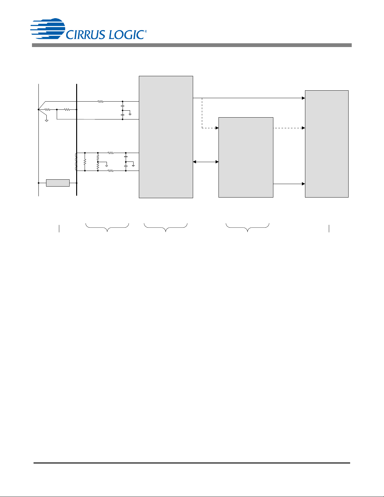
3.2 System Scale Example
CS 5480 / 84 / 90
(AF E)
LN
VIN-
VIN+
IIN+
IIN-
Application
Pro cessor
LOAD
CT
Pulse
Pulse
OR
Display
Power
19 .2 kW
240 V
RMS
,
80 A
RMS
176 m V
RMS
,
35 m V
RMS
19 .2 kW
240 V
RMS
,
80 A
RMS
Pavg: ±0.36
V
RMS
: 0.6
I
RMS
: 0.6
Hardware
Scale
AFE
Scale
MCU
Scale
19 .2 k W
240 V
RMS
,
80 A
RMS
Input Output
Seri al
Port
Figure 1 illustrates an example of the system scaling.
AN366
Figure 1. System Scaling
- Hardware Scale: The CS5480/ 84 /90 inputs are scaled using attenuation circuits that apply a maximum
input amplitude of 176mV
RMS
or 35mV
, which is dependent on an AFE gain setting of 10x gain or
RMS
50x gain, respectively.
- AFE Scale: The AFE registers record input levels that are displayed as a ratio of the most recent
measurement to the maximum RMS voltage and RMS current. The maximum RMS register value is
generated using a 0.6 ratio. The register value is read as a 24-bit hexadecimal number, which is
proportioned to represent a 0.6 V
the maximum power is P
- MCU Scale: The MCU is required to read all registers and interpret the 24-bit hexadecimal numbers
MAX
= V
full scale. At maximum voltage (0.6) and maximum current (0.6)
RMS
RMSMAX
× I
RMSMAX
= 0.6 × 0.6 = 0.36.
based on full-load conditions. Knowing the maximum hardware scaling and the most recent AFE
register values in relation to the full-scale input, the MCU routines are able to calculate the actual power
measurements.
AN366REV2 3
Page 4
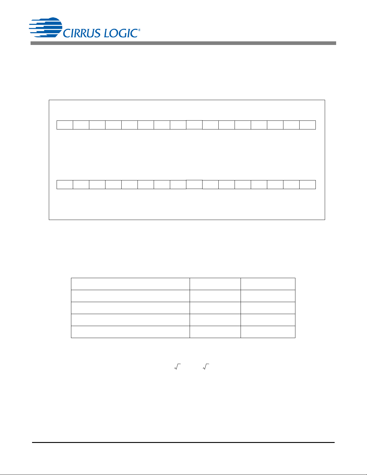
AN366
RMS 1 Current (I1
RMS
) – Page 16, Address 6
Default = 0x00 0000
I1
RMS
contains the root mean square (RMS) values of I1, calculated during each low-rate interval.
This is an unsigned value in the range of 0 value 1.0, with the binary point to the left of the MSB.
RMS Voltage 1 (V1
RMS
) – Page 16, Address 7
Default = 0x00 0000
V1
RMS
contains the root mean square (RMS) value of V1, calculated during each low-rate interval.
This is an unsigned value in the range of 0 value 1.0, with the binary point to the left of the MSB.
MSB LSB
2
-1
2
-2
2
-3
2
-4
2
-5
2
-6
2
-7
2
-8
.....
2
-182-192-202-212-222-232-24
MSB LSB
2
-1
2
-2
2
-3
2
-4
2
-5
2
-6
2
-7
2
-8
.....
2
-182-192-202-212-222-232-24
Figure 2. Example of I
RMS
and V
RMS
Registers
VALUE
Decimal
1
2
24
1–
------------------
hex2dec VALUE
Hexidecimal
=
[Eq: 1]
V
PEAK
V
RMS
2 0.6 2 0.85===
[Eq: 2]
3.3 AFE Scaling Range
The CS5484 full scale RMS register values are commonly reported as 0.6 when the inputs are at a maximum
level. The ratio of the AFE inputs to full scale defines the reference point for all other input levels. The 24-bit
I1
and V1
RMS
does not match the scaling for power (signed). Section 6.2 Main Calibration Flow Diagram Using the CDB5484
on page 29 describes the scaling ratio of the AFE inputs when maximum input levels are applied.
registers are defined in Figure 2. Note that the digital scaling for RMS current (positive only)
RMS
Use Equation 1 to convert the hexadecimal value to a decimal value:
Using Equation 1, the following key values are identified:
Key RMS Register Values Range (0 to 1) Decimal Value Register Value
Maximum RMS Register 1 0xFFFFFF
Maximum RMS Input 0.6 0x999999
Half RMS Input 0.36 0x5C28F6
No Load Input 0 0x000000
If a sine wave is applied to the voltage channel input at full scale, then the peak voltage can be determined using
Equation 2:
The V
The CS5480/84/ 90 provides a current channel scale register that allows a small load current during calibration.
By default, the range is 0.6 (full-scale current load), but this value can be adjusted according to the load current
available.
PEAK
register will have a maximum input margin of 15%, which prevents clipping.
4 AN366REV2
Page 5
AN366
ReportedCurrent
ACTUAL
Current
REGISTER
Current
FULLSCALE
0.6
-----------------------------------------------------------------------------------------------------------
0.25 50A
0.6
-----------------------------
20.8A===
[Eq: 3]
ReportedPower
ACTUAL
Power
REGISTER
Power
FULLSCALE
0.36
---------------------------------------------------------------------------------------------------
=
Power
REGISTER
Vch
FULLSCALE
Ich
FULLSCALE
0.36
---------------------------------------------------------------------------------------------------------------------------------------------
=
0.15 140 50
0.36
---------------------------------------------
2916.7W==
[Eq: 4]
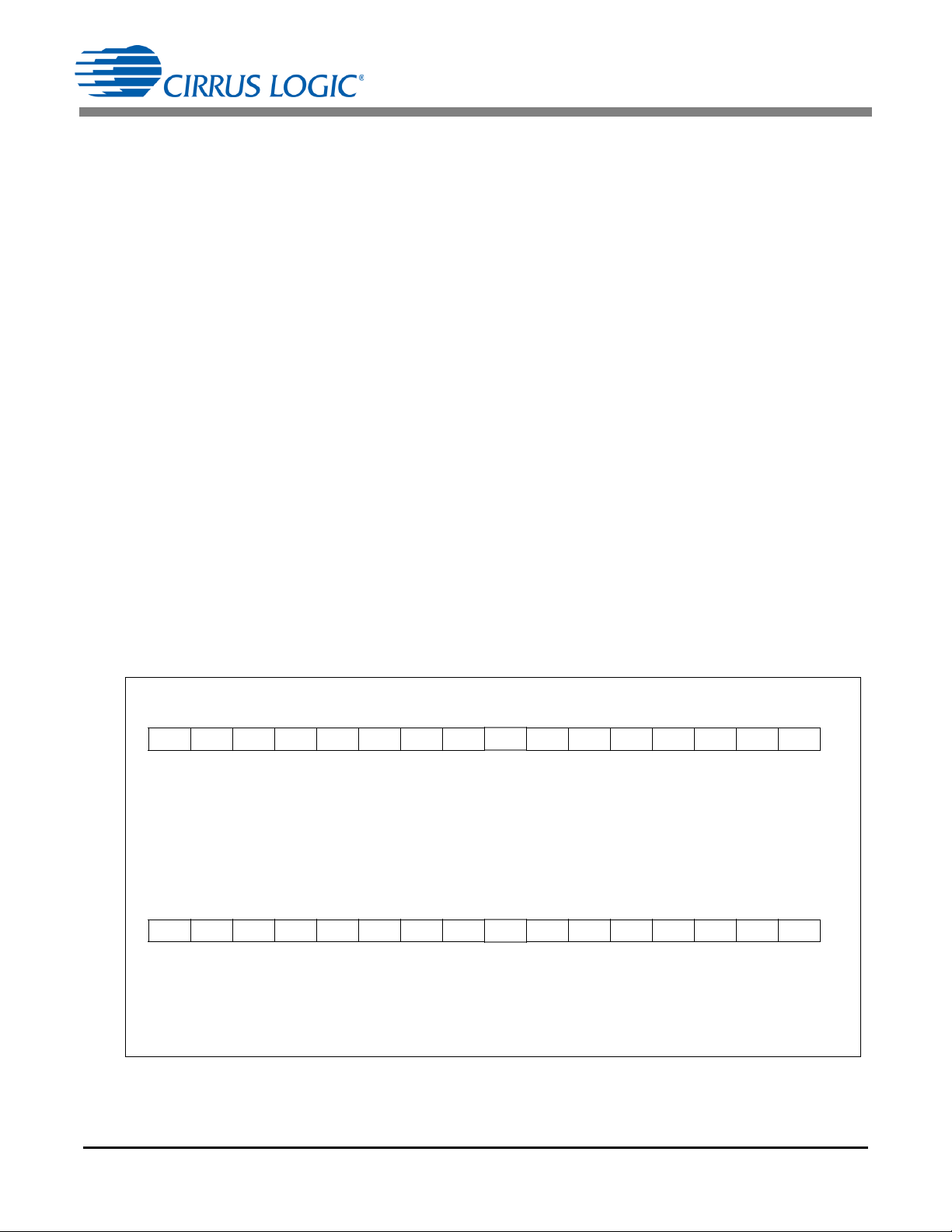
Active Power 1 (P1
AVG
) – Page 16, Address 5
Default = 0x00 0000
Instantaneous power is averaged over each low-rate interval (SampleCount samples) and then added
with power offset (P
OFF
) to compute active power (P
AVG
).
This is a two's complement value in the range of -1.0value1.0, with the binary point to the right of the
MSB.
Active Power 2 (P2
AVG
) – Page 16, Address 11
Default = 0x00 0000
Instantaneous power is averaged over each low-rate interval (SampleCount samples) to compute active
power (P2
AVG
).
This is a two's complement value in the range of -1.0value1.0, with the binary point to the right of the
MSB.
MSB LSB
-(20)2-12
-2
2
-3
2
-4
2
-5
2
-6
2
-7
.....
2
-172-182-192-202-212-222-23
MSB LSB
-(2
0
)2-12
-2
2
-3
2
-4
2
-5
2
-6
2
-7
.....
2
-172-182-192-202-212-222-23
Figure 3. Example of P1
AVG
and P2
AVG
Registers
3.4 Application Processor Scaling Example
The scaling example below demonstrates how to convert from the current register value to the reported current
using the full-scale value. The specified full-load (Current
(Current
REGISTER
) is 0.25 (0x40 0000), then the actual current value (ReportedCurrent
FULLSCALE
the application processor using Equation 3.
Use Equation 3 to convert the current register value to the real current:.
Scaling for power requires a change in the denominator to reflect a power scaling ratio of 0.36, which is equal
to the voltage (0.6) multiplied by current (0.6). The input full load (Ich
voltage (Vch
register (Power
FULLSCALE
REGISTER
) is 140V. If the present load is applied to the meter results in a power
) reading of 0.15 (0x13 3333), then the application processor needs to convert the
power register value to the real current value. Use Equation 4 to convert the power register value to real reported
power.
) is 50A. If the AFE current register value
) is calculated by
FULLSCALE
ACTUAL
) is 50A and the maximum
Cirrus Logic power meters are bidirectional, which allows power to be measured in both directions (consumed
or delivered). This reduces the digital scaling by one bit due to polarity, unlike the unsigned RMS current register.
The 24-bit P1
and P2
AVG
registers are defined in Figure 3.
AVG
AN366REV2 5
Page 6
AN366
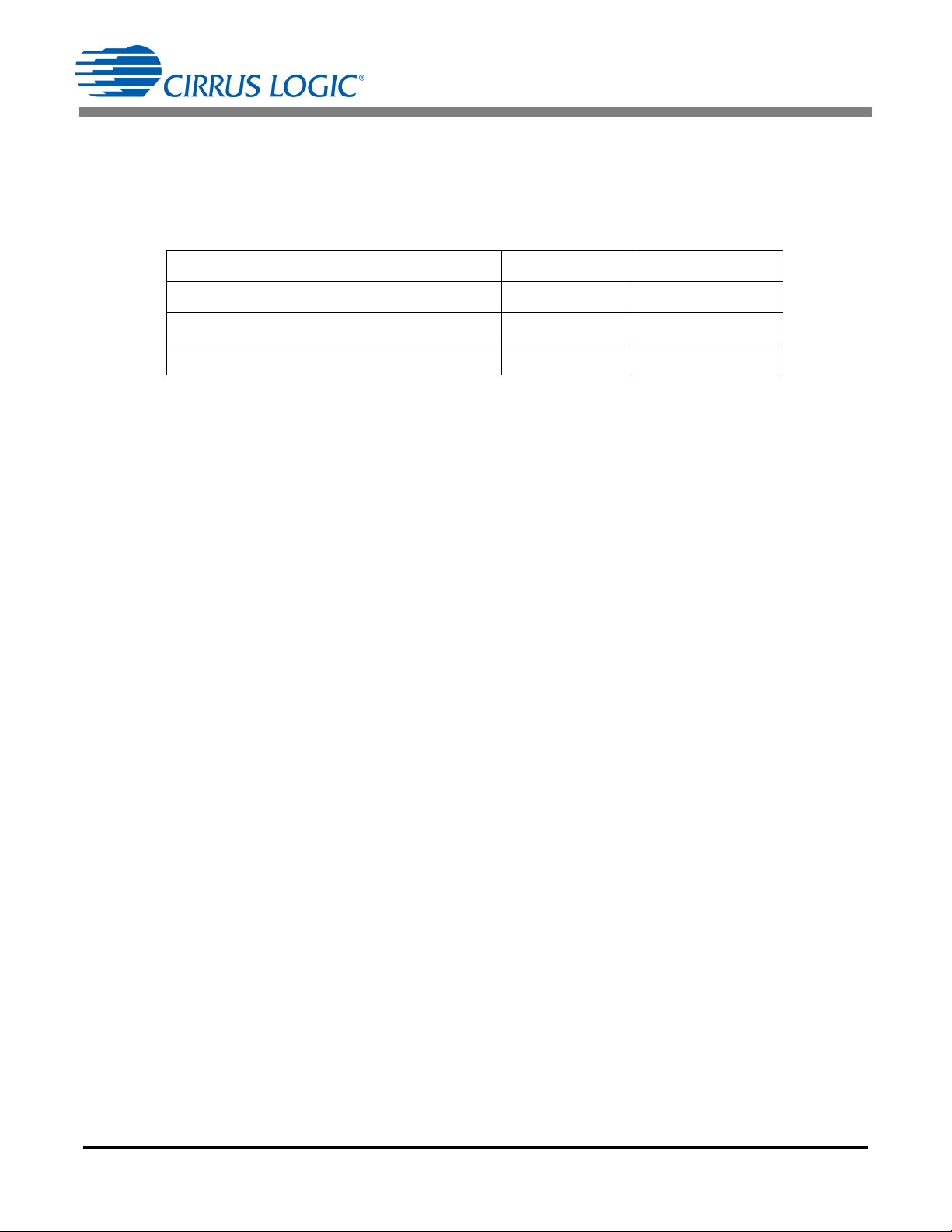
VALUE
Decimal
MSB–
1
2
23
1–
------------------
hex2dec VALUE
Hexidecimal
=
[Eq: 5]
Use Equation 5 to convert the hexadecimal value to a decimal ratio value:
Using Equation 5, the following table identifies the key values.
Key Power Register Values Range (-1 to 1) Decimal Value Register Value
Maximum Power Register 1 0x7FFFFF
Maximum Power Input 0.36 0x2E147B
No Load Input 0 0x000000
4 Types of Calibration and Compensations
Calibration is self-contained within the CS5480/ 84/ 90, and all calculations are performed by the device and
stored in internal registers. Compensations require that the MCU perform some of the calculations and then
store the results back into the CS5480/ 84 /90 registers. Since the CS5480/ 84 / 90 does not have non-volatile
memory (NVM), permanent storage of calibration and compensation must be placed in the MCU NVM and reloaded after any AFE reset condition.
In general, each calibration and compensation requires the following steps:
1. Configure the CS5480/84/ 90 initial conditions
2. Apply the analog input with stimulus from an accurate source
3. Enable the desired calibration
4. Execute calibration
5. Read the results
6. Calculate the new register values for compensations
7. Store the results in the AFE and NVM
It is common to perform calibration and compensation simultaneously. For example, since an AC gain calibration
and a phase compensation require a similar input signal to be applied to the current and voltage channels, calibration and compensation are performed simultaneously.
6 AN366REV2
Page 7
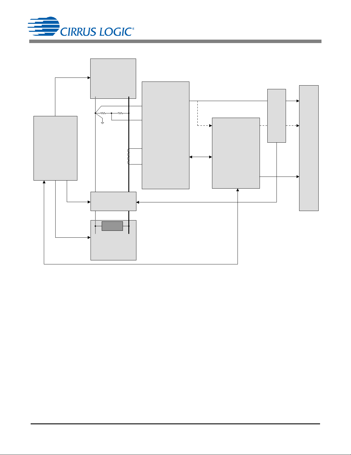
Figure 4 illustrates a typical hardware configuration for calibration and compensation:
AC
LOAD
AC
SOURCE
CS5480 /84 /90
(A FE)
LN
VIN -
VIN +
IIN +
IIN -
Application
Processor
LOAD
CT
Pulse
Pulse
OR
Display
Power
Seri al
Port
Reference
Meter
Optical
Sensor
Calibration
Controller
AN366
Automation can be established by a calibration controller that starts the calibration and/or the compensation,
performs the required calculations, and finally initiates the storage of results. A calibration controller will control
the AC source and load during calibration by adjusting the load for different AFE input conditions. The controller
will also monitor the precision reference meter to confirm that load adjustments have been successfully executed, and the optical accumulation results are accurate from the Cirrus AFE. Communication from the controller
to the Cirrus AFE is processed through the meter application processor to the calibration controller. Calculations
and NVM results stored within the application processor are initiated by the controller when the calibration is
completed.
AN366REV2 7
Figure 4. Calibration and Compensation Hardware Configuration
Page 8
AN366
V
RMS
*
, I
RMS
*
Registers
V*, I*, P*, Q
*
Registers
N
I
GAIN
*
, V
GAIN
*
Registers
*
Denotes readable/writable register
Ϯ Applies only to the curr ent path
N
N
-1
N
DC
RMS
-1
RMS
0.6(Scale
*
Ϯ
)
P
AVG
*
, Q
AVG
*
Registers
N
N
Modulator
I
DCOFF
*
, V
DCOFF
*
Registers
PC
Register
Sinc IIR
SYS
GAIN
Register
IN
P
OFF
*
, Q
OFF
*
Registers
I
ACOFF
*
Ϯ
Register
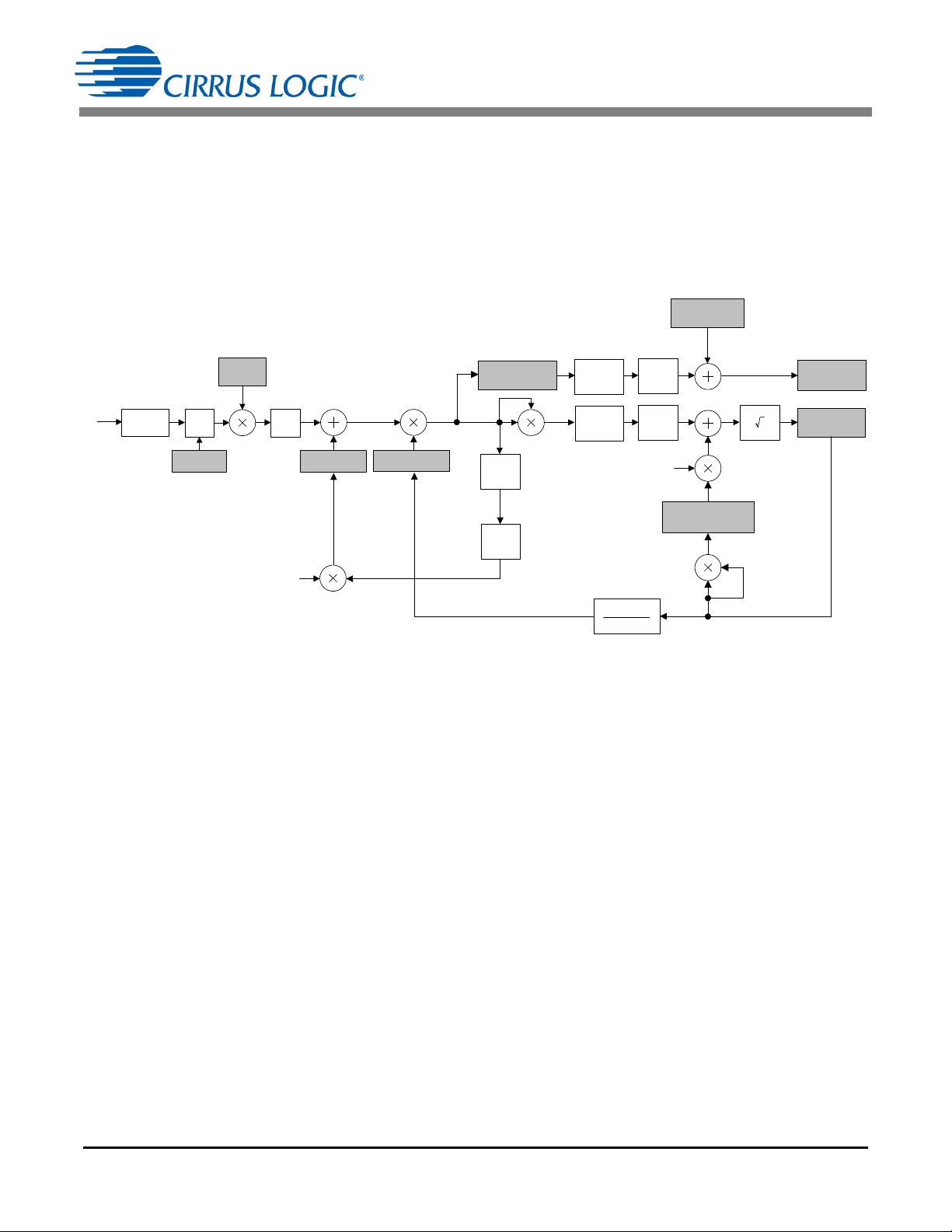
4.1 AFE Calibrations
The CS5480/84/90 AFE incorporates three calibrations: gain, AC offset, and DC offset. Gain calibration is always required. AC offset calibration is only required when I
offset calibration is made available but not recommended for AC power meters. Instead, high-pass filters are
used to remove DC offset. The high-pass filter included in the CS5480/ 84 /90 will remove any DC offset in real
time, and it is the best choice for AC power meters.
Figure 5 shows a flow diagram of the calibration process included in the Cirrus AFE. Refer to the CS5480/84/90
data sheet for detailed information.
needs to be accurate at low input levels. DC
RMS
Figure 5. Calibration Data Flow
4.1.1 DC Offset Calibration
DC offset calibration is designed to remove the DC component from the ADC output. DC offset calibration
is seldom used in AC power meters. The high-pass filter is the recommended choice and should be enabled
at the modulator output, as illustrated in Figure 5.
4.1.2 Gain Calibration
Gain calibration will adjust the input for hardware and sensor variations and customer-specific inputs. It is
recommended to use full-load conditions (full-scale voltage and current). (For non-full-load conditions, see
section 4.1.2.1 on page 8). When the full current load is not available, the CS5480/84/90 allows the scale
register to adjust for lower current loads to be provided. (See 3.3 on page 4 for adjusting the scale register.)
After gain calibration, full-scale input will yield:
- The Voltage RMS register, V
- The Current RMS register, I
- The Active Power register, P
- The Reactive Power register, Q
- The Apparent Power register, S, value: 0.6
4.1.2.1 When AC Source or AC Load Are Less Than Ideal
If the AC source or AC load are less than ideal, the meter can still be calibrated with an accurate reference
meter using the Non-full-scale Gain Calibration procedure on page 9. It is common to see an AC load set to
15A actually measure in the range of 14.55 A to 15.45A using a reference meter. When using the full-scale
, value: 0.6
RMS
, value: 0.6
RMS
, value: 0.6 0.6 = 0.36 at PF = 1
AVG
, value: 0.6 0.6 = 0.36 at PF = 0
AVG
0.6 = 0.36
current, it may be necessary to use the Non-full-scale Gain Calibration procedure on page 9 to account for
inaccurate resources.
8 AN366REV2
Page 9

AN366
V
GAIN pre
V
MAX
V
REF
---------------
2
22
=
[Eq: 6]
I
GAIN pre
I
MAX
I
REF
------------
2
22
=
[Eq: 7]
4.1.2.2 Non-full-scale Gain Calibration
When resources are limited, it may be necessary to provide non-full-scale amplitudes and perform built-in
calibration to provide the maximum voltage and current during calibration. To perform a non-full-scale calibration, the initial gain register conditions of the device must be identified before calibration. Usually, initial
gain register conditions are set to a default value of one, but this is not required. Instead, the initial gain register conditions are set to accommodate the non-full-scale input calibration. Before calibration is executed,
the gain register can be set using the following equations:
where:
V
GAIN(pre)
I
GAIN(pre)
V
MAX
I
MAX
V
REF
Value stored in voltage gain register (page 16, address 35) before calibration starts
Value stored in current gain register (page 16, address 33) before calibration starts
Maximum voltage of the meter defined by customer
Maximum current of the meter defined by customer
Voltage of the line just before calibration as measured with reference meter assumes
stable input
I
REF
Load current just before calibration as measured with reference meter assumes stable
input
Follow the steps below to perform a non-full-scale gain calibration:
1. Set the line voltage and load current V
2. Confirm that the reference meter shows V
3. Set V
GAIN(pre)
per Equation 6 and I
GAIN(pre)
and I
REF
REF
REF
and I
per Equation 7.
, respectively.
of the input.
REF
4. Send the calibration command.
5. After calibration, the meter is adjusted for a full-scale voltage of V
measuring the V
REF
and I
measurements.
REF
MAX
and I
and will currently be
MAX
Reference Limits
The calibration line voltage (V
) or load current (I
REF
) must not be set too low. It is recommended to keep
REF
the register values at a minimum of ½ of the maximum levels. Since the gain register can be set to a maximum value of 4, the input could be set to ¼ of the maximum levels. It is not recommended to set the input
to ¼ of the maximum levels due to variations in setup conditions. If the input is too low, the gain register will
set the default value of one after calibration.
AN366REV2 9
Page 10

AN366
I
SCALE
I
REF
I
MAX
------------
0.6 2
23
=
[Eq: 8]
Current Scale Register
To perform calibration with less than full scale load without using the above procedure, it is possible to set
the current channel's Scale register. The current channel calibration data path contains a Scale register
(page 18, address 63) that can be adjusted before calibration to accommodate the non-full-scale load.
where:
I
SCALE
I
MAX
I
REF
Value stored in the Scale register before calibration
Maximum current of the meter defined by the customer
Load current before calibration, as measured with a reference meter, assuming stable
input
Follow the steps below to set the current channel’s Scale register.
1. Set the load current, I
2. Confirm that the reference meter shows V
(assuming V
REF
is set to full scale).
REF
and I
REF
REF
of the input.
3. Set the Scale register per Equation 8.
4. Send the calibration command.
5. After calibration, the meter is adjusted for a full-scale voltage of V
measuring the V
REF
and I
measurements.
REF
MAX
and I
and will currently be
MAX
6. The Scale register is not in the normal data path but instead in the calibration path.
4.1.3 AC Offset Calibration
Following gain calibration, there may still be some AC offset remaining. AC offset calibration will allow for
the removal of the remaining offset. The AC offset effects are only applicable to the I
input. The AC offset calibration only needs to be performed when I
readings are required to span a large
RMS
registers at small
RMS
dynamic range with high accuracy.
4.2 Available Compensations
Three compensations are available in the CS5480/84/ 90: phase, no-load active power, and no-load reactive
power offset.
4.2.1 Phase Compensation
Phase compensation adjusts phase mismatches between the voltage and current channels. Setting the current to lag the voltage by 60º (the center of the COS range of 0º - 90º) allows the system to distinguish additional or less phase delay from the power factor (PF) directly. Follow the steps below to perform this
compensation:
1. Apply source at full scale with a 60º phase shift (PF = 0.5 lagging)
2. Start continuous convert
3. Read the PF register and calculate:
Phase error = ACOS(register PF)-60º
4. Calculate phase compensation (PC) register (MCLK=4.096MHz):
50Hz PC register = phase error/0.008789
60Hz PC register = phase error/0.010547
Phase error can be adjusted when it falls within ±8.99º at 50Hz or ±10.79º at 60Hz. Figure 6 shows the
phase offset error range. When phase error is below -4.5º at 50Hz or -5.4º at 60Hz and above 0 º, it is necessary to adjust both coarse compensation and fine compensation. The coarse and fine compensation settings for each region are shown in Figure 6.
10 AN366REV2
Page 11

AN366
0º
Before Calibration V is delayed from I
Delay added to I
8 .99 º @ 50 H z
10.79 º @ 60Hz
4.5º @ 50Hz
5.4º @ 60Hz
-4.5º @ 50Hz
-5.4º @ 60Hz
-8.99º @ 50 Hz
-10 .79 º @ 60Hz
Before Calibration I is delayed from V
Delay added to V
Set C PC C = 11 of 2OW R on V
+ FPC C prov i des adjus tm ent
Set C PC C = 10 of 1OW R on V
+ FPC C prov i des adjus tm ent
Clear CPCC = 00
+ FPC C prov i des adjus tm ent
Set CPCC = 01 of 1OWR on I
+ FPC C prov i des adjus tm ent
Figure 6. Phase Compensation and Phase Offset Error
4.2.2 No Load Power Compensation
There are two power compensations in the CS5480/ 84 / 90: active and reactive power offset. When no load
is applied, the average active power register, P
, and average reactive power register, Q
AVG
AVG
offsets. To remove any remaining active or reactive power, it is necessary to perform the following compensation:
- Apply full scale voltage source
- Apply no load to the current channel(s)
- Start continuous conversion
- Read P
- Write -P
and Q
AVG
and -Q
AVG
AVG
AVG
register
to P
OFF
and Q
, respectively
OFF
, may have
AN366REV2 11
Page 12

AN366
5 Calibration and Compensation Procedures
A CS5480/84/ 90 power meter normally has two modes of operation: calibration, which is executed only once at the
factory, and normal operation in the field.
Calibration will compensate for system-level errors and is only performed at the factory. Normal operation is a
continuous running mode (continuous conversion mode) or user-initiated, single execution mode (single conversion
mode). Most designs are continuously running and use the continuous conversion command. Normal operation is
resetting the device, loading calibration and configuration information from non-volatile memory, and executing
continuous conversion command. The MCU then needs to read various device registers to obtain the power, current,
and voltage. As these registers are updated, the MCU will need to post the information to the user interface. This is
accomplished by using DO pin interrupts or by periodically reading the status register. The default configuration of
the part sets most of the registers to a common configuration. When continuous conversion is performed, the device
will provide most register updates once per second (default at reset).
The normal field operation is simple and there is no need for extensive computation by the MCU. A simple, low cost
MCU may be used to assist the normal operation.
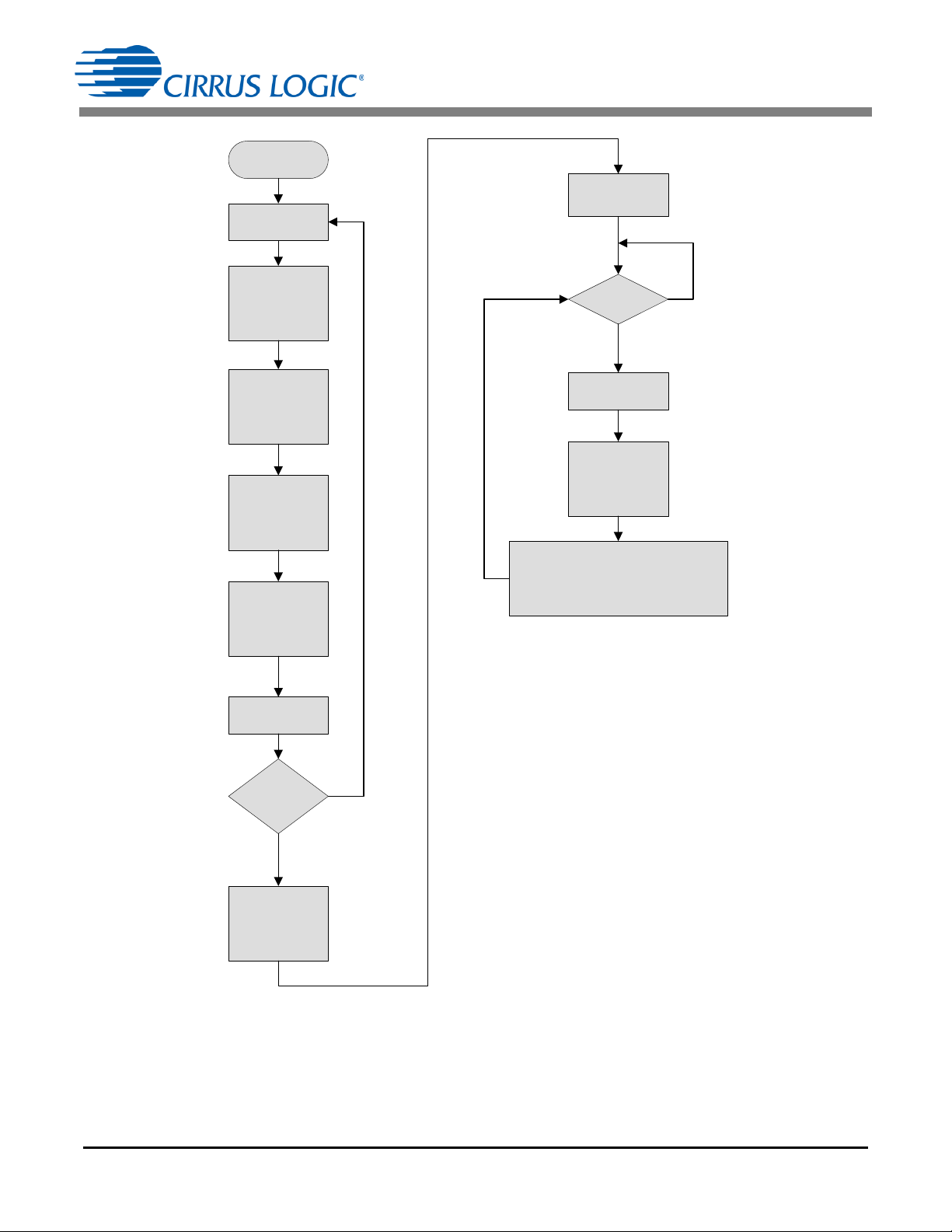
5.1 Normal Operation Procedure (Performed at Every Reset in the Field)
The following procedure outlines the steps required to put the meter in normal operation mode. Figure 7 shows
a simplified flow chart for the normal operation in the field.
1. Reset the CS5480/84 / 90.
2. Restore configuration and control registers.
3. Restore the V
GAIN
and I
registers from the non-volatile memory (NVM).
GAIN
4. If needed, restore the offset registers from NVM.
5. If needed, restore the phase compensation registers from the NVM.
6. If needed, restore the no load compensation to the P
OFF
and Q
OFF
7. Send the single conversion command to the CS5480/84/90.
8. Confirm that the register checksum is valid, or return to step 1.
9. Send the continuous conversion command to the CS5480/84/90.
10. Enable and clear DRDY.
11. Poll DRDY.
12. If DRDY is set, clear DRDY.
13. Read I
RMS
, V
RMS
, and P
. Scale the I
AVG
Amps = Full_Scale_Current
Volts = Full_Scale_Voltage
Watts = Full_Scale_Power
(I
(V
(P
RMS
RMS
AVG
RMS
/0.6)
/0.6)
/0.36)
, V
RMS
, and P
back into true value by:
AVG
14. Loop back to "Poll DRDY" step.
registers from the NVM.
12 AN366REV2
Page 13
START
CONTINUOUS
CONVERSION
0xD5
CLEAR
DRDY
READ IRMS,
VRMS, PAVG
DRDY
SET?
POWER UP
RESTORE
CONFIGURATION
and CONTROL
REGISTERS
From NVM
RESTORE
GAIN
REGISTERS
From NVM
RESTORE
OFFSET
REGISTERS
From NVM
RESTORE
POFF and QOFF
REGISTERS
CLEAR
DRDY
CALCULATE
VOLTS = FS_Voltage · (VRMS/0.6)
AMPS = FS_Current · (VRMS/0.6)
WATTS = FS_Scale _Pow er · (VRMS/0.36)
RESET
VALID
REGISTER
CHECKSUM
?
SINGLE
CONVERSION
YES
NO
YES
NO
Figure 7. Normal Field Flow
AN366
AN366REV2 13
Page 14

AN366
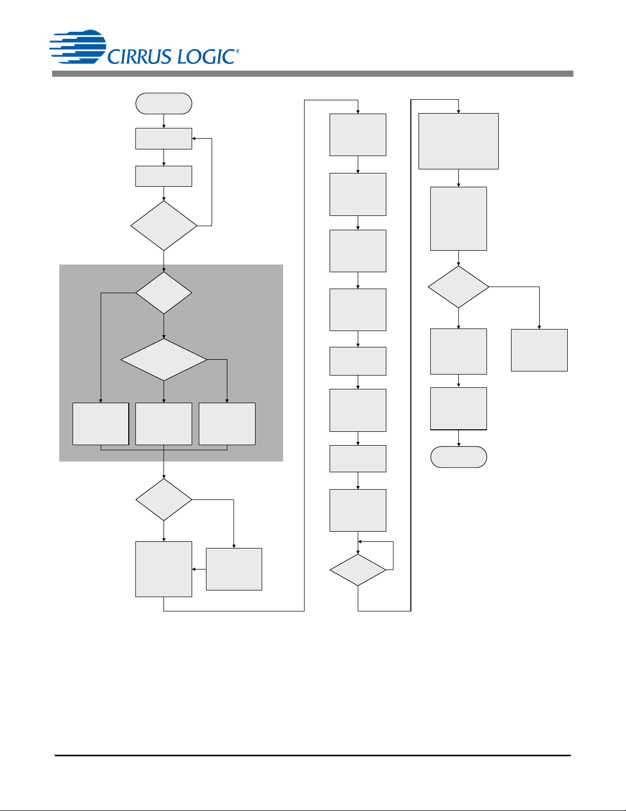
5.2 Full Calibration and Compensation Procedure (Performed Once at Factory)
The following procedure shows the steps required to perform calibration and compensation. A flow chart showing the full calibration procedure is shown in Figure 5.
1. Power up the CS5480/84/90 device.
2. Reset the CS5480/84 / 90 device.
3. Verify the register checksum to confirm the reset is successful.
4. Restore configuration and control registers.
5. Connect the reference line voltage and load current to the meter with a phase angle of 60º current lagging.
6. If the reference load current is not the full load, set the Scale register to a ratio of 0.6 2
current ÷ full scale current. See Non-full-scale Gain Calibration on page 9 if the reference line voltage is
lower than the maximum line voltage.
7. Perform continuous conversion (0xD5 command) for 2 seconds.
8. Stop the continuous conversion (0xD8 instruction).
9. Read I
attached by verifying if the I
RMS
, V
RMS
, P
, and PF, and confirm the reference voltage and current signals are correctly
AVG
RMS
, V
RMS
, P
, and PF are in a reasonable range.
AVG
10. Clear DRDY status bit.
11. Send AC gain calibration command (0xFE) to the CS5480/ 84 /90.
12. Wait for DRDY to be set.
23
reference load
13. If needed, perform phase compensation, AC offset calibration, and power offset correction.
14. Send continuous conversion (0xD8 command).
15. Verify measurement accuracy. Check the setup or fail the meter if the accuracy is not within specifications.
16. Read V
GAIN
, I
GAIN
, I
ACOFF
, P
OFF
, Q
, PC, and register checksum and save them into flash/eeprom.
OFF
17. Calibration completed.
14 AN366REV2
Page 15
RESET
(See Note 1)
ROGOWSKI
SENSOR?
ENABLE
HIGH PASS
FILTER
ENABLE
INTEGRATOR on
CURRENT &
HIGH PASS on
VOLTAGE
FULL LOAD
AVAILABLE ?
APPLY
REFERENCE
LINE VOLTAGE
AND LOAD
CURRENT
(Note 5)
SET SCALE
REGISTER
0.6 · LOAD ÷ FS
(Note 6)
READ
IRMS, VRMS,
PAVG, QAVG, PF
START
CONTINUOUS
CONVERT
0xD5
STOP
CONVERSIONS
0xD8
SEND AC GAIN
CALIBRAT ION
0xFE
ACCURACY
IN SPEC?
CHECK
SETUP or
FAIL
READ VGAIN,
IGAIN, IACOFF,
POFF, QOFF, PC,
RegChk
STORE
CALIBRAT ION
CONSTANTS &
REGISTER
CHECKSU M
POWER UP
CALIBRAT ION
COMPLETE
DC
MEASUREMENT?
PERFORM
DC
CALIBRAT ION
DRDY
SET?
SINGLE
CONVERSION
YES
NO
YES
NO
YES
NO
YES
NO
YES
NO
YES
NO
VALID RESET
CHECKSUM?
(Note 3)
CONFIRM
REFERENCE
SIGNALS ARE
APPLIED
CORRECTLY
Tsettle =
2000ms
(Note 2)
SampleCount (N) =
16,000
(Note 2)
START
CONTINUOUS
CONVERSION
AND VER IF Y
METER
ACCURACY
CLEAR
DRDY
PERFORM PHASE
COMPENSATI ON,
IACOFF CALIBRATION,
and POWER OFFSET
CORRECTION if
NECESSARY
Note 1: The default setting for all registers should be set before performing calibration. Resetting the device restores the default setting
for all registers.
Note 2: Larger numbers in the Tsettle and SampleCount registers will increase calibration precision.
Note 3: Other configurations and controls might be necessary.
Note 4: For an expanded view showing more information about the main calibration flow, see Main Calibration Flow Diagram Using the
CDB5484 on page 29.
Note 5: See Non-full-scale Gain Calibration on page 9.
Note 6: Scale register is only in calibration path and does not require resetting to 0.6 after the calibration.
Figure 8. Main Calibration Flow
AN366
AN366REV2 15
Page 16

RESOLUT ION
MULTIPLIER
0.008789 (50Hz)
(Note 1)
-8.9 9º <
PHASE OFF SET
< +8.99º (50Hz)
?
(Note 2)
PHASE OFF SET
NEGAT IVE
?
FINE
COMPENSAT ION
(FP CC) = -PHASE
OFFSET ÷
0.008789 (50Hz)
0 <
PHASE OFF SET
< 512 · 0.008789
(50Hz)
?
FINE
COMPENSAT ION
(FPCC) = PH ASE
OFFSET ÷
0.008789 (50Hz)
SET COAR SE
COMPENSAT ION
(CPCC = 01)
1 OWR on I
PHASE OFF SET =
PHASE OFF SET +
4.5º (50Hz)
SET COAR SE
COMPENSAT ION
(CPCC = 11)
2 OWR on V
PHASE OFF SET =
8.99º - PH ASE
OFFSET (50Hz)
FAIL
METER
PHASE COMPENSAT ION COMPLETE
(RETURN CPCC & FPCC to MAIN)
ACCUMULATE MULTIPLE
PF READ ING AND
CONFIRM PF = 0.5
SET COAR SE
COMPENSAT ION
(CPCC = 10)
1 OWR on V
PHASE OFF SET =
4.5º - PHASE
OFFSET
(50Hz)
±10.79º @ 60Hz
0.010547 @ 60H z
0 to 512 0.010547 @ 60 Hz-512 0.010547 to 0 @ 60 Hz
5.4º @ 60Hz 10.79º @ 60Hz5.4º @ 60Hz
0.010547 @ 60Hz
NO
YES
NOYES
NO
YES
NO
YES
-512 · 0.008789 <
PHASE OFF SET
< 0 (5 0Hz)
?
Note 4 Note 5
No co ar se
comp .
CPCC=00
APPLY
REFERENCE
LINE VOLT AGE
AND
60
O
LAGGING
LOAD CUR RENT
PF=0.5
START
CONTINUOUS
CONVERSI ON
0xD 5
FROM MAIN
FLOW
READ PF
CALCULATE
PHASE
OFFSET =
arccos(PF)-60º
STOP
CONVERSIONS
0xD 8
Tsettle =
2000 ms
(Note 1)
SampleCount
(N) = 16,000
(Note 1)
Figure 9. Phase Compensation Flow
Note 1:Larger numbers in the Tsettle and SampleCount registers will increase calibration precision.
Note 2: OWR= 4000, MCLK = 4.096 Mhz.
Note 3: For an expanded view showing more information about the phase compensation flow, see Phase Compensation Flow Diagram
on page 40.
Note 4: Before calibration: Angle < 60; Phase offset < 0; I leads V; PF is leading--for more positive, delay I.
Note 5: Before calibration: Angle < 60; Phase offset < 0; I lags V; PF is lagging--only coarse adjustment can delay V, therefore delay
V by 1 or 2 OWR and delay I by less than 1 or 2 OWR.
AN366
16 AN366REV2
Page 17

FROM MAIN
FLOW
CLEAR DRDY
SEND AC
OFFSET
CALIBRATI ON
0xF6
REMOVE LOAD
CURRENT
READ IRMS,
IACOFF
DRDY
SET?
CHECK
INPUT
OR
FAIL
RETURN
IACOFF
to
MAIN FLOW
IACOFF = 0
?
AC OFFSET
CALIBRATI ON
COMPLETE
Tsettle = 2000
SampleCount
N = 16000
NO
YES
YES
NO
Figure 10. AC Offset
Calibration Flow
Note: For an expanded view showing
more information about the AC offset
calibration flow, see AC Offset Calibration
Flow Diagram on page 44.
FROM MAIN
FLOW
CLEAR DRDY
SEND D C
OFFSET
CALIBRATION
0xE6
SHORT
VOLTAGE AND
CURRENT
INPUTS
READ IR MS,
VRMS, IDCOFF,
VDCOFF
DRDY
SET ?
CHECK
INPUT
OR
FAIL
RETURN
IDCOFF
VDCOFF
to
MAIN FLOW
IDCOFF = 0 ?
or
VDCOFF = 0 ?
DC OFF SET
CALIBRATION
COMPLETE
Tsettle = 2000
SampleCount
N = 16000
NO
YES
YES
NO
Figure 11. DC Offset
Calibration Flow
Note: For an expanded view showing
more information about the DC offset
calibration flow, see DC Offset
Calibration Flow Diagram on page 46.
FROM MAIN
FLOW
APPLY FU LL
SCALE VOLTAGE
AND ZERO LOAD
CURRENT
READ PAVG and
QAVG
DRDY
SET ?
RETURN
POFF
QOFF
to
MAIN FLOW
POWER OFFS ET
CALIBRATION
COMPLET E
Tsettle = 2000
SampleC ount
N = 16000
NEGATE
QAVG
& STORE IN
QOFF
NEGATE
PAVG
& STORE IN
POFF
START
CONTINUOUS
CONVERT
0xD5
NO
YES
CLEAR DRDY
Figure 12. No Load Offsets
Calibration Flow
Note: For more information, see No Load
Offset Compensation Flow Diagram on
page 47.
AN366
AN366REV2 17
Page 18

AN366
6 Full Calibration and Compensation Example Using the CDB5484 and MTE Meter Test
Equipment
The calibration and compensation flows have been implemented using the CDB5484U and a PC as the controller.
Using a MTE Meter Test Equipment AG PTS 400.3 Modular Portable Test System source and reference meter, the
results of this calibration can be shown. More information can be found by visiting the MTE Meter Test Equipment
website.
The CDB5484U connections are as follows:
1. The USB connects to the CDB5484U on the right. Using the standard CDB5484U GUI, commands and read
results from the Cirrus AFE can be sent.
2. The DUT supplies are connected to terminals J36 and J37. It is not recommended to use the USB supply to
power the Cirrus AFE during accuracy tests. Instead, use terminals J36 and J37.
3. Voltage is applied directly to the CDB5484U. Current inputs are looped through a terminal board and outputs are
sent to the CDB5484U.
4. The PC was connected to the RS232 connection on the MTE Meter Test Equipment power source and power
reference.
5. The pulse output is connected to an external counter or optically back to the MTE Meter Test Equipment power
reference.
6. The controller in this example is the CDB5484U and PC. While the CDB5484U is good for presentation, it is not
recommended to be used as a production solution.
18 AN366REV2
Page 19

AN366REV2 19
MTE Meter Test Equipment AG
PTS 400.3 Modular Portable Test System
Reference
Meter
Optical
Connection
AC
Source
Voltage Inputs
UART to PC Controller
Line Reference
Current Inputs
DUT Supply Rogowski Sensor USB to PC Controller
Pulse to Optical Counter
Figure 13. MTE Meter Test Equipment Calibration Hardware Setup
AN366
Page 20

POWER UP
From NVM
RESTOR E
FILTER
CONFIGURATION
RESET
21
AN366
6.1 Normal Operation Flow Diagram Using the CDB5484
The following flow diagram shows the implementation of normal flow executed in the field. The CDB5484U is
used to load calibration constants obtained during the factory calibration. Obviously, the GUI is not used during
actual execution, but it provides an excellent debugger for customer flow evaluation and modifications. The onetime factory calibration and compensation flows are discussed after the normal flow. The MTE Meter Test Equipment source is used to provide the source voltage and load current, but it is only required during this flow to
simulate different loading conditions. Each step of the flow shows the CDB5484U GUI screen capture of execution and reading results. The register writes and reads are all identified for easy comparison to the GUI screen.
POWER UP
Power up CDB5484U per data sheet using terminals J36 and J37.
RESET
SDI = 0xC1 Reset CS5484 software Reset
RESTORE FILTER CONFIGURATION
(See Figure 14.)
Config 2 Register
SDI = 0x90 0x40 0x0602AA Write Register Config2 to enable HPFs
SDO = 0xFF 0xFF 0xFFFFFF (Page 16, Register 0)
SDI = 0x90 0x00 0xFFFFFF Read Register Config2 to enable HPFs
SDO = 0xFF 0xFF 0x0602AA (Page 16, Register 0)
Figure 14. Setup Window
20 AN366REV2
Page 21

2
1
43
RESTOR E
CONFIGURATIONS
AN366
RESTORE REGISTERS
Various configurations include writes to registers (see Figure 14):
Config 0 Register
SDI = 0x80 0x40 0x400000 Write Register Config0
SDO = 0xFF 0xFF 0xFFFFFF (Page 0, Register 0)
SDI = 0x80 0x00 0xFFFFFF Read Register Config0
SDO = 0xFF 0xFF 0x400000 (Page 0, Register 0)
Config 1 Register
SDI = 0x80 0x41 0x10FEE0 Write Register Config1
SDO = 0xFF 0xFF 0xFFFFFF (Page 0, Register 1)
SDI = 0x80 0x01 0xFFFFFF Read Register Config1
SDO = 0xFF 0xFF 0x10FEE0 (Page 0, Register 1)
Pulse Control Register
SDI = 0x80 0x49 0x000000 Write Register Pulse Control
SDO = 0xFF 0xFF 0xFFFFFF (Page 0, Register 9)
SDI = 0x80 0x09 0xFFFFFF Read Register Pulse Control
SDO = 0xFF 0xFF 0x000000 (Page 0, Register 9)
Phase Comp Register
SDI = 0x80 0x45 0x007C40 Write Register Phase Compensation
SDO = 0xFF 0xFF 0xFFFFFF (Page 0, Register 5)
SDI = 0x80 0x05 0xFFFFFF Read Register Phase Compensation
SDO = 0xFF 0xFF 0x007C40 (Page 0, Register 5)
Pulse Width Register
SDI = 0x80 0x48 0x0613F0 Write Register Pulse Width
SDO = 0xFF 0xFF 0xFFFFFF (Page 0, Register 8)
SDI = 0x80 0x08 0xFFFFFF Read Register Pulse Width
SDO = 0xFF 0xFF 0x0613F0 (Page 0, Register 8)
Pulse Rate Register
SDI = 0x92 0x5C 0x800000 Write Register Pulse Rate
SDO = 0xFF 0xFF 0xFFFFFF (Page 18, Register 28)
SDI = 0x92 0x1C 0xFFFFFF Read Register Pulse Rate
SDO = 0xFF 0xFF 0x800000 (Page 18, Register 28)
Sample Count Register
SDI = 0x90 0x73 0x000FA0 Write Register Sample Count
SDO = 0xFF 0xFF 0xFFFFFF (Page 16, Register 51)
SDI = 0x90 0x33 0xFFFFFF Read Register Sample Count
SDO = 0xFF 0xFF 0x000FA0 (Page 16, Register 51)
Settle Time
SDI = 0x90 0x79 0x800000 Write Register T Settle
SDO = 0xFF 0xFF 0xFFFFFF (Page 16, Register 57)
SDI = 0x90 0x39 0xFFFFFF Read Register T Settle
SDO = 0xFF 0xFF 0x800000 (Page 16, Register 57)
AN366REV2 21
Page 22

AN366
From NVM
RESTORE
GAIN
CONFIGURATION
6
5
43
RESTORE GAIN CONFIGURATION
(See Figure 15.)
Gain Channel 1, Volt.
SDI = 0x90 0x63 0x401BE3 Write Register V1 Gain
SDO = 0xFF 0xFF 0xFFFFFF (Page 16, Register 35)
SDI = 0x90 0x23 0xFFFFFF Read Register V1 Gain
SDO = 0xFF 0xFF 0x401BE3 (Page 16, Register 35)
Gain Channel 1, Curr.
SDI = 0x90 0x61 0x3C4420 Write Register I1 Gain
SDO = 0xFF 0xFF 0xFFFFFF (Page 16, Register 33)
SDI = 0x90 0x21 0xFFFFFF Read Register I1 Gain
SDO = 0xFF 0xFF 0x3C4420 (Page 16, Register 33)
Gain Channel 2, Volt.
SDI = 0x90 0x6A 0x4037B6 Write Register V2 Gain
SDO= 0xFF 0xFF 0xFFFFFF (Page 16, Register 42)
SDI= 0x90 0x2A 0xFFFFFF Read Register V2 Gain
SDO= 0xFF 0xFF 0x4037B6 (Page 16, Register 42)
Gain Channel 2, Curr.
SDI = 0x90 0x68 0x3C465F Write Register I2 Gain
SDO = 0xFF 0xFF 0xFFFFFF (Page 16, Register 40)
SDI = 0x90 0x28 0xFFFFFF Read Register I2 Gain
SDO= 0xFF 0xFF 0x3C465F (Page 16, Register 40)
Figure 15. Calibration Window
22 AN366REV2
Page 23

From NVM
RESTORE
OFFSET
CONFIGURATION
87
6
5
AN366
RESTORE OFFSET CONFIGURATION
(See Figure 15.)
DC Offset Channel 1, Volt.
SDI = 0x90 0x62 0x000000 Write Register V1 DC Offset
SDO = 0xFF 0xFF 0xFFFFFF (Page 16, Register 34)
SDI = 0x90 0x22 0xFFFFFF Read Register V1 DC Offset
SDO = 0xFF 0xFF 0x000000 (Page 16, Register 34)
DC Offset Channel 1, Curr.
SDI = 0x90 0x60 0x000000 Write Register I1 DC Offset
SDO = 0xFF 0xFF 0xFFFFFF (Page 16, Register 32)
SDI = 0x90 0x20 0xFFFFFF Read Register I1 DC Offset
SDO = 0xFF 0xFF 0x000000 (Page 16, Register 32)
DC Offset Channel 2, Volt.
SDI = 0x90 0x69 0x000000 Write Register V2 DC Offset
SDO = 0xFF 0xFF 0xFFFFFF (Page 16, Register 41)
SDI = 0x90 0x29 0xFFFFFF Read Register V2 DC Offset
SDO = 0xFF 0xFF 0x000000 (Page 16, Register 41)
DC Offset Channel 2, Curr.
SDI = 0x90 0x67 0x000000 Write Register I2 DC Offset
SDO = 0xFF 0xFF 0xFFFFFF (Page 16, Register 39)
SDI = 0x90 0x27 0xFFFFFF Read Register I2 DC Offset
SDO = 0xFF 0xFF 0x000000 (Page 16, Register 39)
AC Offset Channel 1, Curr.
SDI = 0x90 0x65 0x050704 Write Register I1 AC Offset
SDO = 0xFF 0xFF 0xFFFFFF (Page 16, Register 37)
SDI = 0x90 0x25 0xFFFFFF Read Register I1 AC Offset
SDO = 0xFF 0xFF 0x050704 (Page 16, Register 37)
AC Offset Channel 2, Curr.
SDI = 0x90 0x6C 0x049959 Write Register I2 AC Offset
SDO = 0xFF 0xFF 0xFFFFFF (Page 16, Register 44)
SDI = 0x90 0x2C 0xFFFFFF Read Register I2 AC Offset
SDO = 0xFF 0xFF 0x049959 (Page 16, Register 44)
AN366REV2 23
Page 24

From NVM
RESTORE
NO LOAD
CONFIGURATION
10
9
87
SINGLE
CONVERSION
AN366
RESTORE NO LOAD CONFIGURATION
(See Figure 15.)
P1 Offset
SDI = 0x90 0x64 0x000003 Write Register P1 Active Power Offset
SDO = 0xFF 0xFF 0xFFFFFF (Page 16, Register 36)
SDI = 0x90 0x24 0xFFFFFF Read Register P1 Active Power Offset
SDO = 0xFF 0xFF 0x000003 (Page 16, Register 36)
Q1 Offset
SDI = 0x90 0x66 0x000002 Write Register Q1 Reactive Power Offset
SDO = 0xFF 0xFF 0xFFFFFF (Page 16, Register 38)
SDI = 0x90 0x26 0xFFFFFF Read Register Q1 Reactive Power Offset
SDO = 0xFF 0xFF 0x000002 (Page 16, Register 38)
P2 Offset
SDI = 0x90 0x6B 0x000001 Write Register P2 Active Power Offset
SDO = 0xFF 0xFF 0xFFFFFF (Page 16, Register 43)
SDI = 0x90 0x2B 0xFFFFFF Read Register P2 Active Power Offset
SDO = 0xFF 0xFF 0x000001 (Page 16, Register 43)
Q2 Offset
SDI = 0x90 0x6D 0x000002 Write Register Q2 Reactive Power Offset
SDO = 0xFF 0xFF 0xFFFFFF (Page 16, Register 45)
SDI = 0x90 0x2D 0xFFFFFF Read Register Q2 Reactive Power Offset
SDO = 0xFF 0xFF 0x000002 (Page 16, Register 45)
SINGLE CONVERSION
(See Figure 16.)
Figure 16. Conversion Window
24 AN366REV2
Page 25

9 10
11
NO
YES
VALID
REGISTER
CHECKSUM
?
AN366
VALID REGISTER CHECKSUM?
Read register checksum and compare to stored value in NVM (see Figure 17).
SDI = 0x90 0x01 0xFFFFFF Read Register Checksum
SDO = 0xFF 0xFF 0x5C0ED4 (Page 16, Register 1)
Figure 17. Setup Window
AN366REV2 25
Page 26
AN366
WAIT 2 SEC
Tsettle = 2000ms
START
CONTINUOUS
CONVERSI ON
0xD5
11
12
CLEAR DRDY
DRDY
SET?
NO
YES
13
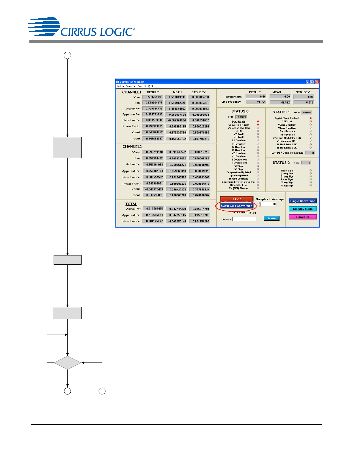
START CONTINUOUS CONVERSION
(See Figure 18.)
SDI = 0xD5 Send Continuous Conversion Command
Figure 18. Conversion Window
WAIT FOR TSETTLE TIME
Wait for Tsettle time.
CLEAR DRDY in INTERRUPT STATUS
SDI = 0x80 0x57 0x800000 Write DRDY Interrupt in Status 0
SDO = 0xFF 0xFF 0xFFFFFF (Page 0, Register 23)
DRDY SET?
SDI = 0x80 0x18 0xFFFFFF Read Status 1 for DRDY Interrupt (Not Set).
SDO = 0xFF 0xFF 0x4XXXXX (Page 0, Register 24)
SDI = 0x80 0x18 0xFFFFFF Read Status 1 for DRDY Interrupt (Set).
SDO = 0xFF 0xFF 0xCXXXXX (Page 0, Register 24)
26 AN366REV2
Page 27

CLEAR DRDY in INTERRUPT STATUS
READ IR MS,
VRMS, PAVG
CLEAR
DRDY
14
12 13
15
SDI = 0x80 0x57 0x800000 Write DRDY Interrupt in Status 0
SDO = 0xFF 0xFF 0xFFFFFF (Page 0, Register 23)
AN366
READ IRMS, VRMS PAVG
(See Figure 19.)
Channel 1
SPI = 0x06 0xFFFFFF Read I1RMS
SPO = 0xFF 0x999357 (Page 16 Register 6)
SPI = 0x07 0xFFFFFF Read V1RMS
SPO = 0xFF 0x998956 (Page 16 Register 7)
SPI = 0x05 0xFFFFFF Read P1AVG
SPO = 0xFF 0x2E0DC1 (Page 16 Register 5)
SPI = 0x14 0xFFFFFF Read S1
SPO = 0xFF 0x2E0DB8 (Page 16 Register 20)
SPI = 0x0E 0xFFFFFF Read Q1AVG
SPO = 0xFF 0x001226 (Page 16 Register 14)
SPI = 0x15 0xFFFFFF Read PF1
SPO = 0xFF 0x7FFFFF (Page 16 Register 21)
SPI = 0x13 0xFFFFFF Read V1PEAK
SPO = 0xFF 0x6C9FCE (Page 16 Register 19)
SPI = 0x12 0xFFFFFF Read I1PEAK
SPO = 0xFF 0x6CA12A (Page 16 Register 18)
Channel 2
SPI = 0x0C 0xFFFFFF Read I2RMS
SPO = 0xFF 0x9993FE (Page 16 Register 12)
SPI = 0x0D 0xFFFFFF Read V2RMS
SPO = 0xFF 0x9989D4 (Page 16 Register 13)
SPI = 0x0B 0xFFFFFF Read P2AVG
SPO = 0xFF 0x2E0E17 (Page 16 Register 11)
SPI = 0x18 0xFFFFFF Read S2
SPO = 0xFF 0x2E0E10 (Page 16 Register 24)
SPI = 0x10 0xFFFFFF Read Q2AVG
SPO = 0xFF 0x00122C (Page 16 Register 16)
SPI = 0x19 0xFFFFFF Read PF2
SPO = 0xFF 0x7FFFFF (Page 16 Register 25)
SPI = 0x17 0xFFFFFF Read V2PEAK
SPO = 0xFF 0x935EC4 (Page 16 Register 23)
SPI = 0x16 0xFFFFFF Read I2PEAK
SPO = 0xFF 0x6CA002 (Page 16 Register 22)
Total
SPI = 0x1D 0xFFFFFF Read PSUM
SPO = 0xFF 0x5C1BD6 (Page 16 Register 29)
SPI = 0x1E 0xFFFFFF Read SSUM
SPO = 0xFF 0x5C1BBE (Page 16 Register 30)
SPI = 0x1F 0xFFFFFF Read QSUM
SPO = 0xFF 0x0024DE (Page 16 Register 31)
SPI = 0x1B 0xFFFFFF Read T
SPO = 0xFF 0x000000 (Page 16 Register 27)
SPI = 0x31 0xFFFFFF Read Epsilon
SPO = 0xFF 0x019943 (Page 16 Register 49)
AN366REV2 27
Page 28

AN366
1514
CALCULATE
VOLTS = FS_Voltage
(VRMS/0.6)
AMPS = FS_Current
(VRMS/0.6)
WATTS = FS_Scale _Power
(VRMS/0.36)
Figure 19. Conversion Window
CALCULATE VOLTS, AMPS, AND WATTS
Channel 1
AMPS1 = HEX2DEC(I1RMS) / 0xFFFFFF / 0.6
VOLTS1 = HEX2DEC(V1RMS) / 0xFFFFFF / 0.6 FS_Voltage
If (P1AVG ≤ 0x7FFFFF) Then
WATTS1 = HEX2DEC(P1AVG) / 0x7FFFFF / 0.36 FS_Power
Else
WATTS1 = (HEX2DEC(P1AVG) - 0xFFFFFF) / 0x7FFFFF / 0.36
Channel 2
AMPS2 = HEX2DEC(I2RMS)/0xFFFFFF / 0.6
VOLTS2 = HEX2DEC(V2RMS) / 0xFFFFFF / 0.6
If (P2AVG ≤ 0x7FFFFF) Then
WATTS2 = HEX2DEC(P2AVG) / 0x7FFFFF / 0.36
Else
WATTS2 = (HEX2DEC(P2AVG) - 0xFFFFFF) / 0x7FFFFF / 0.36
FS_Current
FS_Power
FS_Current
FS_Voltage
FS_Power
FS_Power
28 AN366REV2
Page 29

RESET
POWER UP
1 2
AN366
6.2 Main Calibration Flow Diagram Using the CDB5484
The following flow diagram shows the implemented of gain calibration using the CDB5484U and a PC as the
controller. The MTE source is used to provide the source voltage and load current. Each step of the flow shows
the CDB5484 GUI screen capture of execution and reading results. The register writes and reads are all identified for easy compares to the GUI screen. The GUI is not promoted for production level calibration but does provide an excellent debugger for customer flow evaluation.
POWER UP
Power up CDB5484U per data sheet using terminals J36 and J37.
RESET
(See Figure 20.)
SDI = 0xC1 Reset CS5484 software Reset.
Figure 20. Setup Window
AN366REV2 29
Page 30

SINGLE
CONVERSION
1 2
3
YES
NO
VALID
RESET
REGISTER
CHECKS UM
?
AN366
SINGLE CONVERSION
The register checksum is computed each time a conversion is completed (Single or Continuous).
(See Figure 21.)
SDI = 0xD4 Send Single Conversion Command
Figure 21. Conversion Window
VALID REGISTER CHECKSUM TEST
PC/Controller tests if valid checksum is received (see Figure 22).
SDI = 0x90 0x01 0xFFFFFF Read Register Checksum
SDO = 0xFF 0xFF 0x46ECA1
Figure 22. Setup Window
30 AN366REV2
Page 31

AN366
4
3
ENABLE
HIGH PASS
FILTER
ENABLE HIGH PASS ON VOLTAGE AND CURRENT
(See Figure 23.)
SDI = 0x90 0x40 0x0602AA Write Register Config2 to enable HPFs
SDO = 0xFF 0xFF 0xFFFFFF
SDI = 0x90 0x00 0xFFFFFF Read Register Config2 to enable HPFs
SDO = 0xFF 0xFF 0x0602AA
Figure 23. Setup Window
AN366REV2 31
Page 32

AN366
APPLY FU LL-
SCALE ( FS)
VOLTAGE
TO SOURCE
PF=1
FULL LOAD
AVAILABLE ?
APPLY
LOAD
SET SCALE
REGISTER
0.6
LOAD ÷ FS
4
5
YES
NO
PERFOR M
PHASE
COMPENSAT ION
6
APPLY FULL-SCALE VOLTAGE TO SOURCE
(See Figure 24.)
Figure 24. Meter Test Equipment
See Non-full-scale Gain Calibration on page 9.
FULL LOAD AVAILABLE
PC/Controller knows if full load or partial load is available (see Figure 25 for partial load).
SDI = 0x92 0x7F 0x200000 Write Scale 0.25
SDO = 0xFF 0xFF 0xFFFFFF
SDI = 0x92 0x3F 0xFFFFFF Read Scale 0.25
SDO = 0xFF 0xFF 0x200000
Figure 25. Calibration Window
32 AN366REV2
Page 33

SET TSETTLE
Tsettle =
2000 ms
SampleCount
(N) = 16,000
5
7
8
6
(See Figure 26.)
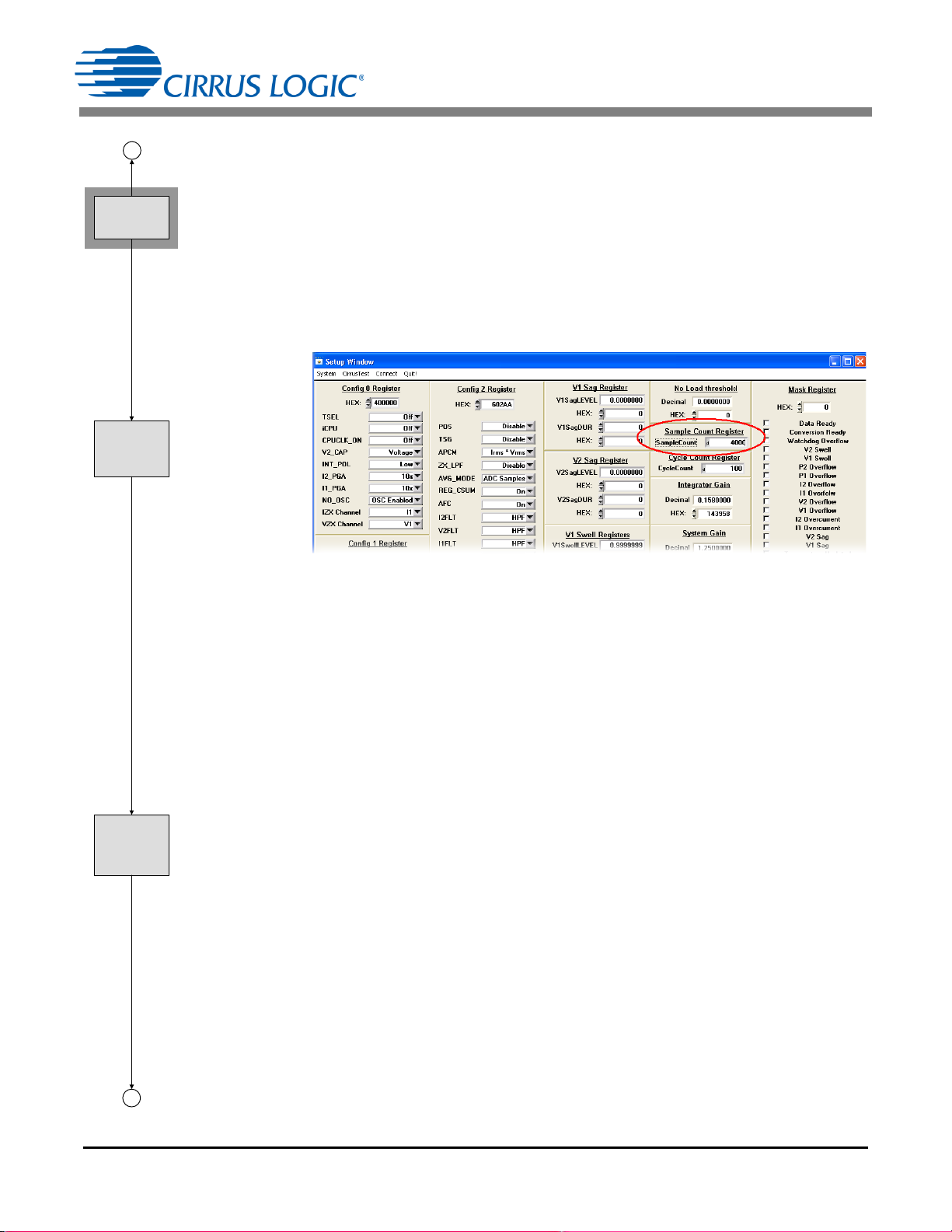
SDI = 0x90 0x79 0x001F40 Write TSETTLE = 2000ms
SDO = 0xFF 0xFF 0xFFFFFF (Page 16, Register 57)
SDI = 0x90 0x39 0xFFFFFF Read TSETTLE = 2000ms
SDO = 0xFF 0xFF 0x001F40 (Page 16, Register 57)
AN366
Figure 26. Setup Window
SET SAMPLE COUNT
(See Figure 27.)
SDI = 0x90 0x73 0x003E80 Write Sample Count = 16,000
SDO = 0xFF 0xFF 0xFFFFFF (Page 16, Register 51)
SDI = 0x90 0x33 0xFFFFFF Read Sample Count = 16,000
SDO = 0xFF 0xFF 0x003E80 (Page 16, Register 51)
Figure 27. Setup Window
AN366REV2 33
Page 34

START CONTINUOUS CONVERSION
READ
IRMS, VRMS,
PAVG, QAVG, PF
START
CONTINUOUS
CONVERT
0xD5
7
9 10
8
(See Figure 28.)
SDI = 0xD5 Write Continuous Conversion
SDO = 0xFF
AN366
Figure 28. Conversion Window
START CONTINUOUS CONVERSION
(See Figure 28.)
Channels 1 and 2, Current
SDI = 0x90 0x06 0xFFFFFF Read I1RMS (page 16, register 6)
SDO = 0xFF 0xFF 0x9AC11C (0.604509151)
SDI = 0x90 0x0C 0xFFFFFF Read I2RMS (page 16, register 12)
SDO = 0xFF 0xFF 0x9ABB62 (0.604421771)
Channels 1 and 2, Voltage
SDI = 0x90 0x07 0xFFFFFF Read V1RMS (page 16, register 7)
SDO = 0xFF 0xFF 0xA3A8BE (0.63929359)
SDI = 0x90 0x0D 0xFFFFFF Read V2RMS (page 16, register 13)
SDO = 0xFF 0xFF 0xA396E2 (0.639021077)
Channels 1 and 2, Active Power
SDI = 0x90 0x05 0xFFFFFF Read P1AVG (page 16, register 5)
SDO = 0xFF 0xFF 0x3177E9 (0.386471914)
SDI = 0x90 0x0B 0xFFFFFF Read P2AVG (page 16, register 11)
SDO = 0xFF 0xFF 0x3170AF (0.3862514)
Channels 1 and 2, Reactive Power
SDI = 0x90 0x0E 0xFFFFFF Read Q1AVG (page 16, register 14)
SDO = 0xFF 0xFF 0x000A92 (0.0003226)
SDI = 0x90 0x10 0xFFFFFF Read Q2AVG (page 16, register 16)
SDO = 0xFF 0xFF 0x000C84 (0.0003819)
Channels 1 and 2, Power Factor
SDI = 0x90 0x15 0xFFFFFF Read PF1 (page 16, register 21)
SDO = 0xFF 0xFF 0x7FFFFF (1)
SDI = 0x90 0x19 0xFFFFFF Read PF2 (page 16, register 25)
SDO = 0xFF 0xFF 0x7FFFFF (1)
Total
SDI = 0x90 0x1D 0xFFFFFF Read PSUM (page 16, register 29)
SDO = 0xFF 0xFF 0x000000 (0)
SDI = 0x90 0x1E 0xFFFFFF Read QSUM (page 16, register 30)
SDO = 0xFF 0xFF 0x000000 (0)
SDI = 0x90 0x1F 0xFFFFFF Read SSUM (page 16, register 31)
SDO = 0xFF 0xFF 0x000000 (0)
34 AN366REV2
Page 35

IS PF=1?
STOP
CONVERSIONS
0xD8
IS PF = 1 ?
CLEAR DRDY
SEND AC GAI N
CALIBRATI ON
0xFE
9
11
YES
10
NO
PC/Controller tests if PF returned is 1.
AN366
STOP CONVERSIONS
(See Figure 29.)
SDI = 0xD8 Write Halt Conversion
SDO = 0xFF
Figure 29. Conversion Window
CLEAR DRDY in INTERRUPT STATUS
SDI = 0x80 0x57 0xFFFFFF Write INT STATUS DRDY (page 0, register 23)
SDO = 0xFF 0xFF 0x800000 (Set DRDY INT)
SEND AC GAIN CALIBRATION
(See Figure 30.)
SDI = 0xFE Write Gain Calibration – All Channels
SDO = 0xFF
Figure 30. Calibration Window
AN366REV2 35
Page 36

READ IRMS,
VRMS, PAVG,
PSUM, QSUM,
SSUM
DRDY
SET ?
VRMS = 0.6 ?
IRMS = SCALE(0.6)?
PAVG = 0.36 ?
CHECK
SETUP o r
FAIL
SCALE = 0.25, T herefore
IRMS = 0.25 after calibration
YES
NO
YES
NO
12
YES
NO
11
PERFORM
NO LOAD
COMPENSATION
& READ PAVG
AN366
CHECK STATUS OF DRDY
SDI = 0x80 0x17 0xFFFFFF Read INT STATUS DRDY (page 0, register 23)
SDO = 0xFF 0xFF 0x4XXXXX (DRDY not Set)
SDI = 0x80 0x17 0xFFFFFF Read INT STATUS DRDY (page 0, register 23)
SDO = 0xFF 0xFF 0xCXXXXX (DRDY Set)
READ POWER REGISTERS
(See Figure 31.)
SDI = 0x90 0x06 0xFFFFFF Read I1RMS (page 16, register 6)
SDO = 0xFF 0xFF 0x40081D (0.2501238)
SDI = 0x90 0x0C 0xFFFFFF Read I2RMS (page 16, register 12)
SDO = 0xFF 0xFF 0x40086D (0.2501286)
SDI = 0x90 0x07 0xFFFFFF Read V1RMS (page 16, register 7)
SDO = 0xFF 0xFF 0x99ACE6 (0.6002945)
SDI = 0x90 0x0D 0xFFFFFF Read V2RMS (page 16, register 13)
SDO = 0xFF 0xFF 0x99ADA6 (0.600306)
SDI = 0x90 0x05 0xFFFFFF Read P1AVG (page 16, register 5)
SDO = 0xFF 0xFF 0x133936 (0.1501835)
SDI = 0x90 0x0B 0xFFFFFF Read P2AVG (page 16, register 11)
SDO = 0xFF 0xFF 0x133966 (0.1501892)
SDI = 0x90 0x1D 0xFFFFFF Read PSUM (page 16, register 29)
SDO = 0xFF 0xFF 0x266DFD (0.3002316)
SDI = 0x90 0x1E 0xFFFFFF Read QSUM (page 16, register 30)
SDO = 0xFF 0xFF 0x000616 (0.0001857)
SDI = 0x90 0x1F 0xFFFFFF Read SSUM (page 16, register 31)
SDO = 0xFF 0xFF 0x266E40 (0.3002396)
36 AN366REV2
Figure 31. Conversion Window
PROPER CALIBRATION RESULTS?
PC/Controller should test for proper calibration results.
PERFORM NO LOAD COMPENSATION
No Load Offset Compensation Flow Diagram on page 47
Page 37
READ VGAIN ,
IGAIN, IACOF F,
POFF, QOFF
PERFORM
AC OFFSET
& READ IRMS
SampleCount =
4,000
12
13
AN366
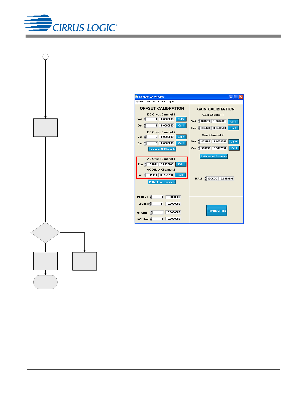
PERFORM AC OFFSET AND READ IRMS
Note: AC offset is only required when IRMS measurements are needed with high dynamic range
(only helpful at very low input levels).AC Offset Calibration Flow Diagram on page 44
SET SAMPLE COUNT
(See Figure 32.)
SDI = 0x90 0x73 0x000FA0 Write SampleCount (page 16, register 51)
SDO = 0xFF 0xFF 0xFFFFFF (4000)
SDI = 0x90 0x33 0xFFFFFF Read SampleCount (page 16, register 51)
SDO = 0xFF 0xFF 0x000FA0 (4000)
Figure 32. Setup Window
READ POWER REGISTERS
(See Figure 33.)
Gain Calibration, Channels 1 and 2, Voltage
SDI = 0x90 0x23 0xFFFFFF Read V1GAIN (page 16, register 35)
SDO = 0xFF 0xFF 0x3C1078 (0.9385054)
SDI = 0x90 0x2A 0xFFFFFF Read V2GAIN (page 16, register 42)
SDO = 0xFF 0xFF 0x3C1751 (0.9389233)
Gain Calibration, Channels 1 and 2, Current
SDI = 0x90 0x21 0xFFFFFF Read I1GAIN (page 16, register 33)
SDO = 0xFF 0xFF 0x1A77A0 (0.4135514)
SDI = 0x90 0x28 0xFFFFFF Read I2GAIN (page 16, register 40)
SDO = 0xFF 0xFF 0x1A78C4 (0.413621)
Offset Calibration, Channels 1 and 2, Current
SDI = 0x90 0x25 0xFFFFFF Read I1ACOFF (page 16, register 37)
SDO = 0xFF 0xFF 0x000000 (0)
SDI = 0x90 0x2C 0xFFFFFF Read I2ACOFF (page 16, register 44)
SDO = 0xFF 0xFF 0x000000 (0)
Offset Calibration, Channels 1 and 2, Active Power Offset
SDI = 0x90 0x24 0xFFFFFF Read P1OFF (page 16, register 36)
SDO = 0xFF 0xFF 0x000000 (0)
SDI = 0x90 0x2B 0xFFFFFF Read P2OFF (page 16, register 43)
SDO = 0xFF 0xFF 0x000000 (0)
Offset Calibration, Channels 1 and 2, Reactive Power Offset
SDI = 0x90 0x26 0xFFFFFF Read Q1OFF (page 16, register 38)
SDO = 0xFF 0xFF 0x000000 (0)
SDI = 0x90 0x2D 0xFFFFFF Read Q2OFF (page 16, register 45)
SDO = 0xFF 0xFF 0x000000 (0)
AN366REV2 37
Page 38

AN366
SET SCAL E REGIST ER
0.6
13
FULL LOAD
AVAILABLE ?
YES
NO
14 15
Figure 33. Calibration Window
CHECK IF FULL LOAD IS AVAILABLE
PC/Controller knows if full load or partial load set. The following step is not require if full
load is used.
(See Figure 34.)
SDI = 0x92 0x7F 0x4CCCCC Write Scale 0.6
SDO = 0xFF 0xFF 0xFFFFFF
SDI = 0x92 0x3F 0xFFFFFF Read Scale 0.6
SDO = 0xFF 0xFF 0x4CCCCC
38 AN366REV2
Figure 34. Calibration Window
Page 39

COMPUTE
CALIBR ATED
REGISTER
CHECKSUM
CALIBRATI ON
COMPLETE
STORE
CALIBRATI ON
CONSTANTS &
CHECKSUM
14 15
AN366
COMPUTE CALIBRATED REGISTER CHECKSUM
The register checksum is computed each time a conversion is completed (Single or Continuous). If no register have changed the user needs only read the checksum register after
prior conversion. But if a register has been updated (Scale for example) then the user must
perform another conversion before the read (see Figure 35).
If register(s) changed since conversion (SCALE changed), then perform single conversion
first, then read checksum:
SDI = 0xD4 Single Conversion Command (Optional)
SDO = 0xFF
SDI = 0x90 0x01 0xFFFFFF Read Checksum (Page 16, Register 1)
SDO = 0xFF 0xFF 0xF40578
Figure 35. Setup Window and Conversion Window
STORE CALIBRATION CONSTANTS & CHECKSUM
Write to MCU Flash all the calibration constants and checksum.
AN366REV2 39
Page 40

APPLY VOLTAGE
TO SOURCE &
60º LAGGING
LOAD
PF=0.5
FROM MAIN
FLOW
Tsettle =
2000ms
SampleCount
(N) = 16,000
Shown
In
Main
Flow
1
START
CONTINUOUS
CONVERSI ON
0xD5
Current
Voltag e
AN366
6.2.1 Phase Compensation Flow Diagram
The following flow diagram shows the implemented of phase compensation using the CDB5484U and a PC
as the controller. The MTE Meter Test Equipment source is used to provide the source voltage and load current
with a 60º phase shift (PF = 0.5). Each step of the flow shows the CDB5484 GUI screen capture of execution
and reading results. The register writes and reads are all identified for easy compares to the GUI screen
APPLY VOLTAGE AND 60* LAGGING LOAD TO SOURCE
(See Figure 36.)
.
Figure 36. Meter Test Equipment
40 AN366REV2
Page 41

AN366
READ PF
2
1
CALCULATE
PHASE
OFF SET =
arccos(PF)-60º
RESOLUTION
MULTIPLIER
0.008789 (50Hz)
0.010547 @ 60Hz
STOP
CONVERSIONS
0xD8
Shown
In
Main
Flow
STOP CONVERSIONS
(See Figure 37.)
SDI = 0x90 0x15 0xFFFFFF Read PF1 (page 16, register 21)
SDO = 0xFF 0xFF 0x410F40 (0.508278)
SDI = 0x90 0x19 0xFFFFFF Read PF2 (page 16, register 25)
SDO = 0xFF 0xFF 0x4106A8 (0.5080157)
For 1 to Count {
PF1SUM = PF1SUM + PF1
PF2SUM = PF2SUM + PF2}
Figure 37. Conversion Window
PF1AVG = PF1SUM ÷ Count
PF2AVG = PF1SUM ÷ Count
PHASE1_OFFSET = ARCCOS(0.5083238) - 60º = -0.55224327
PHASE2_OFFSET = ARCCOS(0.5085984) - 60º = -0.57051489
Use this constant stored from PC/Controller memory in following calculations.
AN366REV2 41
Page 42

-8.99º <
PHASE OFF SET
< +8.99º ? (50Hz)
PHASE OFF SET
NEGAT IVE?
-512 · 0.008789 <
PHASE OFF SET
< 0 (50Hz)
?
FINE
COMPENSAT ION
(F PCC) = -PHASE
OFFSET ÷
0.008789 (50Hz)
SET COAR SE
COMPENSAT ION
(CPCC = 01)
1 OWR on I
PHASE OFF SET =
PHASE OFF SET +
4.5º (50Hz)
±10.79º @ 60Hz
0 to 512 · 0.010547 @ 60Hz
5.4º @ 60Hz
0.010547 @ 60Hz
FAIL
METER
2
YES
NO
YES
NO
3
YES
Exam pl e Location
0º
Before Calibration V is delayed from I
Delay added to I
8.99º @ 50Hz
10.79 º @ 60Hz
4.5º @ 50Hz
5.4º @ 60Hz
-4.5º @ 50Hz
-5.4º @ 60Hz
-8 . 99 º @ 50H z
-10 .79 º @ 60 Hz
AN366
PHASE OFFSET
PC/Controller test for phase calibration range meet or fail meter. This example shows negative phase offset.
PHASE OFFSET
PC/Controller test for coarse phase calibration range.
When > 1 OWR, PC/Controller calculates Coarse Compensation
PC/Controller calculates Fine Compensation
CPCC1=0, FPCC1 = 62, CPCC2=0, FPCC2 = 64
SDI = 0x80 0x45 0x007C40 Write Phase Comp (page 0, register 69)
SDO = 0xFF 0xFF 0xFFFFFF
SDI = 0x80 0x05 0xFFFFFF Write Phase Comp (page 0, register 69)
SDO = 0xFF 0xFF 0x007C40
Figure 38. Negative Phase Offset
CPCC1 = 0
CPCC2 = 0
FPCC1 = -(-0.55224327) / 0.008789 @ 50Hz = 62,
FPCC2 = -(-0.57051489) / 0.008789 @ 50Hz = 64,
42 AN366REV2
Page 43

AN366
PHASE COMPENSATION COMPLETE
(RETURN CPCC & FPCC to MAIN)
ACCUMULATE MULTIPLE
PF READIN G AND
CONFIRM PF = 0.5
3
ACCUMULATE MULTIPLE PF READING AND CONFIRM
(See Figure 39.)
SDI = 0x90 0x15 0xFFFFFF Read PF1 (page 16, register 21)
SDO = 0xFF 0xFF 0x410F40 (0.508278)
SDI = 0x90 0x19 0xFFFFFF Read PF2 (page 16, register 25)
SDO = 0xFF 0xFF 0x4106A8 (0.5080157)
For 1 to Count {
PF1SUM = PF1SUM + PF1
PF2SUM = PF2SUM + PF2}
PF1AVG = PF1SUM ÷ Count
PF2AVG = PF1SUM ÷ Count
Figure 39. Conversion Window
43
Page 44

FROM MAIN
FLOW
CLEAR DRDY
REMOVE
LOAD CURRENT
Tsettle = 2000
SampleCount
N = 16000
Shown
In
Main
Flow
1
AN366
6.2.2 AC Offset Calibration Flow Diagram
The following flow diagram shows the implemented of AC offset calibration using the CDB5484U and a PC
as the controller. The MTE Meter Test Equipment source is used to provide the source voltage and no load
current. Each step of the flow shows the CDB5484 GUI screen capture of execution and reading results.
The register writes and reads are all identified for easy compares to the GUI screen.
REMOVE LOAD CURRENT
(See Figure 40.)
Figure 40. Meter Test Equipment
CLEAR DRDY in INTERRUPT STATUS
SDI = 0x80 0x57 0xFFFFFF Write INT STATUS DRDY
SDO = 0xFF 0xFF 0x800000 (Set DRDY INT) (page 0, register 23)
44
Page 45

SEND AC
OFFSET
CALIBRATION
0xF6
DRDY
SET ?
YES
NO
1
2
AN366
SEND AC OFFSET CALIBRATION
(See Figure 41.)
SDI = 0xF6 Write AC Offset Calibration – All Channels
SDO =0xFF
Figure 41. Calibration Window
DRDY SET?
SDI = 0x80 0x17 0xFFFFFFRead INT STATUS DRDY (page 0, register 23)
SDO =0xFF 0xFF 0x4XXXXX (DRDY not Set)
SDI = 0x80 0x17 0xFFFFFFRead INT STATUS DRDY (page 0, register 23)
SDO =0xFF 0xFF 0xCXXXXX (DRDY Set)
45
Page 46
AN366
CHECK
INPUT
OR
FAIL
RETURN
IACOFF
to
MAIN FLOW
IACOFF = 0?
AC OFFSET
CALIBR ATION
COMPLETE
NO
YES
READ IRMS,
IACOFF
2
READ POWER REGISTERS
Reading IRMS is shown in main flow (see Figure 42).
SDI = 0x90 0x25 0xFFFFFF Read I1ACOFF (page 16, register 37)
SDO = 0xFF 0xFF 0x050704 (0.0392766)
SDI = 0x90 0x2C 0xFFFFFF Read I2ACOFF (page 16, register 44)
SDO = 0xFF 0xFF 0x049959 (0.0359298)
46
Figure 42. Conversion Window
PC/Controller tests for change in IACOFF register to check for success.
6.2.3 DC Offset Calibration Flow Diagram
The implemented of DC offset calibration follows the same structure as AC offset except that the voltage
and current source are both zero. The high pass filters must not be enabled and instead of sending AC Calibration command (F6), the DC Calibration command is sent (E6). Refer to the main flow for reading the DC
offset registers.
Page 47

FROM MAIN
FLOW
CLEAR DRDY
APPLY FU LL
SCALE VOLT AGE
AND Z ERO LOAD
CURRENT
DRDY
SET?
TSETTLE = 2000
Sample Count
N = 16000
Shown
In
Main
Flow
NO
YES
1
START
CONTINUOUS
CONVERT
0xD5
AN366
6.2.4 No Load Offset Compensation Flow Diagram
The following flow diagram shows the implemented of no load power offset compensation using the
CDB5484U and a PC as the controller. The MTE Meter Test Equipment source is used to provide the source
voltage and no load current. Each step of the flow shows the CDB5484 GUI screen capture of execution
and reading results. The register writes and reads are all identified for easy compares to the GUI screen.
APPLY FULL SCALE VOLTAGE AND ZERO LOAD CURRENT
(See Figure 43.)
Figure 43. Meter Test Equipment
47
Page 48

1
ACCUMUL ATE
MULTIPLE
PAVG, QAVG
READIN GS
2
AN366
ACCUMULATE MULTIPLE PAVG, QAVG READINGS
(See Figure 44.)
Channels 1 and 2, Active Power
SDI = 0x90 0x05 0xFFFFFF Read P1AVG (page 16, register 5)
SDO = 0xFF 0xFF 0xFFFFFC (-0.00000048)
SDI = 0x90 0x0B 0xFFFFFF Read P2AVG (page 16, register 11)
SDO = 0xFF 0xFF 0xFFFFFF (-0.00000012)
Channels 1 and 2, Reactive Power
SDI = 0x90 0x0E 0xFFFFFF Read Q1AVG (page 16, register 14)
SDO = 0xFF 0xFF 0xFFFFFE (-0.00000024)
SDI = 0x90 0x10 0xFFFFFF Read Q2AVG (page 16, register 16)
SDO = 0xFF 0xFF 0xFFFFFC (-0.00000048)
Figure 44. Conversion Window
48
Page 49

AN366
RETURN
POFF
QOFF
to
MAIN FLOW
POWER OFF SET
CALIBRATION
COMPLETE
NEGAT E
QAVG
& STORE IN
QOFF
NEGAT E
PAVG
& STORE IN
POFF
2
SET POFF AND QOFF
Negate PAVG and QAVG registers and store in POFF and QOFF respectively (see
Figure 44).
SDI = 0x90 0x64 0xFFFFFF Write P1OFF (page 16, register 36)
SDO = 0xFF 0xFF 0x000003 (3.57628E-07)
SDI = 0x90 0x24 0xFFFFFF Read P1OFF (page 16, register 36)
SDO = 0xFF 0xFF 0x000003 (3.57628E-07)
SDI = 0x90 0x6B 0xFFFFFF Write P2OFF (page 16, register 43)
SDO = 0xFF 0xFF 0x000001 (1.19209E-07)
SDI = 0x90 0x2B 0xFFFFFF Read P2OFF (page 16, register 43)
SDO = 0xFF 0xFF 0x000001 (1.19209E-07)
SDI = 0x90 0x66 0xFFFFFF Write P1OFF (page 16, register 38)
SDO = 0xFF 0xFF 0x000002 (2.38419E-07)
SDI = 0x90 0x26 0xFFFFFF Read P1OFF (page 16, register 38)
SDO = 0xFF 0xFF 0x000002 (2.38419E-07)
SDI = 0x90 0x6D 0xFFFFFF Write P2OFF (page 16, register 45)
SDO = 0xFF 0xFF 0x000002 (2.38419E-07)
SDI = 0x90 0x2D 0xFFFFFF Read P2OFF (page 16, register 45)
SDO = 0xFF 0xFF 0x000002 (2.38419E-07)
Figure 45. Calibration Window
49
Page 50

Revision History
Contacting Cirrus Logic Support
For all product questions and inquiries contact a Cirrus Logic Sales Representative.
To find one nearest you go to http://www.cirrus.com
IMPORTANT NOTICE
Cirrus Logic, Inc. and its subsidiaries ("Cirrus") believe that the information contained in this document is accurate and reliable. However, the information is subject
to change without notice and is provided "AS IS" without warranty of any kind (express or implied). Customers are advised to obtain the latest version of relevant
information to verify, before placing orders, that information being relied on is current and complete. All products are sold subject to the terms and conditions of sale
supplied at the time of order acknowledgment, including those pertaining to warranty, indemnification, and limitation of liability. No responsibility is assumed by Cirrus
for the use of this information, including use of this information as the basis for manufacture or sale of any items, or for infringement of patents or other rights of third
parties. This document is the property of Cirrus and by furnishing this information, Cirrus grants no license, express or implied under any patents, mask work rights,
copyrights, trademarks, trade secrets or other intellectual property rights. Cirrus owns the copyrights associated with the information contained herein and gives consent for copies to be made of the information only for use within your organization with respect to Cirrus integrated circuits or other products of Cirrus. This consent
does not extend to other copying such as copying for general distribution, advertising or promotional purposes, or for creating any work for resale.
CERTAIN APPLICATIONS USING SEMICONDUCTOR PRODUCTS MAY INVOLVE POTENTIAL RISKS OF DEATH, PERSONAL INJURY, OR SEVERE PROPERTY OR ENVIRONMENTAL DAMAGE ("CRITICAL APPLICATIONS"). CIRRUS PRODUCTS ARE NOT DESIGNED, AUTHORIZED OR WARRANTED FOR USE
IN PRODUCTS SURGICALLY IMPLANTED INTO THE BODY, AUTOMOTIVE SAFETY OR SECURITY DEVICES, LIFE SUPPORT PRODUCTS OR OTHER CRITICAL APPLICATIONS. INCLUSION OF CIRRUS PRODUCTS IN SUCH APPLICATIONS IS UNDERSTOOD TO BE FULLY AT THE CUSTOMER'S RISK AND CIRRUS DISCLAIMS AND MAKES NO WARRANTY, EXPRESS, STATUTORY OR IMPLIED, INCLUDING THE IMPLIED WARRANTIES OF MERCHANTABILITY AND
FITNESS FOR PARTICULAR PURPOSE, WITH REGARD TO ANY CIRRUS PRODUCT THAT IS USED IN SUCH A MANNER. IF THE CUSTOMER OR CUSTOMER'S CUSTOMER USES OR PERMITS THE USE OF CIRRUS PRODUCTS IN CRITICAL APPLICATIONS, CUSTOMER AGREES, BY SUCH USE, TO FULLY
INDEMNIFY CIRRUS, ITS OFFICERS, DIRECTORS, EMPLOYEES, DISTRIBUTORS AND OTHER AGENTS FROM ANY AND ALL LIABILITY, INCLUDING ATTORNEYS' FEES AND COSTS, THAT MAY RESULT FROM OR ARISE IN CONNECTION WITH THESE USES.
Cirrus Logic, Cirrus, and the Cirrus Logic logo designs are trademarks of Cirrus Logic, Inc. All other brand and product names in this document may be
trademarks or service marks of their respective owners.
Revision Date Changes
REV1 APR 2012 Initial release.
REV 2 MAY 2012 Corrected typographical errors.
AN366
50
 Loading...