

Page 1
C
C
C
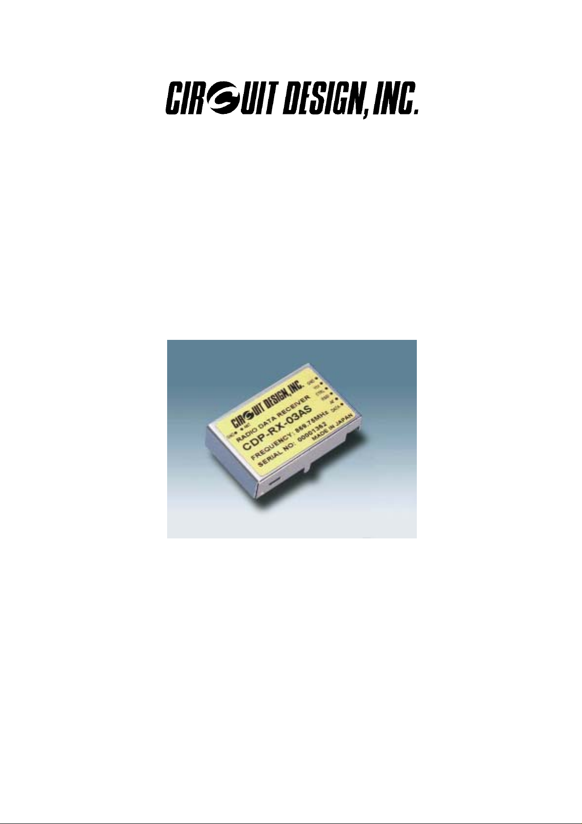
UHF FM-NARROW BAND RADIO DATA RECEIVER
D
D
D
P
P
P
-
R
-
R
-
R
CDP-RX-03AS
X
X
X
-
-
-
0
0
0
3
3
3
A
A
A
S
S
S
Operation Guide
Version 2.1 (Nov. 2001)
CIRCUIT DESIGN, INC.,
International Business Division
7557-1 Hotaka, Hotaka-machi, Minamiazumi, Nagano 399-8303. JAPAN
Tel: + +(0263)-82-1024 Fax: + +(0263)-82-1016
e-mail [email protected]
http://www.circuitdesign.co.jp
Page 2

CIRCUIT DESIGN, INC.
CONTENTS
GENERAL DESCRIPTION & FEATURES.................................3
OPERATION INSTRUCTIONS...................................................4
Supply voltage .....................................................................4
Data format...........................................................................4
Outputs.................................................................................. 4
Antennas .............................................................................. 5
SPECIFICATIONS........................................................................ 6
PIN DESCRIPTION...................................................................... 7
BLOCK DIAGRAM ..................................................................... 8
DIMENSIONS............................................................................... 9
TEST DATA.................................................................................10
CDP-RX-03AS UHF Radio Data Module Operation Guide
2
Page 3

GENERAL DESCRIPTION & FEATURES
Features
• 868-870 MHz & 433-434MHz UHF band. Compatible with European EN 300 220 standard
• Very small compact integrated device with robust metal housing
• FM narrow band modulation and high frequency stability
• Low current consumption, ideal for mobile application
• Control terminal for switching the power on/off
Applications
• Remote control system
• Telemetry system
• Social alarm system
• Security alarm system
• Paging system
General description
CIRCUIT DESIGN, INC.
The CDP-RX-03AS UHF FM-narrow band receiver is developed to cover a band plan of ERC
Recommendation on Short Range Device (SRD) in the range of 868-870MHz and 433434MHz ISM band. The receiver design is based on the double Super-heterodyne principle
with PLL control enabling high signal sensitivity, high selectivity, and high frequency stability
not achieved by simple SAW resonator receivers or other low cost designs.
Extensive filtering by an integrated unique SAW filter element enables operation in hazardous
areas where interference may be expected. Steadily increasing use of the available frequency
spectrum demands the application of narrow band systems for maximum operation reliability
and fairness to other users of the ISM band.
The CDP-RX-03AS receiver module is designed to match the CDP-TX-03S and the CDP-TX04S transmitter modules, though signals from other FM-narrow transmitters can be received
as well.
The receiver frequency must match with the transmitter frequency to enable reception. The
CDP-RX-03AS is designed for PCB mounting. A simple wire can be soldered to the antenna
input or the antenna can be printed on the PC board. Antenna of impedance matching with
each frequency should be used.
The receiver module has AF, DATA and RSSI signal out puts, and one control pin.
CDP-RX-03AS UHF Radio Data Module Operation Guide
3
Page 4

CIRCUIT DESIGN, INC.
OPERATION INSTRUCTIONS
Please read these instructions before you start using the CDP-RX03AS.
The CDP-RX-03AS is designed as a module that will be integrated into a user system. It is not
a ready-made product for private users. It can be regarded more like a special component for
part of an electronic system. The user needs basic knowledge about electronics. Special
knowledge about RF technology is helpful, but the most difficult parts are integrated into the
modules to enable easy operation. Some additional information is given here:
Supply voltage:
The CDP-RX-03AS receiver module contains a voltage regulator to guarantee stable
performance in the given range of supply voltage.
The design was made for operation with a battery. Supply voltage must be used within
specified voltage. The module shows unstable function with the voltage lower than specified.
If the voltage which connected to the Vcc (+) and Ground (-) terminal is beyond the maximum
voltage given in the technical specification or reversed, the module will be permanently
damaged. To enable a low minimum voltage, no internal circuit is used to prevent damage by
incorrect polarity.
If a higher supply voltage is available then a simple diode can be inserted in connection line to
the Vcc terminal to prevent damage by incorrect polarity. The diode must be rated for the
maximum supply current detailed in the technical specifications.
Data format:
Long intervals of HIGH or LOW bits should be avoided. Succeeding bits can be distorted in
their pulse width. If the sequence of HIGH or LOW bits is too long then there is possibility
that the logic level of the data output will change. The maximum pulse width for continuous
High and Low signal is 20msec (96bit) at 4800bps. The minimum pulse width is 208 us.
Maximum data rate is 4800bps.
It will be very helpful to have a 20 bits preamble (1010…) in front of the data to ensure
communication reliability.
In general, at higher data rates (4800 Baud) the internal signal is shaped into a slope and jitter
at the receiver data output increases.
Further advice can be given if the precise format of the data and system requirement is
notified to the dealer or directly to Circuit Design, Inc. Your inquiries and comments are
welcome .
Outputs:
At the receiver side 3 output (AF, DATA and RSSI) signals and one control terminal are
available.
AF output is the analog output from the FM detector circuit.
CDP-RX-03AS UHF Radio Data Module Operation Guide
4
Page 5

CIRCUIT DESIGN, INC.
The DATA output is a digital output. This is the signal after AF signal pass through band pass
filter and comparator. For simple FSK modulation of digital data, the DATA out terminal can
be used. The signal can be easily connected to other digital circuits.
The receiver has no internal mute circuit to avoid delays and achieve maximum sensitivity.
The AF and DATA output will show noise on the output when no signal is received. Valid data
signals can be detected by utilizing the RSSI output.
The third output is called RSSI. It is an indicator of the received signal strength. It can be used
to drive an external mute circuit.
Control terminal can be used to control Vcc supply for internal circuit.
Antennas:
Most important for effective data transmission is selection of a good antenna, and RF
grounding, both for the transmitter and the receiver. Without an antenna it is impossible to
transmit data over a long distance range.
The receiver has a simple antenna input pin. Any suitable UHF antenna can be connected to it.
The easiest way to connect an antenna to the CDP-RX-03AS is to solder an 8.6cm (868MHz)
or 17.3cm (434MHz) wire directly to the antenna input. If the receiving antenna is installed
away from the receiver module, a 50-Ohm Coax antenna wire can be used. The shielding of
the antenna wire should be soldered to the case near the antenna input of the CDP-RX-03AS.
It is possible, but not recommended to connect the receiver module and the antenna by a
connection on a PCB. This will decrease the receiver performance in most cases.
In most cases the following basic rules will help you.
• Connect an antenna with 50-Ohm impedance.
• Lambda/4 whip antenna length is approximately 17.3cm for 434MHz and 8.6cm for
868Mhz.
• Place the antenna vertically, straight up or down from the transmitter and receiver module.
• Do not cover the antenna with metal parts.
• The connection of the metal surface of the transmitter case to a larger metal part (ground
plane) will increase radiation efficiency. Such metal part should not be placed near the
antenna.
• The human body can have similar effects like metal objects. Pocket transmitters should be
taken in the hand and put in a position away from the body and pointed in the direction of
the receiver.
• Best range is achieved if the transmitter and receiver antenna have a direct visual
connection. Any object in between the transmitter and receiver antenna, and metallic
objects in particular, will decrease the range.
• The transmission is influenced by reflections of the transmitter signal on metallic surfaces
and building. There is possibility to have data error by overlaying the direct and reflected
signal.
CDP-RX-03AS UHF Radio Data Module Operation Guide
5
Page 6

CIRCUIT DESIGN, INC.
SPECIFICATIONS
RECEIVER: CDP-RX-03AS
RECEIVER TYPE Double Superheterodyne, PLL Controlled Fixed channel
FREQUENCIES Fixed channel 433.920, 434.075, 869.75MHz *
FREQUENCY STABILITY +/- 2.5kHz (-10 to +55 C) / 434MHz
+/- 3.0kHz (-10 to +55C) / 868MHz
PULSE WIDTH Min. 208uS Max.20mS
DATA RATE 100-4800bps FSK
SENSITIVITY -120 dBm / 434MHz (12dB/SINAD, CCITT filter )
-117 dBm / 868MHz (12dB/SINAD, CCITT filter )
SELECTIVITY +/-5 KHz at -6 dB point
DEMODULATION FM narrow
DISTORTION <5% at 1 KHz (AF output)
S/N RATIO 50 dB overall (AF output)
DATA OUTPUT Digital output, pulled up to Vcc (22 kohm)
OTHER OUTPUT RSSI, AF (-11 dBm typ. at Fm=1kHz /Fmod=+/-3kHz , 100kohm)
SUPPLY VOLTAGE 3.0 to 14V DC
SUPPLY CURRENT 18 mA ( Typ. )
I/O TERMINALS Ant, Gnd, Vcc, Data out, AF out, RSSI out, Power Control
SIZE & WEIGHT 36 x 26 x 8 mm (7.5cc), 12g
* Other frequency: Please contact to Circuit Design, Inc. distributor
Note: Above specifications are subject to change for improvement without prior notice.
CDP-RX-03AS UHF Radio Data Module Operation Guide
6
Page 7
CIRCUIT DESIGN, INC.
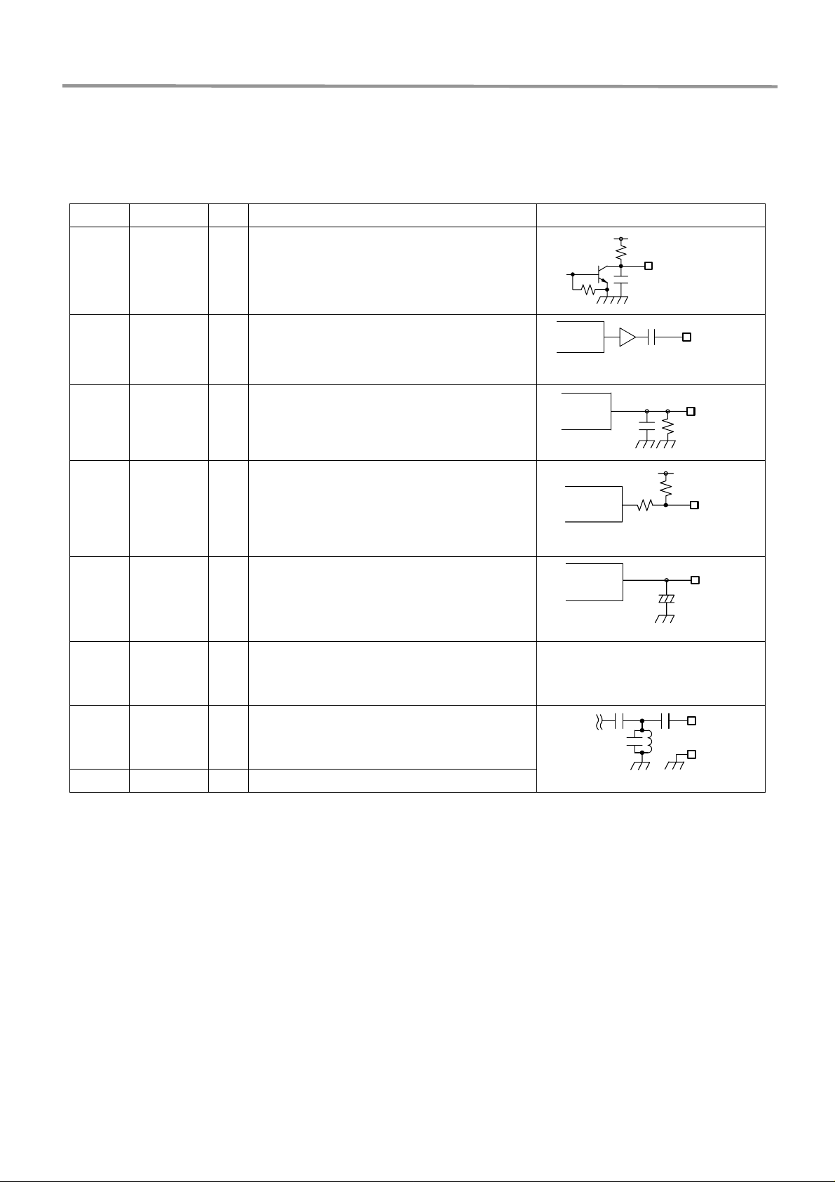
PIN DESCRIPTION
Pin-No. Pin-Name I/O Description Equivalent internal circuit
CN1-1 DATA O
The data signal output
The terminal is pulled up with resister
CN1-2 AF O
The AF signal output terminal
The signal output level is –11dBm typ.
(
Fm=1KHz /Fmod=+/-3KHz, 100Kohm)
AFOut
IF IC
Vcc
100 p
Lo w Pass Filter
22k
Pin
1uF
Pin
CN1-3 RSSI O
CN1-4 CTRL I
CN1-5 VCC -
CN1-6 GND -
CN2-1 ANT I
CN2-1 GND -
The receiving level output
The level indicate the strength of RF level
The power on/off control terminal. (Lo active)
The voltage which Vcc-1.8V or lower voltage
make the circuit active.
The power supply terminal
Operates on 3.0 to 14V
The ground
Connect to the ground of the control board.
The antenna terminal
Connect the antenna with 50 ohm impedance
The ground terminal for the antenna
RSSI
IF IC
Voltage Regulator
Voltage Regulator
Cont
Vin
103
100K
Vcc
10K
4.7u
Pin
56K
Pin
Pin
ANT
GND
CDP-RX-03AS UHF Radio Data Module Operation Guide
7
Page 8
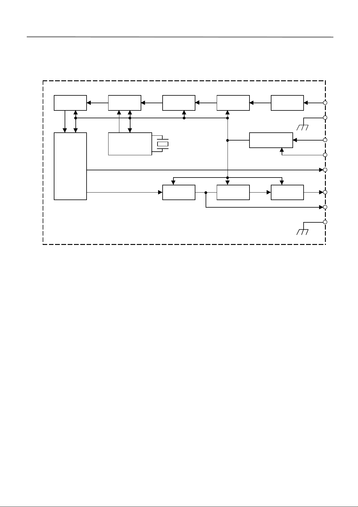
BLOCK DIAGRAM
BAND
BAND
CIRCUIT DESIGN, INC.
XTAL
FILTER
2nd MIX
/IF-AMP
/DEMOD.
MIXER
/IF-AMP
VCO/PLL
SAW
FILTER
PASS
RF-AMP
2.7V
DATA
DETECT
PASS
REGULATOR Vcc
BUFFER DATA
ANT
GND
CTRL
RSSI
AFOUT
GND
CDP-RX-03AS UHF Radio Data Module Operation Guide
8
Page 9
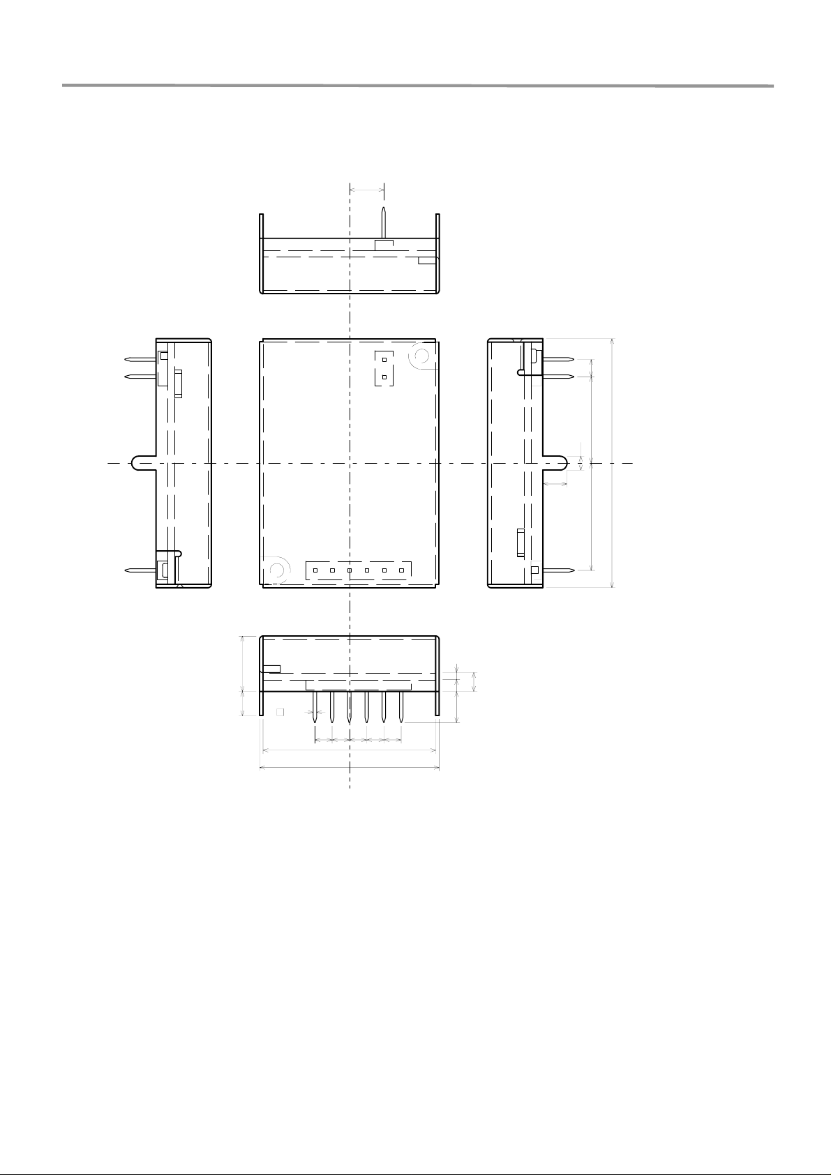
DIMENSIONS
CIRCUIT DESIGN, INC.
5.08
2
CN2
CN1
8.0
3.5
0.64
12 453
25
26
6
2.54
1
2.7
4.3
1
3.5
2.54
12.44
2
36
15.5
PIN CON ECTION
CN1-
1: D ATA
2: A F
3: RS SI
4: CT RL
5: V cc
6: G ND
CN2- 1: ANT
2: GND
CDP-RX-03AS UHF Radio Data Module Operation Guide
9
Page 10
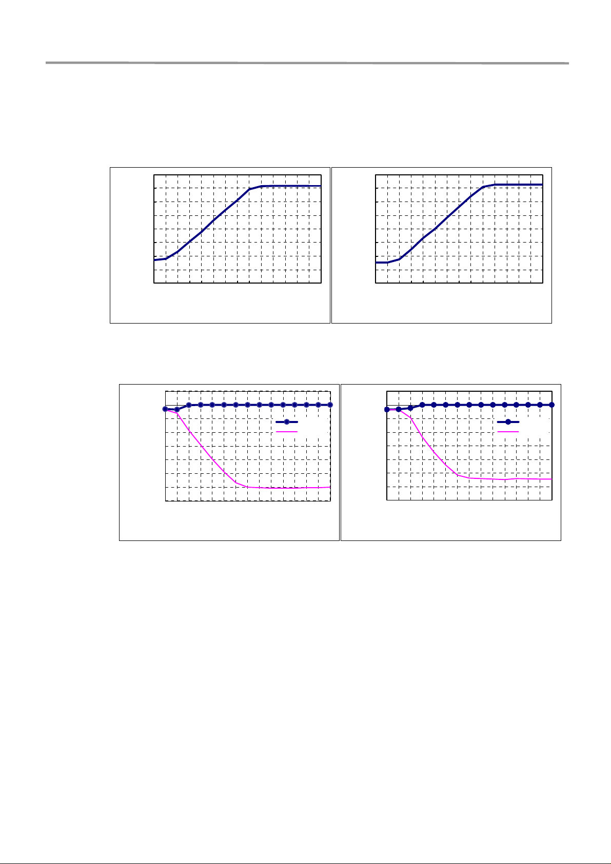
TEST DATA
RSSI (V)
CIRCUIT DESIGN, INC.
1.60
1.40
1.20
1.00
0.80
RSSI(V)
0.60
0.40
0.20
0.00
-140 -120 -100 -80 -60 -40 -20 0
RF-INPUT(dBm)
1.60
1.40
1.20
1.00
0.80
RSSI(V)
0.60
0.40
0.20
0.00
-140 -120 -100 -80 -60 -40 -20 0
RF-INPUT(dBm)
434MHz 868MHz
SIGNAL/NOISE RATIO (dB)
10.0
0.0
-10.0
-20.0
-30.0
-40.0
RATIO(dB)
-50.0
-60.0
-70.0
-140 -120 -100 -80 -60 -40 -20 0
RF-INPUT(dBm)
S+N+D
N
10.0
0.0
-10.0
-20.0
-30.0
-40.0
RATIO(dB)
-50.0
-60.0
-70.0
-140 -120 -100 -80 -60 -40 -20 0
RF-INPUT(dBm)
S+N+D
N
434MHz 868MHz
CDP-RX-03AS UHF Radio Data Module Operation Guide
10
 Loading...