

Page 1

6121 Baker Road,
Suite 108
Minnetonka, MN 55345
www.chtechnology.com
Phone (952) 933-6190
Fax (952) 933-6223
1-800-274-4284
Thank you for downloading this document from C&H Technology, Inc.
Please contact the C&H Technology team for the following questions -
Technical
Application
Assembly
Availability
Pricing
Phone – 1-800-274-4284
E-Mail – sales@chtechnology.com
www.chtechnology.com - SPECIALISTS IN POWER ELECTRONIC COMPONENTS AND ASSEMBLIES - www.chtechnology.com
Page 2
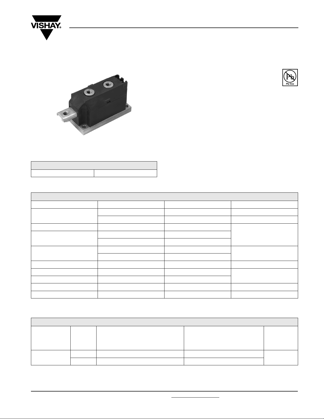
Fast Thyristor/Diode and Thyristor/Thyristor
(MAGN-A-PAK
MAGN-A-PAK
PRODUCT SUMMARY
I
T(AV)
TM
200 A
VSK.F200..P Series
Vishay High Power Products
TM
Power Modules), 200 A
FEATURES
• Fast turn-off thyristor
• Fast recovery diode
• High surge capability
• Electrically isolated baseplate
• 3500 V
• Industrial standard package
• Lead (Pb)-free
• Designed and qualified for industrial level
DESCRIPTION
This series of MAGN-A-PAKTM modules are intended
for applications such as self-commutated inverters, DC
choppers, electronic welders, induction heating and others
where fast switching characteristics are required.
isolating voltage
RMS
RoHS
COMPLIANT
MAJOR RATINGS AND CHARACTERISTICS
SYMBOL CHARACTERISTICS VALUES UNITS
I
T(AV)
I
T(RMS)
I
TSM
2
I
t
2
I
√t 2900 kA2√s
t
q
t
rr
V
DRM/VRRM
T
J
T
C
50 Hz 7600
60 Hz 8000
50 Hz 290
60 Hz 265
Range - 40 to 125 °C
200 A
85 °C
444
20/25
2
up to 1200 V
ELECTRICAL SPECIFICATIONS
VOLTAGE RATINGS
, MAXIMUM REPETITIVE
BLOCKING VOLTAGE
V
V
, MAXIMUM NON-REPETITIVE
RSM
PEAK REVERSE VOLTAGE
V
TYPE NUMBER
VSK.F200-
V
RRM/VDRM
VOLTAGE
CODE
08 800 800
12 1200 1200
PEAK REVERSE AND OFF-STATE
A
kA2s
µs
I
RRM/IDRM
AT TJ = 125 °C
mA
50
Document Number: 94422 For technical questions, contact: ind-modules@vishay.com
Revision: 03-Jun-08 1
www.vishay.com
Page 3
VSK.F200..P Series
Vishay High Power Products
Fast Thyristor/Diode and Thyristor/Thyristor
(MAGN-A-PAKTM Power Modules), 200 A
CURRENT CARRYING CAPABILITY
I
FREQUENCY UNITS
180° el
TM
180° el
50 Hz 380 560 630 850 2460 3180
400 Hz 460 690 710 1060 1570 2080
2500 Hz 310 450 530 760 630 860
5000 Hz 250 360 410 560 410 560
10 000 Hz 180 280 300 410 - -
Recovery voltage V
r
Voltage before turn-on V
d
50 50 50 50 50 50
80 % V
DRM
80 % V
Rise of on-state current dI/dt 5050----A/µs
Case temperature 85 60 85 60 85 60 °C
Equivalent values for RC circuit 10/0.47 10/0.47 10/0.47 Ω/µF
ON-STATE CONDUCTION
PARAMETER SYMBOL TEST CONDITIONS VALUES UNITS
Maximum average on-state current
at case temperature
Maximum RMS on-state current I
Maximum peak, one-cycle
non-repetitive on-state,
surge current
2
Maximum I
Maximum I
t for fusing I2t
2
√t for fusing I2√t t = 0.1 to 10 ms, no voltage reapplied 2900 kA2√s
Low level value or threshold voltage V
High level value of threshold voltage V
Low level value on-state slope resistance r
High level value on-state slope resistance r
Maximum on-state voltage drop V
Maximum holding current I
Maximum latching current I
I
T(AV)
T(RMS)
I
TSM
T(TO)1
T(TO)2
t1
(I > π x I
t2
TM
H
L
180° conduction, half sine wave
As AC switch 444
t = 10 ms
t = 8.3 ms 8000
t = 10 ms
t = 8.3 ms 6700
t = 10 ms
t = 8.3 ms 265
t = 10 ms
t = 8.3 ms 187
(16.7 % x π x I
T
= TJ maximum
J
(I > π x I
T(AV)
(16.7 % x π x I
= TJ maximum
T
J
T(AV)
No voltage
reapplied
100 % V
reapplied
No voltage
reapplied
100 % V
reapplied
< I < π x I
T(AV)
< I < π x I
< I < π x I
T(AV)
< I < π x I
T(AV)
T(AV)
Ipk = 600 A, TJ = TJ maximum, tp = 10 ms sine pulse 1.73 V
TJ = 25 °C, IT > 30 A 6000
TJ = 25 °C, VA = 12 V, Ra = 6 Ω, Ig = 1A 1000
DRM
I
TM
100 µs
80 % V
DRM
I
TM
200 A
85 °C
7600
RRM
RRM
T(AV)
Sinusoidal
half wave,
initial T
),
= 125 °C
J
6400
290
205
1.18
), TJ = TJ maximum 1.25
),
T(AV)
0.74
), TJ = TJ maximum 0.70
A
V
A
kA2s
V
mΩ
mA
www.vishay.com For technical questions, contact: ind-modules@vishay.com
Document Number: 94422
2 Revision: 03-Jun-08
Page 4

VSK.F200..P Series
Fast Thyristor/Diode and Thyristor/Thyristor
Vishay High Power Products
(MAGN-A-PAKTM Power Modules), 200 A
SWITCHING
PARAMETER SYMBOL TEST CONDITIONS
Maximum non-repetitive rate of rise dI/dt
Maximum recovery time t
Maximum turn-off time t
rr
q
Gate drive 20 V, 20 Ω, t
T
= 25 °C
J
ITM = 350 A, dI/dt = - 25 A/µs, VR = 50 V, TJ = 25 °C 2
I
= 750 A; TJ = TJ maximum; dI/dt = - 25 A/µs;
TM
V
= 50 V; dV/dt = 400 V/µs linear to 80 % V
R
≤ 1 ms, VD = 80 % V
r
DRM
DRM
BLOCKING
PARAMETER SYMBOL TEST CONDITIONS VALUES UNITS
Maximum critical rate of rise of
off-state voltage
RMS insulation voltage V
Maximum peak reverse and off-state
leakage current
dV/dt T
INS
,
I
RRM
I
DRM
= 125 °C, exponential to 67 % V
J
DRM
50 Hz, circuit to base, TJ = 25 °C, t = 1 s 3000 V
TJ = 125 °C, rated V
DRM/VRRM
applied 50 mA
TRIGGERING
PARAMETER SYMBOL TEST CONDITIONS VALUES UNITS
Maximum peak gate power P
Maximum peak average gate power P
Maximum peak positive gate current I
Maximum peak negative gate voltage -V
Maximum DC gate current required to trigger I
DC gate voltage required to trigger V
DC gate current not to trigger I
DC gate voltage not to trigger V
GM
G(AV)
GM
GT
GT
GD
GD
f = 50 Hz, d% = 50 60
TJ = 125 °C, f = 50 Hz, d% = 50 10
TJ = 125 °C, tp ≤ 5 ms
GT
TJ = 25 °C, V
TJ = 125 °C, rated V
12 V, Ra = 6
ak
DRM
applied
VALUES
KJ
,
20 25
UNITS
800 A/µs
µs
1000 V/µs
W
10 A
5V
200 mA
3V
20 mA
0.25 V
THERMAL AND MECHANICAL SPECIFICATIONS
PARAMETER SYMBOL TEST CONDITIONS VALUES UNITS
Maximum junction operating
temperature range
Storage temperature range T
Maximum thermal resistance,
junction to case per junction
Maximum thermal resistance,
case to heatsink per module
MAP to heatsink
Mounting torque ± 10 %
busbar to MAP
R
R
T
J
Stg
thJC
thC-hs
DC operation 0.125
Mounting surface flat, smooth and greased 0.025
A mounting compound is recommended. The torque
should be rechecked after a period of 3 hours to
allow for the spread of the compound. Use of cable
lugs is not recommended, busbar should be used
Approximate weight
and restrained during tightening. Threads must be
lubricated with a compound.
Document Number: 94422 For technical questions, contact: ind-modules@vishay.com
Revision: 03-Jun-08 3
- 40 to 125
- 40 to 150
4 to 6
(35 to 53)
500 g
17.8 oz.
www.vishay.com
°C
K/W
N · m
(lbf · in)
Page 5

VSK.F200..P Series
Vishay High Power Products
Fast Thyristor/Diode and Thyristor/Thyristor
(MAGN-A-PAKTM Power Modules), 200 A
ΔR
Note
• Table shows the increment of thermal resistance R
CONDUCTION
thJC
CONDUCTIONS ANGLE SINUSOIDAL CONDUCTION RECTANGULAR CONDUCTION UNITS
180° 0.009 0.006
120° 0.10 0.011
90° 0.014 0.015
60° 0.020 0.020
30° 0.32 0.033
when devices operate at different conduction angles than DC
thJC
130
120
110
100
90
80
70
60
Maximum Allowable Case Temperature (°C)
0 40 80 120 160 200 240
VSK.F200. . Serie s
R ( D C ) = 0. 12 5 K/ W
thJC
Cond uc tion A ngle
30°
60°
90°
120°
Average On-state Current (A)
180°
350
300
250
200
150
100
50
0
Maximum Average On-state Power Loss (W)
180°
120°
90°
60°
30°
RM S Li m i t
Conduc tion Angle
VSK.F200. . Series
Pe r Ju nc t io n
T = 12 5 ° C
J
0 40 80 120 160 200
Average On-state Current (A)
K/W
Fig. 1 - Current Ratings Characteristics
130
120
110
100
90
80
70
60
Maximum Allowable Case Temperature (°C)
0 50 100 150 200 250 300 350
VSK.F200.. Se rie s
R (DC) = 0.125 K/W
thJC
Conduction Period
30°
60°
90°
120°
180°
Average On-state Current (A)
Fig. 2 - Current Ratings Characteristics
DC
Fig. 3 - On-State Power Loss Characteristics
500
450
400
350
300
250
200
150
100
50
Maximum Average On-state Power Lo ss (W)
DC
180°
120°
90°
60°
30°
RM S Li m i t
Conduction Period
VSK.F200.. Se ries
Pe r Ju nc t i on
T = 12 5° C
0
0 50 100 150 200 250 300 350
Average On-state Current (A)
J
Fig. 4 - On-State Power Loss Characteristics
www.vishay.com For technical questions, contact: ind-modules@vishay.com
Document Number: 94422
4 Revision: 03-Jun-08
Page 6

VSK.F200..P Series
Fast Thyristor/Diode and Thyristor/Thyristor
(MAGN-A-PAKTM Power Modules), 200 A
7000
6000
5000
4000
Peak Half Sine Wave On-state Current (A)
3000
Number Of Equal Amplitude Half Cycle Current Pulses (N)
Fig. 5 - Maximum Non-Repetitive Surge Current
8000
7000
6000
5000
4000
Peak Half Sine Wa ve On-st ate Current (A)
3000
At Any Ra ted Load Condition And With
Rat ed V Applie d Follo wing Surg e.
RRM
VSK.F200.. Serie s
Pe r Ju n c t io n
110100
Maximum Non Rep etitive Surge Current
Versus Pulse Train Duration. Control
Of Co ndu c tion May Not Be Ma intaine d.
VSK.F200.. Series
Pe r Ju nc t io n
0.01 0.1 1
Pu lse Tr a in D ura t io n ( s)
Initia l T = 125°C
J
@ 6 0 Hz 0 .0 0 8 3 s
@ 5 0 Hz 0 .0 1 0 0 s
Ini t ial T = 125°C
No Vo ltage Re ap plied
Ra t e d V Re a p p l i e d
J
RRM
Vishay High Power Products
1
Steady State Value:
R = 0.125 K/W
thJC
(DC Ope ration)
thJC
0.1
0.01
VSK.F200.. Serie s
Pe r Ju n c t i o n
Tra nsient The rma l Imp eda nc e Z (K/W)
0.001
0.001 0.01 0.1 1 10 100
Sq u a r e W a v e P ul se D u ra t i o n ( s)
Fig. 8 - Thermal Impedance Z
320
300
280
260
240
220
200
180
160
140
120
100
80
10 20 30 40 50 60 70 80 90 100
Maximum Reverse Recovery Charge - Qrr (µC)
Rate Of Fa ll Of Forward Current - d i/ dt ( A/ µs)
I = 1000 A
TM
500 A
300 A
200 A
100 A
Characteristics
thJC
VSK.F200.. Serie s
T = 12 5 °C
J
Fig. 6 - Maximum Non-Repetitive Surge Current
10000
1000
T = 2 5 ° C
J
T = 1 2 5 ° C
J
VSK.F200.. Serie s
Instantaneous On-state Current (A)
100
1234567
Inst a nt an e ou s On -sta te Vol t ag e ( V)
Pe r J u nc t i o n
Fig. 7 - On-State Voltage Drop Characteristics
Fig. 9 - Reverse Recovery Charge Characteristics
180
150
120
90
60
30
Ma ximum Rev erse Re co ve ry Current - Irr (A)
10 20 30 40 50 60 70 80 90 100
Rate Of Fall Of Forward Current - di/dt (A/ µs)
I = 1000A
TM
500A
300A
200A
100A
VSK.F200.. Se ries
T = 12 5 °C
J
Fig. 10 - Reverse Recovery Current Characteristics
Document Number: 94422 For technical questions, contact: ind-modules@vishay.com
www.vishay.com
Revision: 03-Jun-08 5
Page 7

VSK.F200..P Series
Vishay High Power Products
1E4
150
400
1E3
5000
1E2
Peak On-stata Current (A)
1E1
1E1 1 E2 1E3 1E4
VSK.F200.. Series
Sinusoidal pulse
T = 85 °C
tp
1E4
VSK.F200.. Serie s
Tr a p e z o i d a l p u l s e
T = 8 5° C d i / d t 5 0 A / µ s
tp
C
1000
2500
C
Pu lse Ba se w id t h ( µs)
Sn u b b e r c i r c u i t
R = 10 o hm s
C = 0.47 µF
V = 80% V
Fast Thyristor/Diode and Thyristor/Thyristor
(MAGN-A-PAKTM Power Modules), 200 A
50 Hz
2500
5000
VSK.F200.. Seri es
s
s
D
DRM
1E4
Fig. 11 - Frequency Characteristics
1E1
E1 1 E2 1 E3 1 E4
Si n us o i d a l p u l se
tp
T = 6 0 ° C
C
VSK.F200.. Serie s
Trap ezoida l p ulse
tp
T = 8 5 °C d i / d t 1 0 0A / µ s
C
Pu lse Ba sew id t h (µ s)
1000
400
50 Hz
150
Snub ber c irc uit
R = 1 0 o h ms
s
C = 0.47 µF
s
V = 80% V
D
DRM
50 Hz
150
1E3
2500
5000
Peak O n-sta te C urre nt (A )
1E2
1 E1 1 E2 1 E3 1 E4
1000
400
Sn u b b e r c i r c u i t
R = 1 0 o h ms
s
C = 0.47 µF
s
V = 80% V
D
Pu lse Ba se w i dt h ( µs)
1E4
50 Hz
150
1E3
2500
5000
Peak On-state Current (A)
1E2
1E1 1E2 1E3 1E4
VSK.F200.. Se rie s
Trapezoidal pulse
T = 6 0 ° C d i / d t 5 0 A / µ s
tp
C
1000
400
Sn u b b e r c i r c u i t
R = 1 0 o h m s
s
C = 0.47 µF
s
V = 80% V
D
Pu lse Ba se w id t h (µ s)
DRM
1E1
1E4
E1 1 E2 1 E3 1 E4
Fig. 12 - Frequency Characteristics
DRM
1E1
1E4
E1 1 E2 1 E3 1 E4
2500
5000
Pu lse Ba sew id t h (µ s)
5000
VSK.F200.. Series
Tr a p e zo i d a l p u l se
T = 60°C di/ dt 100A/µ s
tp
C
150
400
1000
150
400
1000
2500
Pu lse Ba se w id t h (µ s)
50 Hz
Sn u b b e r c i r c u i t
R = 1 0 o h ms
s
C = 0.47 µF
s
V = 80% V
D
50 Hz
Snu bb er c irc uit
R = 10 o hm s
s
C = 0.47 µF
s
V = 80% V
DRM
D
DRM
Fig. 13 - Frequency Characteristics
www.vishay.com For technical questions, contact: ind-modules@vishay.com
Document Number: 94422
6 Revision: 03-Jun-08
Page 8

VSK.F200..P Series
Fast Thyristor/Diode and Thyristor/Thyristor
(MAGN-A-PAKTM Power Modules), 200 A
1E4
10 jou les pe r p ulse
5
2.5
1
1E3
1E2
VSK.F200.. Se ries
Peak On-sta te Current (A)
1E1
1E11E21E31E4
tp
Si n us o i d a l p u l se
0.5
0.25
0.1
0.05
Pu lse Ba se w id t h ( µs)
Fig. 14 - Maximum On-State Energy Power Loss Characteristics
100
Rectangular gate pulse
a) Recommended load line for
rated d i/d t : 10V, 10ohms
b) Recommended load line for
<=30% rated di/dt : 10V, 20ohms
10
1
VGD
Inst a nta n e ous Ga te Vol t ag e (V)
0.1
0.01 0.1 1 10 100
IGD
1E4
(b)
T
Tj = 1 25 ° C
j=25 °C
In st a n t a n eo u s G a t e C ur re n t (A )
Fig. 15 - Gate Characteristics
Vishay High Power Products
0.5
0.25
0.1
0.05
VSK.F200.. Se ries
Trapezoidal pulse
di/dt 50A/µs
tp
E1 1 E2 1 E3 1 E4
1E1
Pu lse Ba se w i dt h ( µs)
(1) PGM = 8W, tp = 25ms
(2) PGM = 20W, tp = 1ms
(3) PGM = 40W, tp = 5ms
(4) PGM = 80W, tp = 2.5ms
(a)
Tj= - 4 0 ° C
(1)
(2)
(3)
VSK.F200.. Series Frequency Limited by PG(AV)
1
(4)
10 jou les per p ulse
5
2.5
ORDERING INFORMATION TABLE
Device code
Note
• To order the optional hardware go to www.vishay.com/doc?95172
Document Number: 94422 For technical questions, contact: ind-modules@vishay.com
Revision: 03-Jun-08 7
VSK T F 200 - 12 H K P
324
1 - Module type
2 - Circuit configuration
3
- Fast SCR
4
- Current rating: I
x 10 rounded
T(AV)
5 - Voltage code x 100 = V
6 - dV/dt code: H ≤ 400 V/µs
7 -tq code: K ≤ 20 µs
J ≤ 25 µs
8 - Lead (Pb)-free
51
678
(see Voltage Ratings table)
RRM
www.vishay.com
Page 9

VSK.F200..P Series
Vishay High Power Products
Fast Thyristor/Diode and Thyristor/Thyristor
(MAGN-A-PAKTM Power Modules), 200 A
CIRCUIT CONFIGURATION
+
~
-
VSKLF...
~
+
-
VSKUF...
~
+
-
+
-
-
G1
K1
+
-
-
G2
VSKVF...
K2
LINKS TO RELATED DOCUMENTS
VSKKF...
-
-
+
+
+
+
G1
G2
K2
K1
+
-
-
~
+
-
G2
K2
VSKHF...
~
+
-
G1
K1
VSKTF...
~
+
-
G1
K1
Dimensions http://www.vishay.com/doc?95086
G2
VSKNF...
+
-
-
K2
-
+
+
+
www.vishay.com For technical questions, contact: ind-modules@vishay.com
Document Number: 94422
8 Revision: 03-Jun-08
 Loading...