

Page 1

6121 Baker Road,
Suite 108
Minnetonka, MN 55345
www.chtechnology.com
Phone (952) 933-6190
Fax (952) 933-6223
1-800-274-4284
Thank you for downloading this document from C&H Technology, Inc.
Please contact the C&H Technology team for the following questions -
Technical
Application
Assembly
Availability
Pricing
Phone – 1-800-274-4284
E-Mail – sales@chtechnology.com
www.chtechnology.com - SPECIALISTS IN POWER ELECTRONIC COMPONENTS AND ASSEMBLIES - www.chtechnology.com
Page 2
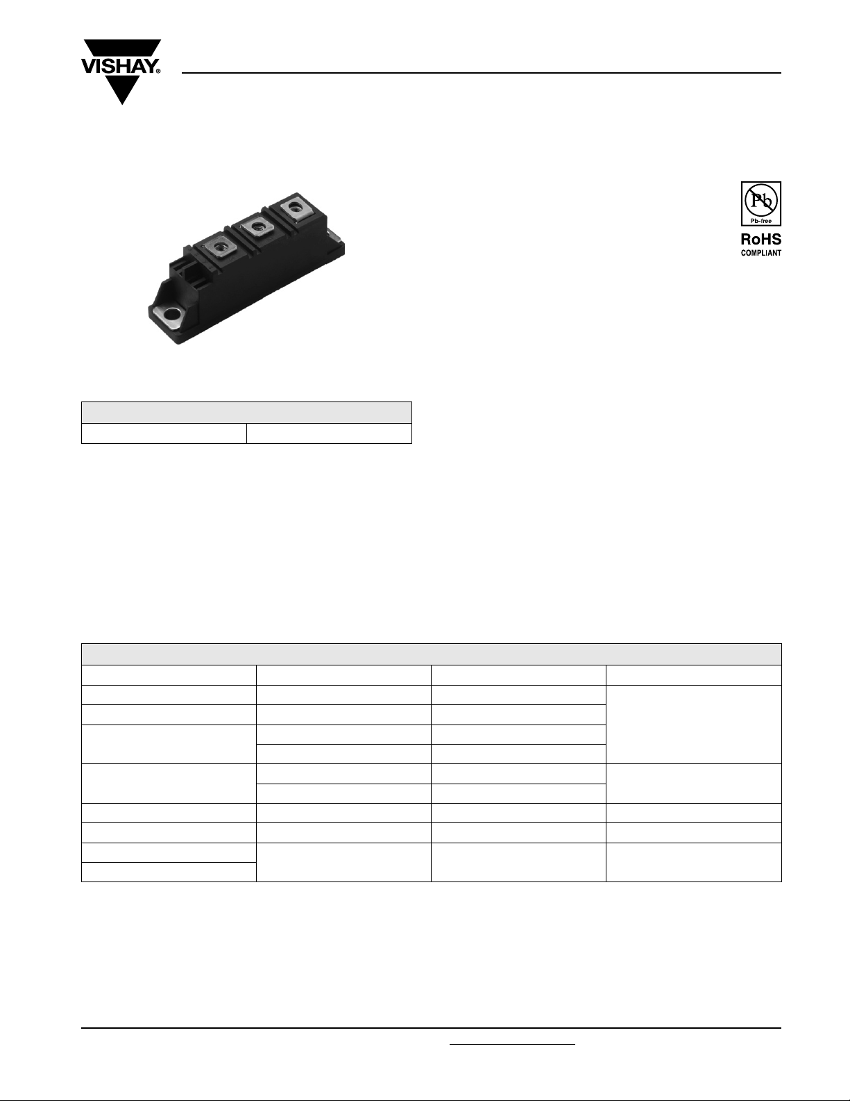
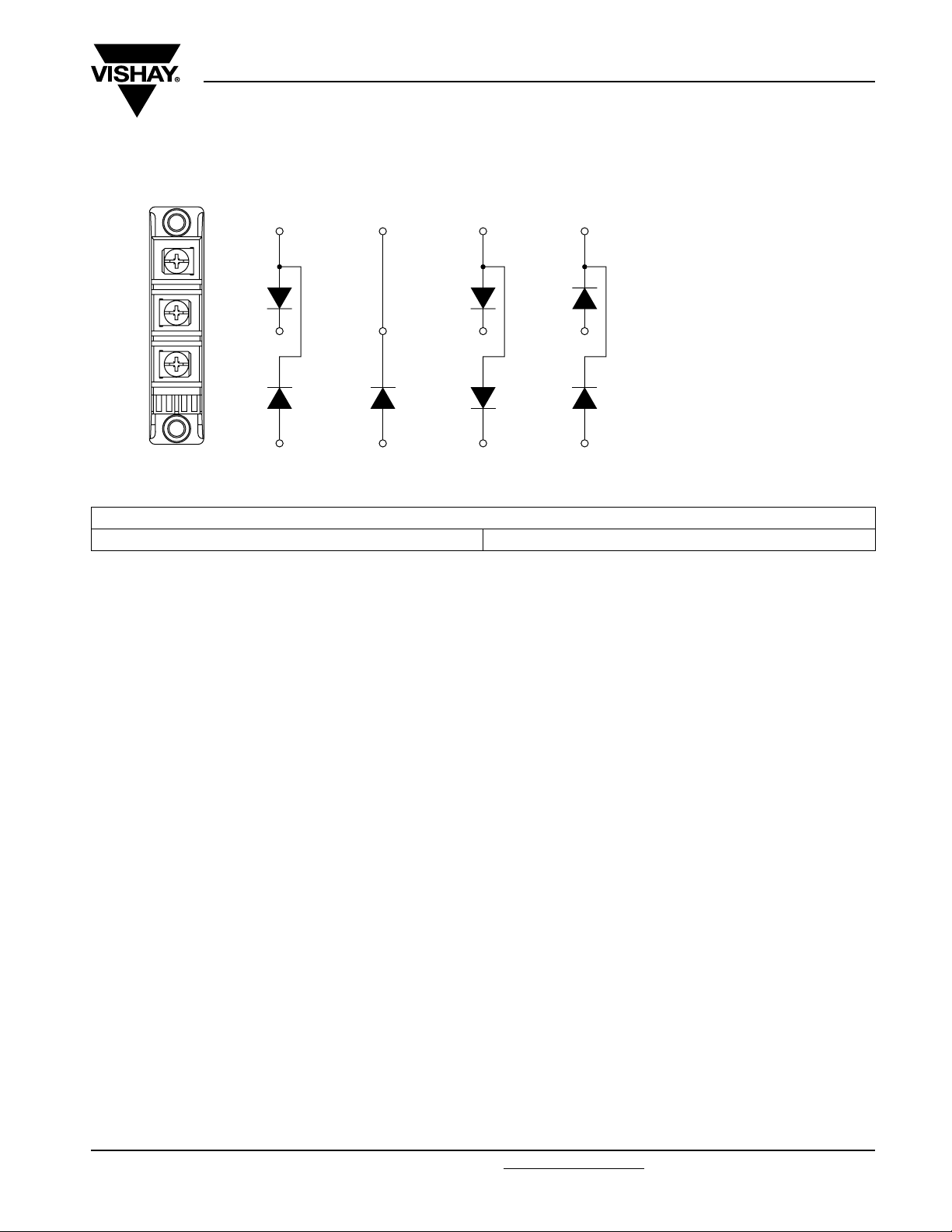
ADD-A-PAK Generation VII Power Modules
ADD-A-PAK
PRODUCT SUMMARY
I
F(AV)
Vishay High Power Products
Standard Diodes, 80 A
FEATURES
• High voltage
• Industrial standard package
• UL pending
isolating voltage
RMS
80 A
• 3500 V
• Low thermal resistance
• Totally lead (Pb)-free
• Designed and qualified for industrial level
BENEFITS
• Excellent thermal performances obtained by the usage of
exposed direct bonded copper substrate
• Up to 1600 V
VSK.71.. Series
• High surge capability
MECHANICAL DESCRIPTION
• Easy mounting on heatsink
The ADD-A-PAK generation VII, new generation of
ADD-A-PAK module, combines the excellent thermal
performances obtained by the usage of exposed direct
bonded copper substrate, with advanced compact simple
package solution and simplified internal structure with
minimized number of interfaces.
ELECTRICAL DESCRIPTION
These modules are intended for general purpose high
voltage applications such as high voltage regulated power
supplies, lighting circuits, temperature and motor speed
control circuits, UPS and battery charger.
MAJOR RATINGS AND CHARACTERISTICS
SYMBOL CHARACTERISTICS VALUES UNITS
I
F(AV)
I
F(RMS)
I
FSM
2
I
t
2
I
√t 112.5 kA2√s
V
RRM
T
J
T
Stg
110 °C 80
126
50 Hz 1500
60 Hz 1570
50 Hz 11.25
60 Hz 10.26
Range 400 to 1600 V
- 40 to 150 °C
A
kA2s
Document Number: 94626 For technical questions, contact: ind-modules@vishay.com
Revision: 17-Dec-08 1
www.vishay.com
Page 3
VSK.71.. Series
Vishay High Power Products
ADD-A-PAK Generation VII Power Modules
Standard Diodes, 80 A
ELECTRICAL SPECIFICATIONS
VOLTAGE RATINGS
V
, MAXIMUM NON-REPETITIVE
RSM
PEAK REVERSE VOLTAGE
V
TYPE NUMBER
VOLTAGE
CODE
V
, MAXIMUM REPETITIVE
RRM
PEAK REVERSE VOLTAGE
V
04 400 500
06 600 700
08 800 900
VSK.71
10 1000 1100
12 1200 1300
14 1400 1500
16 1600 1700
FORWARD CONDUCTION
PARAMETER SYMBOL TEST CONDITIONS VALUES UNITS
Maximum average forward current
at case temperature
Maximum RMS forward current I
Maximum peak, one-cycle forward,
non-repetitive surge current
2
Maximum I
Maximum I
t for fusing I2t
2
√t for fusing I2√t t = 0.1 ms to 10 ms, no voltage reapplied 112.5 kA2√s
Low level value of threshold voltage V
High level value of threshold voltage V
Low level value of forward
slope resistance
High level value of forward
slope resistance
Maximum forward voltage drop V
I
F(AV)
F(RMS)
I
FSM
F(TO)1
F(TO)2
r
f1
r
f2
FM
180° conduction, half sine wave
DC at 90 °C case temperature 126
t = 10 ms
t = 8.3 ms 1570
t = 10 ms
t = 8.3 ms 1320
t = 10 ms
t = 8.3 ms 10.26
t = 10 ms
t = 8.3 ms 7.23
(16.7 % x π x I
(I > π x I
(16.7 % x π x I
(I > π x I
IFM = π x I
No voltage
reapplied
100 % V
RRM
reapplied
No voltage
Sinusoidal half wave,
= TJ maximum
intitial T
J
reapplied
100 % V
RRM
reapplied
< I < π x I
F(AV)
), TJ = TJ maximum 0.83
F(AV)
< I < π x I
F(AV)
), TJ = TJ maximum 2.89
F(AV)
, TJ = 25 °C, tp = 400 µs square wave 1.6 V
F(AV)
), TJ = TJ maximum 0.73
F(AV)
), TJ = TJ maximum 3.22
F(AV)
80 A
110 °C
1500
1260
11.25
7.95
I
MAXIMUM
RRM
AT T
J
= 150 °C
mA
10
kA
mΩ
A
2
s
V
BLOCKING
PARAMETER SYMBOL TEST CONDITIONS VALUES UNITS
Maximum peak reverse
leakage current
RMS insulation voltage V
www.vishay.com For technical questions, contact: ind-modules@vishay.com
2 Revision: 17-Dec-08
I
RRM
TJ = 150 °C 10 mA
50 Hz, 1 s 3500 V
INS
Document Number: 94626
Page 4
VSK.71.. Series
ADD-A-PAK Generation VII Power Modules
Vishay High Power Products
Standard Diodes, 80 A
THERMAL AND MECHANICAL SPECIFICATIONS
PARAMETER SYMBOL TEST CONDITIONS VALUES UNITS
Junction and storage temperature range T
Maximum internal thermal resistance,
junction to case per leg
Typical thermal resistance,
case to heatsink per module
to heatsink
Mounting torque ± 10 %
busbar 3
Approximate weight
Case style JEDEC TO-240AA compatible
, T
J
Stg
R
thJC
R
thCS
DC operation 0.28
Mounting surface flat, smooth and greased 0.1
A mounting compound is recommended and the
torque should be rechecked after a period of
3 hours to allow for the spread of the compound.
ΔR CONDUCTION PER JUNCTION
DEVICES
VSK.71 0.075 0.088 0.113 0.155 0.228 0.06 0.094 0.12 0.158 0.23 °C/W
Note
• Table shows the increment of thermal resistance R
SINE HALF WAVE CONDUCTION RECTANGULAR WAVE CONDUCTION
180° 120° 90° 60° 30° 180° 120° 90° 60° 30°
when devices operate at different conduction angles than DC
thJC
- 40 to 150 °C
°C/W
4
Nm
75 g
2.7 oz.
UNITS
Document Number: 94626 For technical questions, contact: ind-modules@vishay.com
Revision: 17-Dec-08 3
www.vishay.com
Page 5
VSK.71.. Series
Vishay High Power Products
150
140
130
120
110
180°
120°
100
Maximum allowable case temperature (°C)
90
020406080100
Fig. 1 - Current Ratings Characteristics
150
140
130
120
DC
110
180°
120°
100
Maximum allowable case temperature (°C)
90
0 20406080100120140
Fig. 2 - Current Ratings Characteristics
RthJC (DC) = 0.28°C/W
90°
60°
30°
Average forward current (A)
RthJC (DC) = 0.28°C/W
90°
60°
30°
Average forward current (A)
ADD-A-PAK Generation VII Power Modules
Standard Diodes, 80 A
160
140
120
100
80
60
40
20
Maximum average forward power loss (W)
1400
1200
1000
800
600
Peak half sine wave forward current (A)
400
Fig. 5 - Maximum Non-Repetitive Surge Current
180°
120°
90°
60°
30°
RMS limit
Per leg, Tj = 150°C
0
0 20406080100120140
Average forward current (A)
Fig. 4 - Foward Power Loss Characteristics
At any rated load condition and with
rated Vrrm applied following surge
@ 60 Hz 0.0083 s
Per leg
110100
Number of equal amplitude half cycle current pulses (N)
DC
Initial T j = Tj max
@ 50 Hz 0.0100s
120
100
80
180°
120°
90°
60°
30°
RMS limit
1600
1400
1200
1000
Maximum Non-repetitive Surge Current
Versus Pulse Train Duration
Initial T j = 15 0°C
No Voltage Reapplied
Rated Vrrm reapplied
60
800
40
20
Per leg, Tj = 150°C
Maximum average forward power loss (W)
0
0 102030405060708090
Average forward current (A)
Fig. 3 - Forward Power Loss Characteristics
600
400
Peak half sine wave forward current (A)
200
Per leg
0.01 0.1 1
Pulse train duration (s)
Fig. 6 - Maximum Non-Repetitive Surge Current
www.vishay.com For technical questions, contact: ind-modules@vishay.com
Document Number: 94626
4 Revision: 17-Dec-08
Page 6

0
VSK.71.. Series
ADD-A-PAK Generation VII Power Modules
Standard Diodes, 80 A
160
140
120
100
80
60
40
20
Maximum total forward power loss (W)
0
0 20406080100120140
600
500
400
180°
(Sine)
Total RMS output current (A)
DC
VSK.71 Series
Per leg
Tj = 150°C
Fig. 7 - Forward Power Loss Characteristics
180°
(sine)
180°
(rect)
0 20 40 60 80 100 120 140 16
Maximum allowable ambient temperature (°C)
Vishay High Power Products
RthSA = 0.5 °C/W
0.7 °C/W
1 °C/W
1.5 °C/W
2 °C/W
3 °C/W
7 °C/W
RthSA = 0.1 °C/W
0.2 °C/W
0.3 °C/W
0.5 °C/W
1 °C/W
2 °C/W
300
200
100
Maximum total power loss (W)
single ph ase bridg e connect ed
0
0 50 100 150 200
Total output current (A)
600
500
400
300
200
100
Maximum total power loss (W)
three phase bridge connected
0
0 50 100 150 200
Total output current (A)
2 x VSK.71 Series
Tj = 150°C
0 20 40 60 80 100 120 140 16
Maximum allowable ambient temperature (°C)
Fig. 8 - Forward Power Loss Characteristics
120°
(rect)
3 x VSK.71 Series
Tj = 150°C
0 20 40 60 80 100 120 140 160
Maximum allowable ambient temperature (°C)
Fig. 9 - Forward Power Loss Characteristics
RthSA = 0.1 °C/W
0.2 °C/W
0.3 °C/W
0.4 °C/W
0.7 °C/W
1.5 °C/W
Document Number: 94626 For technical questions, contact: ind-modules@vishay.com
www.vishay.com
Revision: 17-Dec-08 5
Page 7

VSK.71.. Series
Vishay High Power Products
1000
100
10
Instantaneous forward current (A)
1
(°C/W)
thJC
Steady state value
RthJC = 0.28 °C/W
(DC operation)
ADD-A-PAK Generation VII Power Modules
Standard Diodes, 80 A
Per leg
Tj = 150°C
Tj = 25°C
1
0.0 0.5 1.0 1.5 2.0 2.5 3.0 3.5 4.0
Instantaneous forward voltage (V)
Fig. 10 - Forward Voltage Characteristics
0.1
0.01
Transient thermal impedance Z
0.001 0.01 0.1 1 10
Fig. 11 - Thermal Impedance Z
ORDERING INFORMATION TABLE
Device code
Per leg
Square wave pulse duration (s)
Characteristics
thJC
VSK D 71 / 16
4132
1 - Module type
2 - Circuit configuration (see end of datasheet)
- Current code (80 A)
3
4 - Voltage code (see Voltage Ratings table)
Note
• To order the optional hardware go to www.vishay.com/doc?95172
www.vishay.com For technical questions, contact: ind-modules@vishay.com
6 Revision: 17-Dec-08
Document Number: 94626
Page 8
VSK.71.. Series
ADD-A-PAK Generation VII Power Modules
Vishay High Power Products
Standard Diodes, 80 A
CIRCUIT CONFIGURATION
VSKD...
(1)
~
1
2
+
(2)
3
-
(3)
Dimensions http://www.vishay.com/doc?95369
VSKE...
(1)
(2)
+
-
(3)
LINKS TO RELATED DOCUMENTS
VSKJ...
(1)
-
+
(2)
+
(3)
VSKC...
(1)
+
-
(2)
-
(3)
D = 2 diodes in series
E = Single diode
J = 2 diodes/common anode
C = 2 diodes/common cathode
Document Number: 94626 For technical questions, contact: ind-modules@vishay.com
Revision: 17-Dec-08 7
www.vishay.com
Page 9

ADD-A-PAK Generation VII - Diode
DIMENSIONS in millimeters (inches)
Outline Dimensions
Vishay High Power Products
Viti M5 x 0.8
Screws M5 x 0.8
18 (0.7) REF.
35 REF.
22.6 ± 0.2
30 ± 0.5
(1.18 ± 0.020)
(0.89 ± 0.008)
29 ± 0.5
(1 ± 0.020)
15 ± 0.5 (0.59 ± 0.020)
6.3 ± 0.2 (0.248 ± 0.008)
80 ± 0.3 (3.15 ± 0.012)
2
1
20 ± 0.5 (0.79 ± 0.020)
20 ± 0.5 (0.79 ± 0.020)
92 ± 0.75 (3.6 ± 0.030)
6.7 ± 0.3 (0.26 ± 0.012)
24 ± 0.5
(1 ± 0.020)
3
4 5 7 6
Document Number: 95369 For technical questions concerning discrete products, contact: diodes-tech@vishay.com
Revision: 11-Nov-08 For technical questions concerning module products, contact: ind-modules@vishay.com
www.vishay.com
1
Page 10
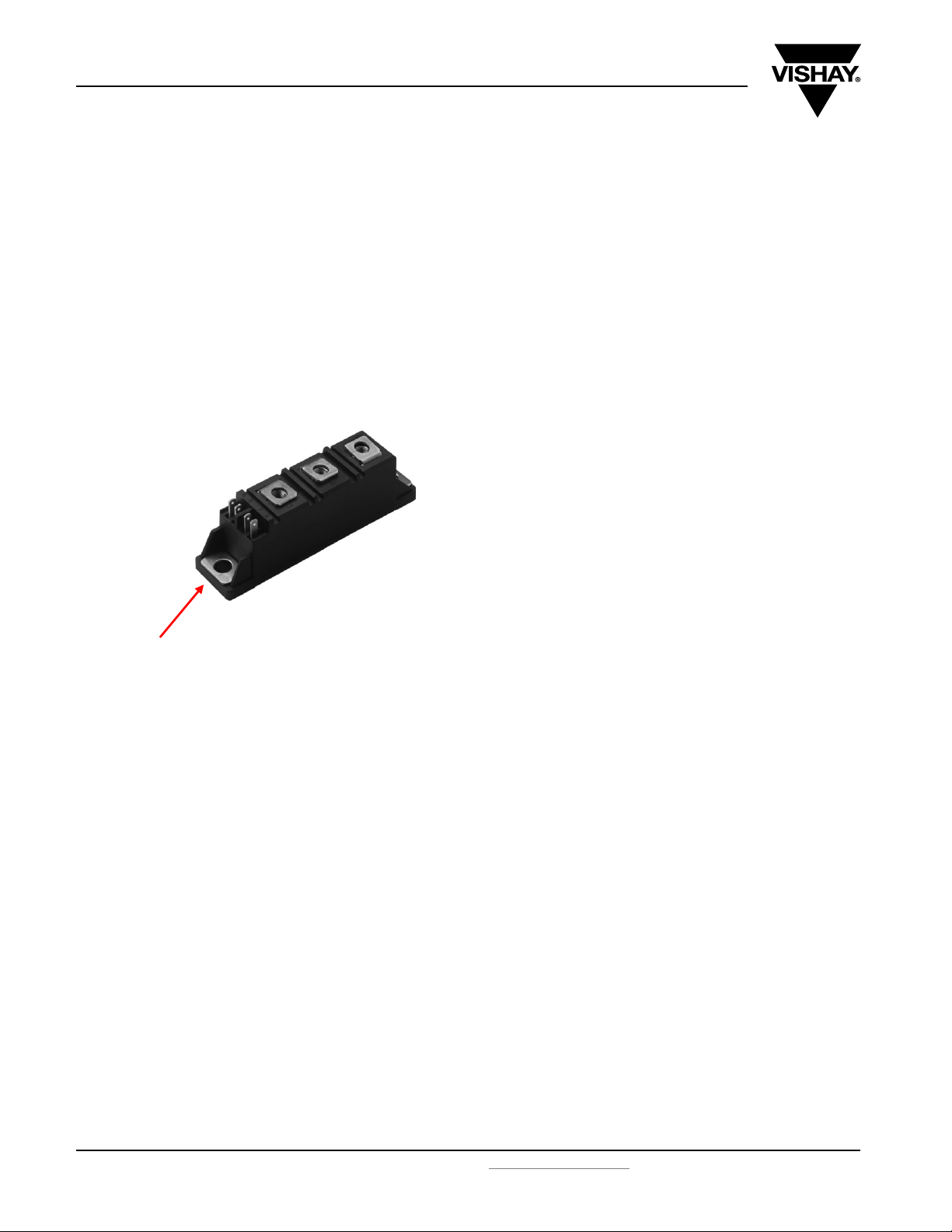
VISHAY HIGH POWER PRODUCTS
Modules
Mounting Instructions for
ADD-A-PAK Generation VII
Generation VII ADD-A-PAK (AAP) power modules combine
the excellent thermal performance enabled by a direct
bonded copper (Al2O3) substrate, superior mechanical
ruggedness, and an environmentally friendly manufacturing
process that eliminates the use of hard molds, thus reducing
direct stresses on the leads. To prevent axial pull-out, the
electrical terminals are co-molded to the module housing.
The VSK series of AAP modules uses glass passivated and
Schottky power diodes and thyristors in circuit configurations
including common anode, common cathode, half-bridge, and
single switch. The semiconductors are internally connected
through wire-bonding and electrically isolated from the
bottom baseplate, allowing the use of a common heatsink
and enabling a more compact overall assembly.
INTRODUCTION
Major AAP Generation VII module features
• High blocking voltage up to 1600 V
• Industrial standard package style, fully compatible with
TO-240AA
• High isolation capability up to V
• High surge capability with I
• No toxic material: Completely lead (Pb)-free, RoHS and UL
compliant
• Elimination of copper base plate reduces weight to 75 g
• Elimination of process steps requiring usage of chemicals
and related waste treatment promotes a cleaner and more
environmentally friendly manufacturing process
These features allow AAP Generation VII modules to fit into
existing standardized assembly processes. Important factors
in the assembly process include
• Heatsink design
• PCB, busbar, and cable design
• Power leads size/area
• Distance from adjacent heat-generating parts
The implications of these items and the requirements for
assembly of AAP Generation VII modules are discussed
over the following pages.
FSM
= 3500 V
RMS
up to 3000 A
Application Note
SPECIFYING THE HEATSINK
The heat generated by the module has to be dissipated with
a heatsink. Typically natural or forced air cooling is used.
To optimize the device performance, the contact surface of
the heatsink must be flat, with a recommended flatness of
≤ 0.03 mm (≤ 1.18 mils) and a levelling depth of less than
0.02 mm (≤ 0.79 mils), according to DIN/ISO 1302. A milled
or machined surface is generally satisfactory if prepared with
tools in good working condition. The heatsink mounting
surface must be clean, with no dirt, corrosion, or surface
oxide. It is very important to keep the mounting surface free
from particles exceeding 0.05 mm (2 mils) in thickness,
provided a thermal compound is used.
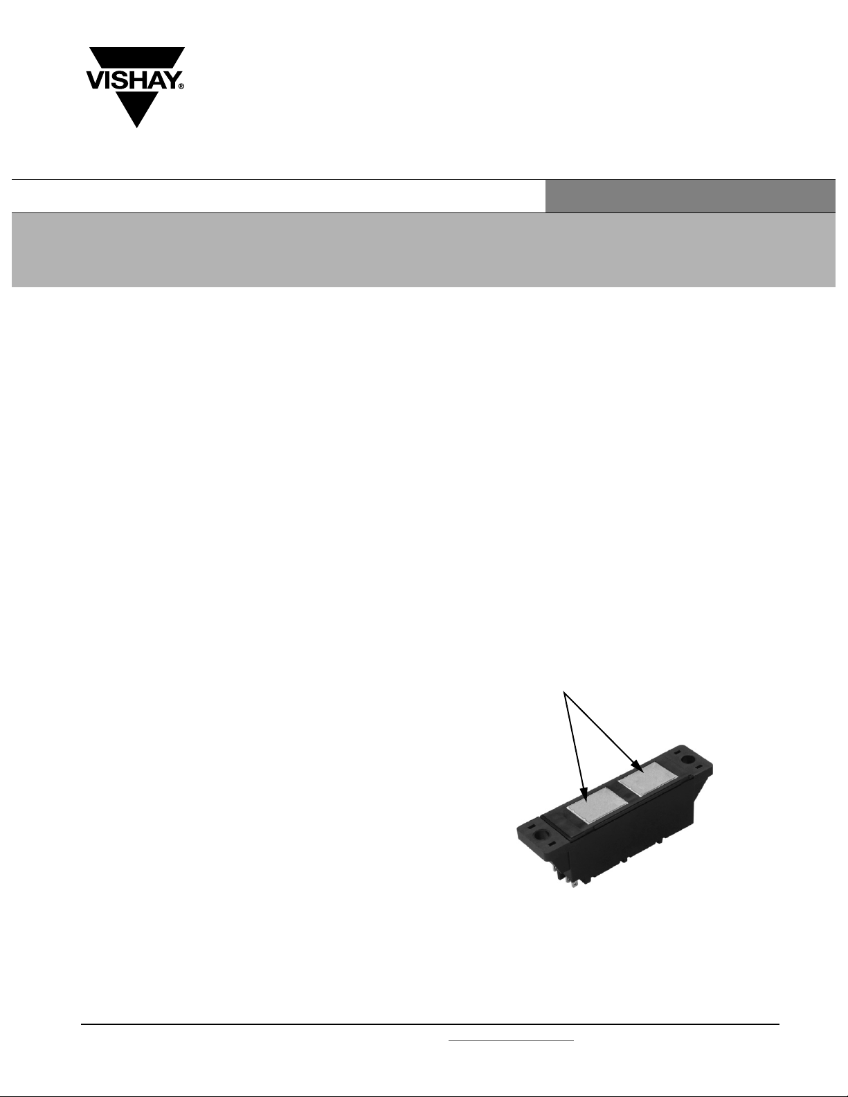
MOUNTING OPERATIONS
The AAP Generation VII modules are designed with an
exposed DBC Al2O3 substrate.
This is used to optimize the thermal behavior of the module.
To reduce the risk of damage during mounting, the ceramic
has been given additional mechanical ruggedness in the
form of two separate 15.8 mm by 21.1 mm (0.62" by 0.83")
pieces of DBC substrate, which can be seen in the photo
below.
APPLICATION NOTE
Before mounting, inspect the module to insure that the
contact surface of the bottom substrate is clean and free of
any lumps or bulges that could damage the device or impede
heat transfer across its surface.
Document Number: 95043 For technical questions, contact: ind-modules@vishay.com
Revision: 17-Dec-08 1
www.vishay.com
Page 11
Mounting Instructions for
ADD-A-PAK Generation VII
www.vishay.com For technical questions, contact: ind-modules@vishay.com
Document Number: 95043
2 Revision: 17-Dec-08
Application Note
Vishay High Power Products
APPLICATION NOTE
Next, make a uniform coating on the heatsink mounting
surfaces and module substrate with a good quality thermal
compound. Screen printing of the compound is
recommended, as well as direct application through a roller
or spatula. The datasheet values for thermal resistance
assume a uniform layer of thermal compound with a
maximum thickness of 0.08 mm. The thermal conductivity of
the compound should be no less than 0.5 W/mK. Apply
uniform pressure on the package to force the compound to
spread over the entire contact area, and check the device
bottom surface to verify full and uniform coverage.
Bolt the module to the heatsink using the two fixing holes.
An even amount of torque should be applied for each
individual mounting screw. An M6 screw should be used with
lock washers. A torque wrench, which is accurate in the
specified range, must be used in mounting the module to
achieve optimum results. The first mounting screw should be
tightened to one third of the recommended torque; the
second screw should then be tightened to the same torque.
Full tightening of both the screws can then be completed by
applying the recommended torque (see data in bulletins).
Over-tightening the mounting screw may lead to deformation
of the package, which would hence increase the thermal
resistance and damage the semiconductors. After a period of
three hours, check the torque with a final tightening in
opposite sequence to allow the spread of the compound.
Power terminals can be screwed to busbars and/or flexible
cables with eyelets.
We recommend the use of M5 screws with spring washers.
Users should consult published datasheets to determine the
optimal torque.
AAP Generation VII modules are designed to guarantee a
good and reliable contact even at 3 ± 10 % Nm on a busbar,
so there is no need to apply an especially high level of force
to obtain a good and reliable connection.
SOLDERING TO THE PCB
The signal terminal (gate and auxiliary cathode) pins of AAP
Gen VII modules based on thyristors can be soldered to the
PCB using hand iron or wave soldering processes.
The PCB should be designed with appropriate tolerances on
the hole diameters, and soldering must be done without
imposing any mechanical stress on the module pins (pulling
and tensioning the pins).
To prevent overheating of the device, the soldering time
should not exceed 8 to 10 seconds at a temperature of
260 °C.
Alternatively, a fast-on cable connector can be used to
contact the signal pins.
 Loading...