

C&H Technology VSK236PbF User Manual

6121 Baker Road,
Suite 108
Minnetonka, MN 55345
www.chtechnology.com
Phone (952) 933-6190
Fax (952) 933-6223
1-800-274-4284
Thank you for downloading this document from C&H Technology, Inc.
Please contact the C&H Technology team for the following questions -
Technical
Application
Assembly
Availability
Pricing
Phone – 1-800-274-4284
E-Mail – sales@chtechnology.com
www.chtechnology.com - SPECIALISTS IN POWER ELECTRONIC COMPONENTS AND ASSEMBLIES - www.chtechnology.com
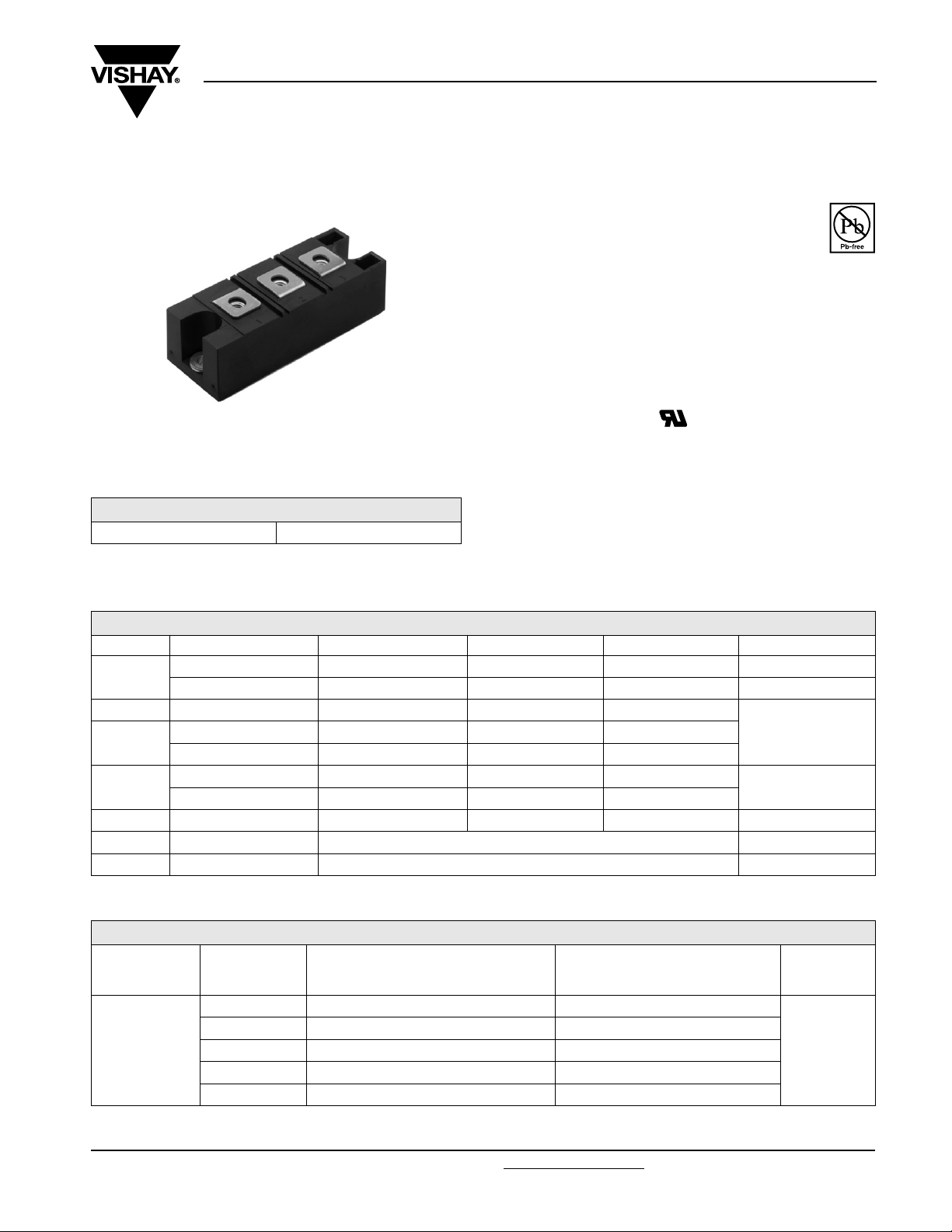
VSK.166, .196, .236..PbF Series
Vishay High Power Products
Standard Recovery Diodes, 165 A to 230 A
(New INT-A-PAK Power Modules)
FEATURES
• High voltage
• Electrically isolated by DBC ceramic (AI2O3)
New INT-A-PAK
• 3500 V
• Industrial standard package
• High surge capability
• Glass passivated chips
• Modules uses high voltage power diodes in four basic
configurations
• Simple mounting
• UL E78996 approved
• Totally lead (Pb)-free
• Designed and qualified for multiple level
isolating voltage
RMS
RoHS
COMPLIANT
PRODUCT SUMMARY
I
F(AV)
165 A to 230 A
• DC motor control and drives
• Battery chargers
•Welders
• Power converters
MAJOR RATINGS AND CHARACTERISTICS
APPLICATIONS
SYMBOL CHARACTERISTICS VSK.166.. VSK.196.. VSK.236.. UNITS
I
F(AV)
I
F(RMS)
I
FSM
2
t
I
2
√t 798 1130 1516 kA2√s
I
V
RRM
T
J
T
C
50 Hz 4000 4750 5500
60 Hz 4200 4980 5765
50 Hz 80 113 151
60 Hz 73 103 138
Range - 40 to 150 °C
165 195 230 A
100 100 100 °C
260 305 360
400 to 1600 V
ELECTRICAL SPECIFICATIONS
VOLTAGE RATINGS
V
, MAXIMUM NON-REPETITIVE
RSM
PEAK REVERSE VOLTAGE
V
TYPE NUMBER
VSK.166
VSK.196
VSK.236
V
, MAXIMUM REPETITIVE PEAK
VOLTAGE
CODE
04 400 500
08 800 900
12 1200 1300
14 1400 1500
16 1600 1700
RRM
REVERSE VOLTAGE
V
A
kA2s
I
RRM
AT 150 °C
mA
20
Document Number: 94357 For technical questions, contact: ind-modules@vishay.com
Revision: 22-Apr-08 1
www.vishay.com
VSK.166, .196, .236..PbF Series
Vishay High Power Products
Standard Recovery Diodes, 165 A to 230 A
(New INT-A-PAK Power Modules)
FORWARD CONDUCTION
PARAMETER SYMBOL TEST CONDITIONS VSK.166 VSK.196 VSK.236 UNITS
Maximum average on-state
current at case temperature
Maximum RMS on-state current I
Maximum peak, one-cycle
on-state, non-repetitive
surge current
2
Maximum I
Maximum I
t for fusing I2t
2
√t for fusing I2√t t = 0.1 to 10 ms, no voltage reapplied 798 1130 1516 kA2√s
Low level value of threshold voltage V
High level value of threshold voltage V
Low level value on-state
slope resistance
High level value on-state
Maximum forward voltage drop V
I
F(AV)
F(RMS)
I
FSM
F(TO)1
F(TO)2
r
t1
r
t2
FM
180° conduction, half sine wave
t = 10 ms
t = 8.3 ms 4200 4980 5765
t = 10 ms
t = 8.3 ms 3500 4200 4850
t = 10 ms
t = 8.3 ms 73 103 138
t = 10 ms
t = 8.3 ms 52 73 98
(16.7 % x π x I
(I > π x I
(16.7 % x π x I
(I > π x I
IFM = π x I
Average power = V
No voltage
reapplied
100 % V
RRM
reapplied
No voltage
Sine half wave,
initial T
= T
J
maximum
reapplied
100 % V
RRM
reapplied
< I < π x I
F(AV)
), TJ maximum 0.88 0.78 0.83
F(AV)
< I < π x I
F(AV)
), TJ maximum 1.26 1.2 1.07
F(AV)
, TJ = 25 °C, 180° conduction
F(AV)
F(TO)
), TJ maximum 0.73 0.69 0.7
F(AV)
), TJ maximum 1.5 1.3 1.2
F(AV)
x I
+ rf x (I
F(AV)
F(RMS)
165 195 230 A
100 100 100 °C
260 305 360
4000 4750 5500
3350 4000 4630
J
80 113 151
56 80 107
1.43 1.38 1.46 V
2
)
A
kA2s
V
mΩ
BLOCKING
PARAMETER SYMBOL TEST CONDITIONS VSK.166 VSK.196 VSK.236 UNITS
Maximum peak reverse and
off-state leakage current
RMS insulation voltage V
I
RRM
INS
TJ = 150 °C 20 mA
50 Hz, circuit to base, all terminals shorted,
t = 1 s
3500 V
THERMAL AND MECHANICAL SPECIFICATIONS
PARAMETER SYMBOL TEST CONDITIONS VSK.166 VSK.196 VSK.236 UNITS
Maximum junction operating and
storage temperature range
Maximum thermal resistance,
junction to case per junction
Maximum thermal resistance,
case to heatsink per module
Mounting
torque ± 100 %
IAP to heatsink
busbar to IAP
Approximate weight
Case style New INT-A-PAK
, T
T
J
Stg
R
thJC
DC operation 0.2 0.16 0.14
- 40 to 150 °C
K/W
R
thCS
Mounting surface smooth, flat and greased 0.05
A mounting compound is recommended and
4 to 6 Nm
the torque should be rechecked after a
period of 3 hours to allow for the spread of
the compound. Lubricated threads.
200 g
7.1 oz.
www.vishay.com For technical questions, contact: ind-modules@vishay.com
Document Number: 94357
2 Revision: 22-Apr-08
VSK.166, .196, .236..PbF Series
Standard Recovery Diodes, 165 A to 230 A
Vishay High Power Products
(New INT-A-PAK Power Modules)
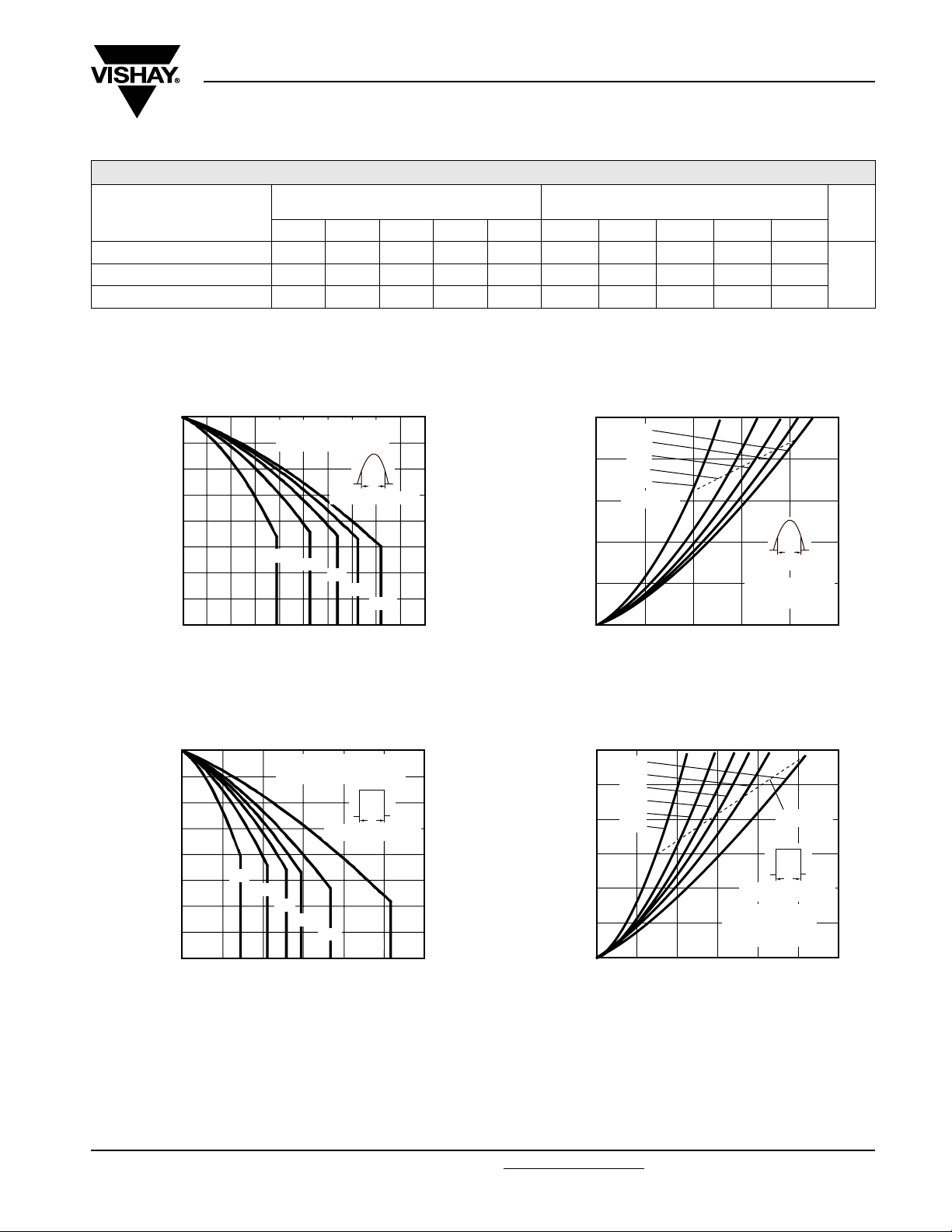
ΔR CONDUCTION PER JUNCTION
SINUSOIDAL CONDUCTION
AT T
MAXIMUM
DEVICES
J
180° 120° 90° 60° 30° 180° 120° 90° 60° 30°
VSK.166 0.025 0.03 0.038 0.055 0.089 0.018 0.031 0.041 0.057 0.089
VSK.236 0.009 0.010 0.014 0.018 0.025 0.008 0.012 0.015 0.019 0.025
Note
• Table shows the increment of thermal resistance R
150
140
130
120
110
100
Temperature (°C)
90
Maximum Allowable Case
80
70
40 80 120 160
0
VSK.166.. Series
R
(DC) = 0.20 K/W
thJC
30°
60°
Conduction angle
90°
120°
when devices operate at different conduction angles than DC
thJC
Ø
180°
200
Maximum Average Forward
Average Forward Current (A)
Fig. 1 - Current Ratings Characteristics
RECTANGULAR CONDUCTION
AT TJ MAXIMUM
250
200
150
100
Power Loss (W)
50
180°
120°
90°
60°
30°
RMS limit
Conduction angle
VSK.166.. Series
T
0
0
Average Forward Current (A)
8040 120 160
Fig. 3 - On-State Power Loss Characteristics
= 150 °C
J
UNITS
K/WVSK.196 0.016 0.019 0.024 0.034 0.053 0.012 0.02 0.026 0.035 0.054
Ø
200
150
140
130
120
110
100
Temperature (°C)
90
Maximum Allowable Case
80
70
0
30°
60°
50 100
Average Forward Current (A)
Fig. 2 - Current Ratings Characteristics
VSK.166.. Series
(DC) = 0.20 K/W
R
thJC
Ø
Conduction period
90°
120°
180°
DC
150 200 250 300
300
250
200
150
100
Power Loss (W)
50
Maximum Average Forward
0
DC
180°
120°
90°
60°
30°
0
10050 150 200
Average Forward Current (A)
Fig. 4 - On-State Power Loss Characteristics
RMS limit
Ø
Conduction period
VSK.166.. Series
Per junction
= 150 °C
T
J
250 300
Document Number: 94357 For technical questions, contact: ind-modules@vishay.com
www.vishay.com
Revision: 22-Apr-08 3
 Loading...