

Page 1

6121 Baker Road,
Suite 108
Minnetonka, MN 55345
www.chtechnology.com
Phone (952) 933-6190
Fax (952) 933-6223
1-800-274-4284
Thank you for downloading this document from C&H Technology, Inc.
Please contact the C&H Technology team for the following questions -
Technical
Application
Assembly
Availability
Pricing
Phone – 1-800-274-4284
E-Mail – sales@chtechnology.com
www.chtechnology.com - SPECIALISTS IN POWER ELECTRONIC COMPONENTS AND ASSEMBLIES - www.chtechnology.com
Page 2
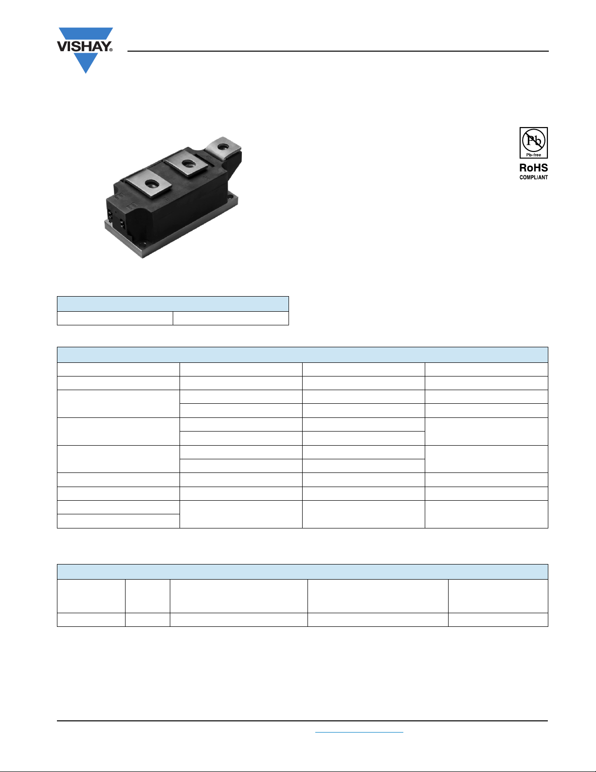
Thyristor/Diode, 500 A
(SUPER MAGN-A-PAK
VSHPS1480
Vishay High Power Products
TM
Power Modules)
FEATURES
• High current capability
• High surge capability
• Industrial standard package
• 3000 V
• Compliant to RoHS directive 2002/95/EC
• Designed and qualified for industrial level
isolating voltage with non-toxic substrate
RMS
SUPER MAGN-A-PAK
TM
TYPICAL APPLICATIONS
• Motor starters
PRODUCT SUMMARY
I
or I
T(AV)
F(AV)
500 A
• DC motor controls - AC motor controls
• Uninterruptable power supplies
MAJOR RATINGS AND CHARACTERISTICS
SYMBOL CHARACTERISTICS VALUES UNITS
I
or I
T(AV)
F(AV)
I
T(RMS)
I
TSM
2
t
I
2
I
√t 15 910 kA2√s
V
RRM/VDRM
T
Stg
T
J
82 °C 500 A
785 A
T
C
50 Hz 17 800
60 Hz 18 700
50 Hz 1591
60 Hz 1452
Range - 40 to 130 °C
82
kA2s
1800 V
°C
A
ELECTRICAL SPECIFICATIONS
VOLTAGE RATINGS
V
TYPE NUMBER
VSHPS1480 18 1800 1900 100
Document Number: 00266x For technical questions, contact: ind-modules@vishay.com
Revision: 05-May-09 1
VOLTAGE
CODE
RRM/VDRM
, MAXIMUM REPETITIVE
PEAK REVERSE VOLTAGE
V
V
, MAXIMUM NON-REPETITIVE
RSM
PEAK REVERSE VOLTAGE
V
I
RRM/IDRM
AT T
MAXIMUM
= 125 °C
J
mA
www.vishay.com
Page 3

VSHPS1480
Vishay High Power Products
Thyristor/Diode, 500 A
(SUPER MAGN-A-PAKTM Power Modules)
ON-STATE CONDUCTION
PARAMETER SYMBOL TEST CONDITIONS VALUES UNITS
Maximum average on-state current
at case temperature
Maximum RMS on-state current I
Maximum peak, one-cycle,
I
I
T(RMS)
I
non-repetitive on-state surge current
2
Maximum I
Maximum I
t for fusing I2t
2
√t for fusing I2√t t = 0.1 ms to 10 ms, no voltage reapplied 15 910 kA2√s
Low level value or threshold voltage V
High level value of threshold voltage V
Low level value on-state slope resistance r
High level value on-state slope resistance r
Maximum peak on-state or
forward voltage
Maximum holding current I
Maximum latching current I
T(AV),
F(AV)
180° conduction, half sine wave
180° conduction, half sine wave at TC = 82 °C 785 A
t = 10 ms
TSM,
I
FSM
t = 8.3 ms 18.7
t = 10 ms
t = 8.3 ms 15.7
t = 10 ms
t = 8.3 ms 1452
t = 10 ms
t = 8.3 ms 1027
T(TO)1
T(TO)2
V
V
(16.7 % x π x I
(I > π x I
(16.7 % x π x I
t1
(I > π x I
t2
TM
Ipk = 1500 A, TJ = 25 °C, tp = 10 ms sine pulse 1.50 V
FM
H
TJ = 25 °C, anode supply 12 V resistive load
L
No voltage
reapplied
100 % V
reapplied
RRM
Sinusoidal
half wave,
No voltage
reapplied
100 % V
RRM
initial T
= TJ maximum
J
reapplied
< I < π x I
T(AV)
), TJ = TJ maximum 0.93
T(AV)
< I < π x I
T(AV)
), TJ = TJ maximum 0.32
T(AV)
), TJ = TJ maximum 0.85
T(AV)
), TJ = TJ maximum 0.36
T(AV)
500 A
82 °C
17.8
15.0
1591
1125
500
1000
kA
kA2s
V
mΩ
mA
SWITCHING
PARAMETER SYMBOL TEST CONDITIONS VALUES UNITS
Maximum rate of rise of turned-on current dI/dt T
Typical delay time t
Typical turn-off time t
d
q
= TJ maximum, ITM = 400 A, V
J
Gate current 1 A, dIg/dt = 1 A/µs
V
= 0.67 % V
d
I
= 750 A; TJ = TJ maximum, dI/dt = - 60 A/µs,
TM
V
= 50 V, dV/dt = 20 V/µs, gate 0 V 100 Ω
R
, TJ = 25 °C
DRM
applied 1000 A/µs
DRM
2.0
200
µs
BLOCKING
PARAMETER SYMBOL TEST CONDITIONS VALUES UNITS
Maximum critical rate of rise
of off-state voltage
RMS insulation voltage V
Maximum peak reverse and
off-state leakage current
dV/dt T
INS
I
RRM
I
DRM
www.vishay.com For technical questions, contact: ind-modules@vishay.com
2 Revision: 05-May-09
= 130 °C, linear to VD = 80 % V
J
DRM
1000 V/µs
t = 1 s 3000 V
,
TJ = 125 °C, rated V
DRM/VRRM
applied 100 mA
Document Number: 00266x
Page 4

VSHPS1480
Thyristor/Diode, 500 A
Vishay High Power Products
(SUPER MAGN-A-PAKTM Power Modules)
TRIGGERING
PARAMETER SYMBOL TEST CONDITIONS VALUES UNITS
Maximum peak gate power P
Maximum peak average gate power P
Maximum peak positive gate current +I
Maximum peak positive gate voltage +V
Maximum peak negative gate voltage -V
Maximum DC gate current required to trigger I
DC gate voltage required to trigger V
DC gate current not to trigger I
DC gate voltage not to trigger V
GM
G(AV)
GM
GM
GM
GT
GT
GD
GD
THERMAL AND MECHANICAL SPECIFICATIONS
PARAMETER SYMBOL TEST CONDITIONS VALUES UNITS
Maximum junction operating
temperature range
Maximum storage temperature range T
Maximum thermal resistance,
junction to case per junction
Maximum thermal resistance,
case to heatsink
SMAP to heatsink
Mounting torque ± 10 %
busbar to SMAP 12-15
R
R
T
J
Stg
thJC
thC-hs
TJ = TJ maximum, tp ≤ 5 ms 10
TJ = TJ maximum, f = 50 Hz, d% = 50 2.0
3.0 A
TJ = TJ maximum, tp ≤ 5 ms
TJ = 25 °C, Vak 12 V
TJ = TJ maximum 10 mA
DC operation 0.065
A mounting compound is recommended and the
torque should be rechecked after a period of
3 hours to allow for the spread of the compound.
20
5.0
200 mA
3.0 V
0.25 V
- 40 to 130
- 40 to 150
0.02
6-8
W
°C
K/W
Nm
V
Approximate weight 1500 g
Case style See dimensions SUPER MAGN-A-PAK
ΔR
CONDUCTION ANGLE SINUSOIDAL CONDUCTION RECTANGULAR CONDUCTION TEST CONDITIONS UNITS
Note
• Table shows the increment of thermal resistance R
Document Number: 00266x For technical questions, contact: ind-modules@vishay.com
Revision: 05-May-09 3
CONDUCTION
thJC
180° 0.009 0.006
120° 0.011 0.011
90° 0.014 0.015
60° 0.021 0.022
30° 0.037 0.038
when devices operate at different conduction angles than DC
thJC
T
= TJ maximum K/W
J
www.vishay.com
Page 5

VSHPS1480
Vishay High Power Products
CIRCUIT CONFIGURATION
DIMENSIONS in millimeters (inches)
Thyristor/Diode, 500 A
(SUPER MAGN-A-PAKTM Power Modules)
1
~
+
2
-
3
4 (K1)
5 (G1)
60.0 (2.36)
48.0 (1.89)
1.0 (0.039)
31.0
(1.22)
26.0
(0.98)
50.0
(1.97)
M10
32
26.0
(0.98)
112.0 (4.41)
124.0 (4.88)
149.0 (5.67)
44.0
(1.73)
52 (2.05)
Fast-on tabs
2.8 x 0.8 (0.11 x 0.03)
54
1
28.0
(1.10)
20.1
6
7
36.4 (1.14) 4.5 (0.20)
5, 6 = Gate
4, 7 = Cathode
(0.78)
www.vishay.com For technical questions, contact: ind-modules@vishay.com
Document Number: 00266x
4 Revision: 05-May-09
 Loading...