


6121 Baker Road,
Suite 108
Minnetonka, MN 55345
www.chtechnology.com
Phone (952) 933-6190
Fax (952) 933-6223
1-800-274-4284
Thank you for downloading this document from C&H Technology, Inc.
Please contact the C&H Technology team for the following questions -
Technical
Application
Assembly
Availability
Pricing
Phone – 1-800-274-4284
E-Mail – sales@chtechnology.com
www.chtechnology.com - SPECIALISTS IN POWER ELECTRONIC COMPONENTS AND ASSEMBLIES - www.chtechnology.com
www.vishay.com
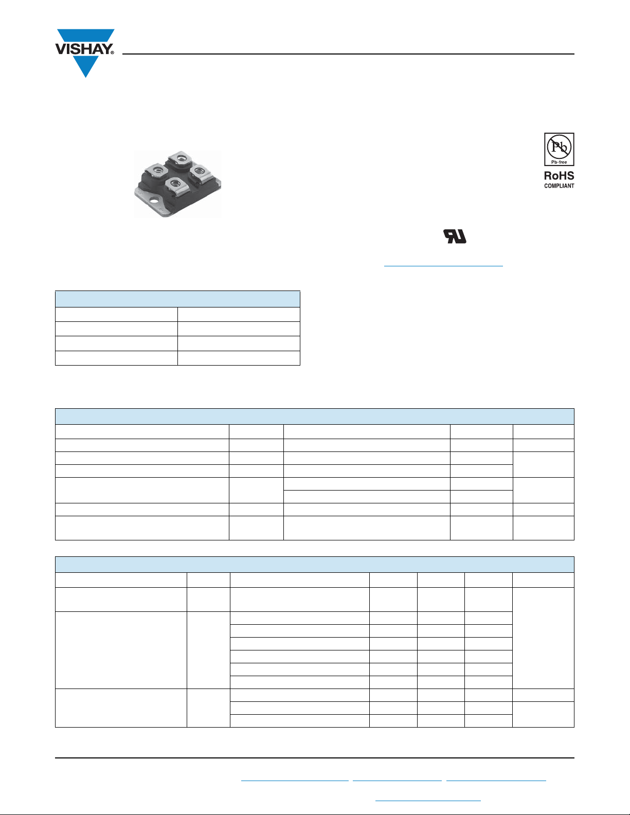
SOT-227
Ultrafast Soft Recovery Diode, 70 A
PRODUCT SUMMARY
V
R
(typical) 2.2 V
V
F
t
(typical) 48 ns
rr
I
at TC, per module 70 A at 121 °C
F(DC)
1200 V
HEXFRED®
FEATURES
• Fast recovery time characteristic
• Electrically isolated base plate
• Antiparallel diodes
• Large creepage distance between terminal
• Simplified mechanical designs, rapid assembly
• Designed and qualified for industrial level
• UL approved file E78996
• Material categorization: For definitions of compliance
please see www.vishay.com/doc?99912
DESCRIPTION/APPLICATIONS
This SOT-227 modules with HEXFRED® rectifier are in
antiparallel configuration. The antiparallel configuration is
used for simple series rectifier and high voltage application.
The semiconductor in the SOT-227 package is isolated from
the copper base plate, allowing for common heatsinks and
compact assemblies to be built.
These modules are intended for general applications such
as HV power supplies, electronic welders, motor control and
inverters.
VS-HFA70EA120
Vishay Semiconductors
ABSOLUTE MAXIMUM RATINGS
PARAMETER SYMBOL TEST CONDITIONS MAX. UNITS
Cathode to anode voltage V
Continuous forward current, per leg I
Single pulse forward current I
Maximum power dissipation, per leg P
RMS isolation voltage V
Operating junction and storage
temperature range
T
J
FSM
ISOL
, T
R
F
D
TC = 121 °C 35
TJ = 25 °C 350
TC = 25 °C 357
= 100 °C 143
T
C
Any terminal to case, t = 1 minute 2500 V
Stg
1200 V
A
W
- 55 to + 150 °C
ELECTRICAL SPECIFICATIONS (TJ = 25 °C unless otherwise specified)
PARAMETER SYMBOL TEST CONDITIONS MIN. TYP. MAX. UNITS
Cathode to anode
breakdown voltage
Forward voltage, per leg V
Reverse leakage current, per leg I
V
RM
IR = 100 μA 1200 - -
BR
IF = 30 A - 2.2 3.0
= 60 A - 2.8 4.0
I
F
I
= 30 A, TJ = 125 °C - 2.13 -
FM
F
I
= 60 A, TJ = 125 °C - 2.70 -
F
I
= 30 A, TJ = 150 °C - 2.04 -
F
I
= 60 A, TJ = 150 °C - 2.65 -
F
VR = VR rated - 2.0 75 μA
T
= 125 °C, VR = VR rated - 1.6 5
J
= 150 °C, VR = VR rated - 5 10
T
J
V
mA
Revision: 20-Jul-12
1
For technical questions within your region: DiodesAmericas@vishay.com
THIS DOCUMENT IS SUBJECT TO CHANGE WITHOUT NOTICE. THE PRODUCTS DESCRIBED HEREIN AND THIS DOCUMENT
ARE SUBJECT TO SPECIFIC DISCLAIMERS, SET FORTH AT www.vishay.com/doc?91000
, DiodesAsia@vishay.com, DiodesEurope@vishay.com
Document Number: 94747
VS-HFA70EA120
www.vishay.com
DYNAMIC RECOVERY CHARACTERISTICS (TJ = 25 °C unless otherwise specified)
PARAMETER SYMBOL TEST CONDITIONS MIN. TYP. MAX. UNITS
IF = 1 A; dIF/dt = 200 A/μs; VR = 30 V - 48 -
Reverse recovery time, per leg t
Peak recovery current, per leg I
Reverse recovery charge, per leg Q
Junction capacitance, per leg C
rr
RRM
rr
T
= 25 °C
J
T
= 125 °C - 218 -
J
TJ = 25 °C - 13 -
T
= 125 °C - 19 -
J
TJ = 25 °C - 910 -
T
= 125 °C - 1920 -
J
I
= 50 A
F
/dt = - 200 A/μs
dI
F
= 200 V
V
R
VR = 1200 V - 27 - pF
THERMAL - MECHANICAL SPECIFICATIONS
PARAMETER SYMBOL TEST CONDITIONS MIN. TYP. MAX. UNITS
Junction to case, single leg conducting
Case to heatsink, per leg R
Weight -30- g
Mounting torque, on terminals and heatsink T - - 1.3 Nm
R
thJC
thCS
Flat, greased and surface - 0.05 -
Vishay Semiconductors
- 145 -
--0.35
nsT
A
nC
°C/WJunction to case, both legs conducting - - 0.175
Revision: 20-Jul-12
For technical questions within your region: DiodesAmericas@vishay.com
2
, DiodesAsia@vishay.com, DiodesEurope@vishay.com
Document Number: 94747
THIS DOCUMENT IS SUBJECT TO CHANGE WITHOUT NOTICE. THE PRODUCTS DESCRIBED HEREIN AND THIS DOCUMENT
ARE SUBJECT TO SPECIFIC DISCLAIMERS, SET FORTH AT www.vishay.com/doc?91000

www.vishay.com
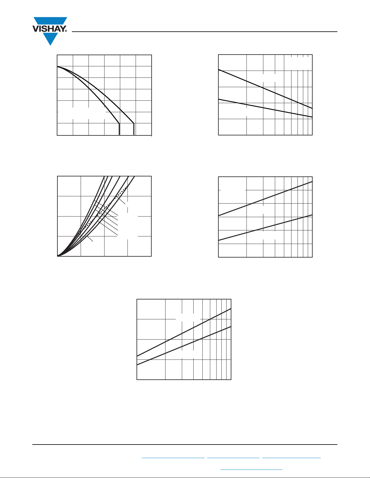
0.01
0.1
1
0.0001 0.001
0.01
0.1 1
10
t1 - Rectangular Pulse Duration (s)
Z
thJC
- Thermal Impedance (°C/W)
D = 0.75
D = 0.50
D = 0.33
D = 0.25
D = 0.20
P
DM
t
2
t
1
Notes:
1. Duty factor D = t
1/t2
2. Peak TJ = PDM x Z
thJC
+ T
C
DC
VS-HFA70EA120
Vishay Semiconductors
1000
100
10
1
- Instantaneous Forward Current (A)
F
I
0.5 1.5 2.5 3.5 5.01.0 2.0 3.0 4.0 4.5
TJ = 150 °C
= 125 °C
T
J
T
= 25 °C
J
VFM - Forward Voltage Drop (V)
10 000
1000
- Reverse Current (µA)
R
I
TJ = 150 °C
100
10
1
0.1
0.01
2000 400 600 800 1000 1200
VR - Reverse Voltage (V)
TJ = 125 °C
TJ = 25 °C
Fig. 1 - Typical Forward Voltage Drop Characteristics Fig. 2 - Typical Values of Reverse Current vs.
Reverse Voltage
1000
100
Revision: 20-Jul-12
For technical questions within your region: DiodesAmericas@vishay.com
THIS DOCUMENT IS SUBJECT TO CHANGE WITHOUT NOTICE. THE PRODUCTS DESCRIBED HEREIN AND THIS DOCUMENT
- Junction Capacitance (pF)
T
C
Fig. 3 - Typical Junction Capacitance vs. Reverse Voltage
Fig. 4 - Maximum Thermal Impedance Z
ARE SUBJECT TO SPECIFIC DISCLAIMERS, SET FORTH AT www.vishay.com/doc?91000
10
10
VR - Reverse Voltage (V)
100
1000
3
thJC
, DiodesAsia@vishay.com, DiodesEurope@vishay.com
10 000
Characteristics
Document Number: 94747
www.vishay.com
Allowable Case Temperature (°C)
I
F(AV)
- Average Forward Current (A)
604020 80
100 120
0
0
50
75
25
100
150
175
125
Square wave (D = 0.50)
80 % rated V
R
applied
DC
t
rr
(ns)
dIF/dt (A/µs)
100 1000
50
300
250
100
150
200
IF = 50 A
V
R
= 200 V
TJ = 25 °C
TJ = 125 °C
Q
rr
(nC)
dIF/dt (A/µs)
100 1000
0
3000
2500
1000
1500
2000
500
IF = 50 A
V
R
= 200 V
TJ = 25 °C
TJ = 125 °C
VS-HFA70EA120
Vishay Semiconductors
Fig. 5 - Maximum Allowable Case Temperature vs.
Average Forward Current
200
150
RMS limit
100
50
Average Power Loss (W)
0
I
- Average Forward Current (A)
F(AV)
DC
D = 0.20
D = 0.25
D = 0.33
D = 0.50
D = 0.75
Fig. 6 - Forward Power Loss Characteristics
40
30
806040200
IF = 50 A
= 200 V
V
R
TJ = 125 °C
Fig. 7 - Typical Reverse Recovery Time vs. dIF/dt
Fig. 8 - Typical Stored Charge vs. dI
/dt
F
Note
(1)
Revision: 20-Jul-12
Formula used: TC = TJ - (Pd + Pd
Pd = Forward power loss = I
Pd
= Inverse power loss = VR1 x IR (1 - D); IR at VR1 = Rated V
REV
For technical questions within your region: DiodesAmericas@vishay.com
THIS DOCUMENT IS SUBJECT TO CHANGE WITHOUT NOTICE. THE PRODUCTS DESCRIBED HEREIN AND THIS DOCUMENT
20
(A)
rr
I
TJ = 25 °C
dIF/dt (A/µs)
R
/dt
F
F(AV)
) x R
REV
x VFM at (I
10
0
100 1000
Fig. 9 - Typical Peak Recovery Current vs. dI
;
thJC
/D) (see fig. 5);
F(AV)
4
, DiodesAsia@vishay.com, DiodesEurope@vishay.com
ARE SUBJECT TO SPECIFIC DISCLAIMERS, SET FORTH AT www.vishay.com/doc?91000
Document Number: 94747

www.vishay.com
Q
rr
0.5 I
RRM
dI
(rec)M
/dt
0.75 I
RRM
I
RRM
t
rr
t
b
t
a
I
F
dIF/dt
0
(1)
(2)
(3)
(4)
(5)
(1) dI
F
/dt - rate of change of current
through zero crossing
(2) I
RRM
- peak reverse recovery current
(3) t
rr
- reverse recovery time measured
from zero crossing point of negative
going I
F
to point where a line passing
through 0.75 I
RRM
and 0.50 I
RRM
extrapolated to zero current.
(4) Q
rr
- area under curve dened by t
rr
and I
RRM
trr x I
RRM
2
Q
rr
=
(5) dI
(rec)M
/dt - peak rate of change of
current during t
b
portion of t
rr
L = 70 μH
= 200 V
V
R
VS-HFA70EA120
Vishay Semiconductors
0.01 Ω
D.U.T.
dIF/dt
adjust
G
D
IRFP250
S
Fig. 10 - Reverse Recovery Parameter Test Circuit
Revision: 20-Jul-12
For technical questions within your region: DiodesAmericas@vishay.com
THIS DOCUMENT IS SUBJECT TO CHANGE WITHOUT NOTICE. THE PRODUCTS DESCRIBED HEREIN AND THIS DOCUMENT
Fig. 11 - Reverse Recovery Waveform and Definitions
ARE SUBJECT TO SPECIFIC DISCLAIMERS, SET FORTH AT www.vishay.com/doc?91000
5
, DiodesAsia@vishay.com, DiodesEurope@vishay.com
Document Number: 94747
www.vishay.com
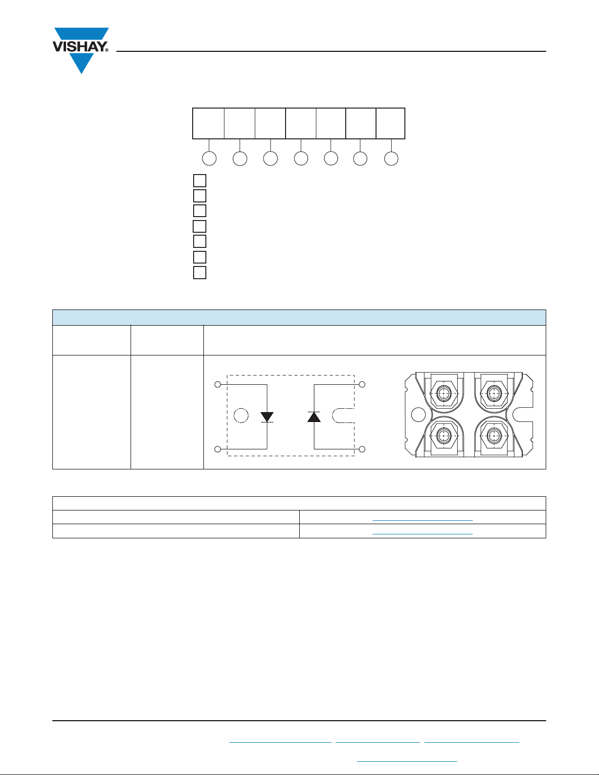
1
43
2
Lead Assignment
4
12
3
ORDERING INFORMATION TABLE
VS-HFA70EA120
Vishay Semiconductors
Device code
CIRCUIT CONFIGURATION
CIRCUIT
CIRCUIT
CONFIGURATION
CODE
HFVS- A 70 E A 120
1
1
- Vishay Semiconductors product
2
- HEXFRED® family
3
- Process designator (A = Electron irradiated)
4
- Average current (70 = 70 A)
5
- Circuit configuration (2 separate diodes, antiparallel pin-out)
- Package indicator (SOT-227 standard isolated base)
6
- Voltage rating (120 = 1200 V)
7
32 4 6 7
5
CIRCUIT DRAWING
2 separate diodes,
antiparallel pin-out
Dimensions www.vishay.com/doc?95423
Part marking information www.vishay.com/doc?95425
E
LINKS TO RELATED DOCUMENTS
Revision: 20-Jul-12
For technical questions within your region: DiodesAmericas@vishay.com
THIS DOCUMENT IS SUBJECT TO CHANGE WITHOUT NOTICE. THE PRODUCTS DESCRIBED HEREIN AND THIS DOCUMENT
6
ARE SUBJECT TO SPECIFIC DISCLAIMERS, SET FORTH AT www.vishay.com/doc?91000
Document Number: 94747
, DiodesAsia@vishay.com, DiodesEurope@vishay.com

Legal Disclaimer Notice
www.vishay.com
Vishay
Disclaimer
ALL PRODUCT, PRODUCT SPECIFICATIONS AND DATA ARE SUBJECT TO CHANGE WITHOUT NOTICE TO IMPROVE
RELIABILITY, FUNCTION OR DESIGN OR OTHERWISE.
Vishay Intertechnology, Inc., its affiliates, agents, and employees, and all persons acting on its or their behalf (collectively,
“Vishay”), disclaim any and all liability for any errors, inaccuracies or incompleteness contained in any datasheet or in any other
disclosure relating to any product.
Vishay makes no warranty, representation or guarantee regarding the suitability of the products for any particular purpose or
the continuing production of any product. To the maximum extent permitted by applicable law, Vishay disclaims (i) any and all
liability arising out of the application or use of any product, (ii) any and all liability, including without limitation special,
consequential or incidental damages, and (iii) any and all implied warranties, including warranties of fitness for particular
purpose, non-infringement and merchantability.
Statements regarding the suitability of products for certain types of applications are based on Vishay’s knowledge of typical
requirements that are often placed on Vishay products in generic applications. Such statements are not binding statements
about the suitability of products for a particular application. It is the customer’s responsibility to validate that a particular
product with the properties described in the product specification is suitable for use in a particular application. Parameters
provided in datasheets and/or specifications may vary in different applications and performance may vary over time. All
operating parameters, including typical parameters, must be validated for each customer application by the customer’s
technical experts. Product specifications do not expand or otherwise modify Vishay’s terms and conditions of purchase,
including but not limited to the warranty expressed therein.
Except as expressly indicated in writing, Vishay products are not designed for use in medical, life-saving, or life-sustaining
applications or for any other application in which the failure of the Vishay product could result in personal injury or death.
Customers using or selling Vishay products not expressly indicated for use in such applications do so at their own risk and agree
to fully indemnify and hold Vishay and its distributors harmless from and against any and all claims, liabilities, expenses and
damages arising or resulting in connection with such use or sale, including attorneys fees, even if such claim alleges that Vishay
or its distributor was negligent regarding the design or manufacture of the part. Please contact authorized Vishay personnel to
obtain written terms and conditions regarding products designed for such applications.
No license, express or implied, by estoppel or otherwise, to any intellectual property rights is granted by this document or by
any conduct of Vishay. Product names and markings noted herein may be trademarks of their respective owners.
Material Category Policy
Vishay Intertechnology, Inc. hereby certifies that all its products that are identified as RoHS-Compliant fulfill the
definitions and restrictions defined under Directive 2011/65/EU of The European Parliament and of the Council
of June 8, 2011 on the restriction of the use of certain hazardous substances in electrical and electronic equipment
(EEE) - recast, unless otherwise specified as non-compliant.
Please note that some Vishay documentation may still make reference to RoHS Directive 2002/95/EC. We confirm that
all the products identified as being compliant to Directive 2002/95/EC conform to Directive 2011/65/EU.
Revision: 12-Mar-12
1
Document Number: 91000
 Loading...