

Page 1

6121 Baker Road,
Suite 108
Minnetonka, MN 55345
Phone (952) 933-6190
Fax (952) 933-6223
(800) 274-4284
Thank you for downloading this document from C&H Technology, Inc.
Please contact the C&H Technology team for the following questions -
Technical
Application
Assembly
Availability
Pricing
Phone – 1-800-274-4284
E-Mail – sales@chtechnology.com
C & H TECHNOLOGY, INC. ● 6121 BAKER RD. SUITE 108 ● MINNETONKA, MINNESOTA 55345 ●
800-274-4284 ● 952-933-6190 ● FAX: 952-933-6223 ● WWW.CHTECHNOLOGY.COM
Page 2
www.vishay.com
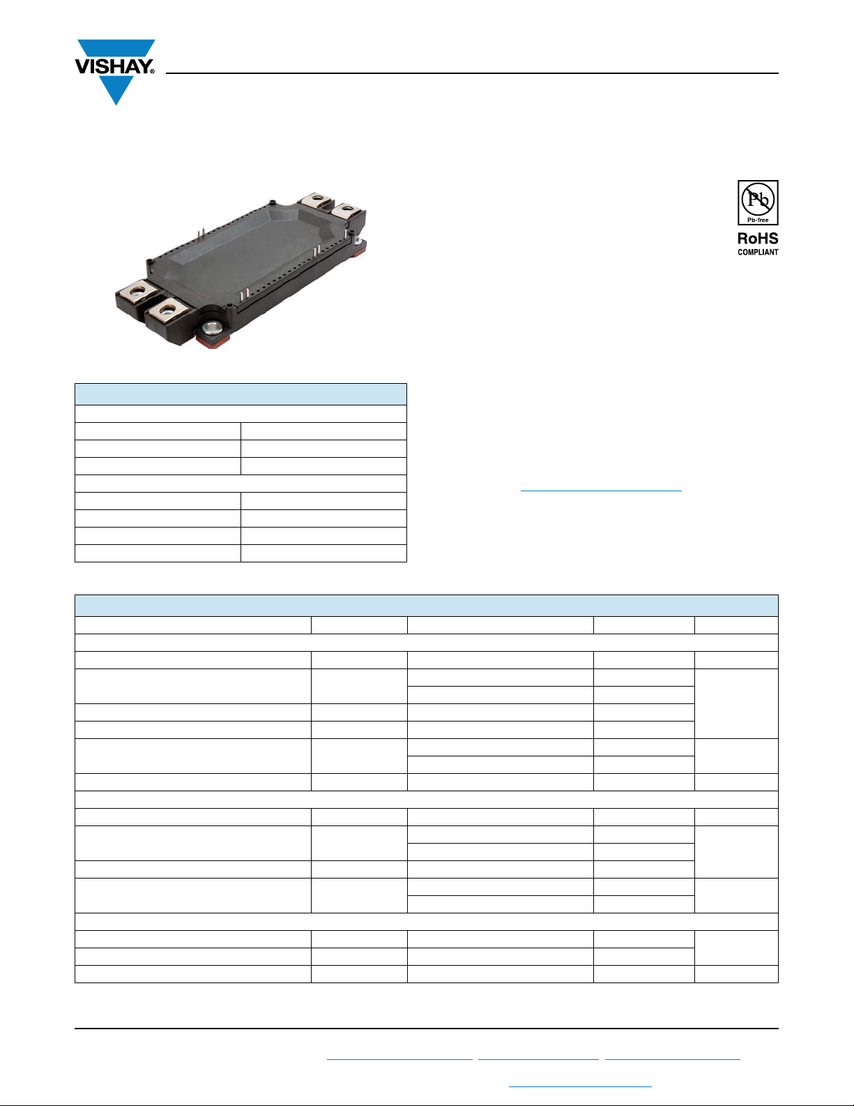
X-MAP
Half-Bridge - Trench IGBT, 450 A
PRODUCT SUMMARY
IGBT
V
CES
V
(typical) at 450 A, 25 °C 2.49 V
CE(on)
I
at 87 °C 450 A
D(DC)
HEXFRED
trr (typical) 370 ns
I
at 25 °C 412 A
F(DC)
Type Modules - IGBT
Package X-MAP
®
Preliminary
X-MAP Power Module
FEATURES AND BENEFITS
• Trench IGBT technology with positive
temperature coefficient
• Square RBSOA
• 10 μs short circuit capability
• HEXFRED antiparallel diodes with soft reverse recovery
•T
maximum = 175 °C
J
• Fully isolated package
• Industry standard outline
• Designed for increased operating efficiency in power
conversion: UPS, SMPS, welding, induction heating
• Easy to assemble and parallel
• Direct mounting to heatsink
1200 V
• Speed 4 kHz to 30 kHz
• Very low V
CE(on)
• Material categorization: For definitions of compliance
please see www.vishay.com/doc?99912
REMARKS
• Product reliability results valid for TJ = 150 °C
• Recommended operation temperature T
VS-GT450TX120U
Vishay Semiconductors
= 150 °C
op
ABSOLUTE MAXIMUM RATINGS
PARAMETER SYMBOL TEST CONDITIONS MAX. UNITS
IGBT
Collector to emitter voltage V
Continuous collector current, V
Pulsed collector current I
Clamped inductive load current I
Power dissipation P
Gate to source voltage V
HEXFRED
Peak repetitive reverse voltage V
Continuous forward current I
Peak repetitive forward current I
Power dissipation P
MODULE
Operating junction temperature range T
Storage temperature range T
RMS isolation voltage V
Note
(1)
Maximum I
Revision: 23-Jul-13
For technical questions within your region: DiodesAmericas@vishay.com
THIS DOCUMENT IS SUBJECT TO CHANGE WITHOUT NOTICE. THE PRODUCTS DESCRIBED HEREIN AND THIS DOCUMENT
current admitted 600 A to do not exceed the maximum temperature of terminals.
RMS
ARE SUBJECT TO SPECIFIC DISCLAIMERS, SET FORTH AT www.vishay.com/doc?91000
at 15 V I
GE
CES
C
CM
LM
GE
RRM
F
FSM
Stg
ISOL
TC = 25 °C
T
= 80 °C 473
C
D
D
J
TC = 25 °C 2500
= 80 °C 1583
T
C
TC = 25 °C 412
= 80 °C 308
C
TC = 25 °C 1250
= 80 °C 792
T
C
Any terminal to case, t = 1 s 3500 V
1
(1)
, DiodesAsia@vishay.com, DiodesEurope@vishay.com
1200 V
628
n/a
n/a
± 30 V
1200 V
n/a
- 55 to + 175
- 40 to + 175
Document Number: 93615
A
W
AT
W
°C
Page 3
Preliminary
VS-GT450TX120U
www.vishay.com
ELECTRICAL SPECIFICATIONS (TJ = 25 °C unless otherwise specified)
PARAMETER SYMBOL TEST CONDITIONS MIN. TYP. MAX. UNITS
Collector to emitter breakdown voltage V
Breakdown voltage
temperature coefficient
V
BR(CES)
(BR)CES
Collector to emitter voltage V
Gate threshold voltage V
Forward transconductance g
Collector to emitter leakage current I
Gate to emitter leakage current I
Total gate charge (turn-on) Q
Gate to collector charge (turn-on) Q
Turn-on switching loss E
Turn-off switching loss E
Turn-on switching loss E
Turn-off switching loss E
Turn-on delay time t
Rise time t
Turn-off delay time t
Fall time t
Input capacitance C
Reverse transfer capacitance C
Forward voltage V
Reverse recovery time t
Reverse recovery charge Q
Junction capacitance C
CE(on)
GE(th)
fe
CES
GES
g
ge
gc
on
off
on
off
d(on)
r
d(off)
f
iss
oss
rss
F
rr
rr
T
VGE = 0 V, IC = 500 μA 1200 - - V
/TJReference to 25 °C, IC = 1 mA - n/a - V/°C
VGE = 15 V, IC = 450 A - 2.49 -
= 15 V, IC = 450 A, TJ = 125 °C - 2.84 -
V
GE
VCE = VGE, IC = 1.0 mA - 4.9 - V
VCE = 20 V, IC = 450 A - 525 - S
VGE = 0 V, VCE= 1200 V - 0.07 -
= 0 V, VCE= 1200 V, TJ = 125 °C - 4 -
V
GE
VGE = ± 30 V - - ± 400 nA
IC = 450 A
V
= 600 V
CE
V
= 15 V
GE
IC = 450 A, VCC = 600 V, VGE = 15 V,
R
= 3.3 , L = 500 μH, TJ = 25 °C
g
VCC = 600 V, TJ = 125 °C
I
= 450 A
C
R
= 3.3 , L = 500 μH
g
= 15 V
V
GS
VGE = 0 V
V
= 30 V
CE
f = 1.0 MHz
IF = 450 A - 2.68 -
= 450 A, TJ = 125 °C - 3.0 -
I
F
IF = 450 A, L = 500 μH, Rg = 3.3 ,
V
= 600 V
R
= 450 A, L = 500 μH, Rg = 3.3 ,
I
F
= 600 V, TJ = 125 °C
V
R
IF = 450 A, L = 500 μH, Rg = 3.3 ,
V
= 600 V
R
= 450 A, L = 500 μH, Rg = 3.3 ,
I
F
V
= 600 V, TJ = 125 °C
R
VR = 1200 V - n/a - pF
Vishay Semiconductors
V
mA
-2490-
-540-
-1140-
- 51.8 -
- 33.0 -
- 62.4 -
-50-
-830-
-249-
-862-
-134-
- 53.7 -
-2-
-1.5-
-370-
-511-
- 15.8 -
- 39.8 -
nCGate to emitter charge (turn-on) Q
mJ
ns
nFOutput capacitance C
V
ns
μC
INTERNAL NTC - THERMISTOR SPECIFICATIONS
PARAMETER SYMBOL TEST CONDITIONS TYP. UNITS
Resistance R
Resistance R
25
125
B-constant B R
Temperature range - 40 to 125
Maximum operating temperature 220
Dissipation constant 2mW/°C
Thermal time constant 8s
Revision: 23-Jul-13
For technical questions within your region: DiodesAmericas@vishay.com
THIS DOCUMENT IS SUBJECT TO CHANGE WITHOUT NOTICE. THE PRODUCTS DESCRIBED HEREIN AND THIS DOCUMENT
ARE SUBJECT TO SPECIFIC DISCLAIMERS, SET FORTH AT www.vishay.com/doc?91000
TJ = 25 °C 5000 ± 5 %
TJ = 125 °C 493 ± 5 %
[B(1/T2 - 1/T1)]
= R1e
2
2
3.375 ± 5 % K
Document Number: 93615
, DiodesAsia@vishay.com, DiodesEurope@vishay.com
°C
Page 4

Preliminary
VCE (V)
I
C
(A)
700
800
900
300
400
500
600
0
100
200
300
0 0.5 1 1.5 2 2.5 3 3.5 4 4.5 5 5.5
VGE = 9 V
VGE = 12 V
VGE = 15 V
VGE = 18 V
IC - Continuous Collector Current (A)
Allowable Case Temperature (°C)
120
140
160
180
40
60
80
100
120
DC
0
20
40
0 100 200 300 400 500 600 700
V
CE
(V)
TJ (°C)
2.2
2.4
2.6
2.8
3
3.2
1.2
1.4
1.6
1.8
2
2.2
2
.
20 40 60 80 100 120 140 160 180
450 A
300 A
150 A
VS-GT450TX120U
www.vishay.com
MECHANICAL SPECIFICATIONS
PARAMETER SYMBOL TEST CONDITIONS VALUES UNITS
X-MAP to heatsink
Mounting torque
Busbar to X-MAP
A mounting compound is recommended and the
torque should be rechecked after a period of 3 hours
to allow for the spread of the compound.
Lubricated threads.
Typical weight 320 g
THERMAL RESISTANCE
PARAMETER SYMBOL TYP. MAX. UNITS
Junction to case
IGBT
Case to sink per module R
900
800
700
700
600
500
(A)
C
I
400
400
300
200
100
100
0
0 0.5 1 1.5 2 2.5 3 3.5 4 4.5 5 5.5
TJ = 25 °C
TJ = 125 °C
TJ = 150 °C
= 175 °C
T
J
VCE (V)
R
thJC
thCS
-0.06
0.015 -
Vishay Semiconductors
4 to 6 Nm
°C/WHEXFRED - 0.12
Fig. 1 - Typical Output Characteristics at VGE = 15 V
Revision: 23-Jul-13
Fig. 2 - Typical Output Characteristics at T
For technical questions within your region: DiodesAmericas@vishay.com
THIS DOCUMENT IS SUBJECT TO CHANGE WITHOUT NOTICE. THE PRODUCTS DESCRIBED HEREIN AND THIS DOCUMENT
Fig. 3 - Maximum DC IGBT Collector Current
vs. Case Temperature
= 125 °C
J
Fig. 4 - Typical IGBT Collector to Emitter Voltage
vs. JunctionTemperature, V
3
, DiodesAsia@vishay.com, DiodesEurope@vishay.com
ARE SUBJECT TO SPECIFIC DISCLAIMERS, SET FORTH AT www.vishay.com/doc?91000
= 15 V
GE
Document Number: 93615
Page 5

(A)
V
GEth
(V)
IC (mA)
5
5.5
6
2.5
3
3.5
4
4.5
2
2.5
0.5 1 1.5 2 2.5 3 3.5 4 4.5 5 5.5 6 6.5 7 7.5 8 8.5 9 9.5
TJ = 125 °C
TJ = 25 °C
V
CES
(V)
I
CES
(mA)
10
100
0.001
0.01
0.1
1
100 200 300 400 500 600 700 800 900 1000 1100 1200 1300
TJ = 175 °C
TJ = 125 °C
T
J
= 150 °C
TJ = 25 °C
VFM (V)
I
F
(A)
700
800
900
200
300
400
500
600
700
0
100
20
0 0.5 1 1.5 2 2.5 3 3.5 4 4.5 5 5.5
TJ = 175 °C
TJ = 125 °C
T
J
= 150 °C
TJ = 25 °C
IF - Continuous Forward Current (A)
Allowable Case Temperature (°C)
160
180
80
100
120
140
160
0
20
40
60
80
0 40 80 120 160 200 240280 320360 400 440 480
C
I
www.vishay.com
900
VCE = 20 V
800
700
600
500
400
300
300
200
100
0
4 5 6 7 8 9 10 11 12
TJ = 125 °C
TJ = 25 °C
VGE (V)
Preliminary
VS-GT450TX120U
Vishay Semiconductors
Fig. 5 - Typical IGBT Transfer Characteristics
Fig. 6 - Typical IGBT Gate Threshold Voltage
Fig. 8 - Typical Diode Forward Characteristics
Fig. 9 - Maximum DC Forward Current vs. Case Temperature
70
60
50
E
off
Revision: 23-Jul-13
Fig. 7 - Typical IGBT Zero Gate Voltage Collector Current
For technical questions within your region: DiodesAmericas@vishay.com
THIS DOCUMENT IS SUBJECT TO CHANGE WITHOUT NOTICE. THE PRODUCTS DESCRIBED HEREIN AND THIS DOCUMENT
40
30
Energy (mJ)
20
10
4
0
0 50 100 150 200 250 300 350 400 450 500
IC (A)
Fig. 10 - Typical IGBT Energy loss vs. I
T
= 125 °C, VCC = 600 V, Rg = 3.3 , VGE = 15 V, L = 500 μH
J
, DiodesAsia@vishay.com, DiodesEurope@vishay.com
ARE SUBJECT TO SPECIFIC DISCLAIMERS, SET FORTH AT www.vishay.com/doc?91000
E
on
,
C
Document Number: 93615
Page 6

www.vishay.com
Switching Time (ns)
IC (A)
1000
100
10
0 50 100 150 200 250 300 350 400 450 500
t
d(off)
t
d(on)
t
f
t
r
t1 - Rectangular Pulse Duration (s)
Z
thJC
-
Thermal Impedance
Junction to Case (°C/W)
1
0.1
0.001
0.01
0.00001 0.0001 0.001 0.01 0.1 1 10
0.001
D = 0.5
D = 0.2
D = 0.1
D = 0.05
D = 0.02
D = 0.01
DC
0.01
0.1
1
0.0001
0.001
0.00001 0.0001 0.001 0.01 0.1 1 10
D = 0.5
D = 0.2
D = 0.1
D = 0.05
D = 0.02
D = 0.01
DC
t1 - Rectangular Pulse Duration (s)
Z
thJC
-
Thermal Impedance
Junction to Case (°C/W)
Preliminary
Fig. 11 - Typical IGBT Switching Time vs. IC,
T
= 125 °C, VCC = 600 V, Rg = 3.3 , VGE = 15 V, L = 500 μH
J
VS-GT450TX120U
Vishay Semiconductors
Fig. 12 - Maximum Thermal Impedance Z
Revision: 23-Jul-13
For technical questions within your region: DiodesAmericas@vishay.com
THIS DOCUMENT IS SUBJECT TO CHANGE WITHOUT NOTICE. THE PRODUCTS DESCRIBED HEREIN AND THIS DOCUMENT
ARE SUBJECT TO SPECIFIC DISCLAIMERS, SET FORTH AT www.vishay.com/doc?91000
Fig. 13 - Maximum Thermal Impedance Z
5
Characteristics (IGBT)
thJC
Characteristics (DIODE)
thJC
Document Number: 93615
, DiodesAsia@vishay.com, DiodesEurope@vishay.com
Page 7

www.vishay.com
1
- Insulated Gate Bipolar Transistor (IGBT)
- Vishay Semiconductors product
2
- T = Trench IGBT technology
3
- Current rating (450 = 450 A)
4
- T = Half-bridge
5
- Package indicator (X-MAP)
6
- Voltage rating (120 = 1200 V)
7
- U = Ultrafast
8
Device code
5
1
32 4 6 7 8
GVS- T 450 T X 120 U
NTC
1
7
8
65
10
11
Q1
Q2
D1
D2
2
4
3
9
ORDERING INFORMATION TABLE
Preliminary
VS-GT450TX120U
Vishay Semiconductors
CIRCUIT CONFIGURATION
CIRCUIT
Half-bridge with thermistor T
CIRCUIT
CONFIGURATION CODE
CIRCUIT DRAWING
Revision: 23-Jul-13
For technical questions within your region: DiodesAmericas@vishay.com
THIS DOCUMENT IS SUBJECT TO CHANGE WITHOUT NOTICE. THE PRODUCTS DESCRIBED HEREIN AND THIS DOCUMENT
ARE SUBJECT TO SPECIFIC DISCLAIMERS, SET FORTH AT www.vishay.com/doc?91000
6
, DiodesAsia@vishay.com, DiodesEurope@vishay.com
Document Number: 93615
Page 8

www.vishay.com
DIMENSIONS in millimeters
Preliminary
VS-GT450TX120U
Vishay Semiconductors
0.46
57.96
0
0.3
0.5
10.5 ± 0.5
7.75 ± 0.1
12.7
2
12 ± 0.2
3
A
C
C
0.3 power leads 1-2-3-4
0.2 each power leads
X
7.3 ± 0.2
0
7.25
30.11
A
A
33.92
68.1
90.5
94.5 ± 0.3
99 ± 0.3
110 ± 0.2
0
122
- 0.3
137 ± 0.4
0
152
- 0.5
56.78
1110
60.59
Ø 4.5
Ø 2.5
Ø 1.8
6789
16.5
83.45
5
87.26
+ 0.1
Ø 5.5
- 0.3
1
4
12 ± 0.5
1.5 ± 0.2
22 ± 0.2
M6 x 4
17 ± 0.5
39 ± 0.3
50 ± 0.2
B
3.95 ± 0.5
20.95
- 0.5
+ 0.2
62
57.5 ± 0.3
A
0.3
0.87 ± 0.03
1.15 ± 0.03
1
Scale 2:1
0.8 ± 0.03
B
Pin position tolerance
Revision: 23-Jul-13
For technical questions within your region: DiodesAmericas@vishay.com
Ø 0.5
7
Document Number: 93615
, DiodesAsia@vishay.com, DiodesEurope@vishay.com
THIS DOCUMENT IS SUBJECT TO CHANGE WITHOUT NOTICE. THE PRODUCTS DESCRIBED HEREIN AND THIS DOCUMENT
ARE SUBJECT TO SPECIFIC DISCLAIMERS, SET FORTH AT www.vishay.com/doc?91000
 Loading...