


6121 Baker Road,
Suite 108
Minnetonka, MN 55345
www.chtechnology.com
Phone (952) 933-6190
Fax (952) 933-6223
1-800-274-4284
Thank you for downloading this document from C&H Technology, Inc.
Please contact the C&H Technology team for the following questions -
Technical
Application
Assembly
Availability
Pricing
Phone – 1-800-274-4284
E-Mail – sales@chtechnology.com
www.chtechnology.com - SPECIALISTS IN POWER ELECTRONIC COMPONENTS AND ASSEMBLIES - www.chtechnology.com
www.vishay.com
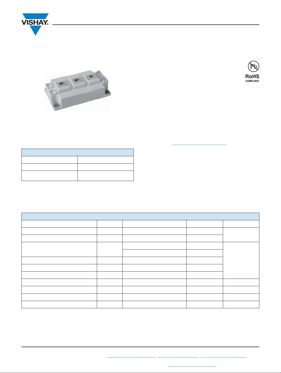
Double INT-A-PAK
2-in-1 Package, 600 V and 400 A
Molding Type Module IGBT,
FEATURES
•Low V
• Low switching losses
• 5 μs short circuit capability
•V
CE(on)
• Maximum junction temperature 175 °C
• Low inductance case
• Fast and soft reverse recovery antiparallel FWD
• Isolated copper baseplate using DCB (Direct Copper
Bonding) technology
• Speed: 0 kHz to 20 kHz
• Material categorization: For definitions of compliance
please see www.vishay.com/doc?99912
trench IGBT technology
CE(on)
with positive temperature coefficient
VS-GT400TH60N
Vishay Semiconductors
PRODUCT SUMMARY
V
CES
at TC = 80 °C 400 A
I
C
(typical)
V
CE(on)
at I
= 400 A, 25 °C
C
600 V
1.60 V
TYPICAL APPLICATIONS
•UPS
• Switching mode power supplies
• Electronic welders
DESCRIPTION
Vishay’s IGBT power module provides ultralow conduction
loss as well as short circuit ruggedness. It is designed for
applications such as UPS and SMPS.
ABSOLUTE MAXIMUM RATINGS (TC = 25 °C unless otherwise noted)
PARAMETER SYMBOL TEST CONDITIONS MAX. UNITS
Collector to emitter voltage V
Gate to emitter voltage V
Collector current I
Pulsed collector current I
Diode continuous forward current I
Diode maximum forward current I
Maximum power dissipation P
Short circuit withstand time t
2
t-value, diode I2tV
I
RMS isolation voltage V
Note
(1)
Repetitive rating: Pulse width limited by maximum junction temperature.
CM
CES
GES
C
F
FM
SC
ISOL
TC = 25 °C 530
= 80 °C 400
T
C
(1)
D
tp = 1 ms 800
TJ = 175 °C 1600 W
TJ = 125 °C 5 μs
= 0 V, t = 10 ms, TJ = 125 °C 10 900 A2s
R
f = 50 Hz, t = 1 min 2500 V
600
± 20
400
800
V
A
Revision: 06-Aug-12
For technical questions within your region: DiodesAmericas@vishay.com
THIS DOCUMENT IS SUBJECT TO CHANGE WITHOUT NOTICE. THE PRODUCTS DESCRIBED HEREIN AND THIS DOCUMENT
ARE SUBJECT TO SPECIFIC DISCLAIMERS, SET FORTH AT www.vishay.com/doc?91000
1
, DiodesAsia@vishay.com, DiodesEurope@vishay.com
Document Number: 93488
VS-GT400TH60N
www.vishay.com
IGBT ELECTRICAL SPECIFICATIONS (TC = 25 °C unless otherwise noted)
PARAMETER SYMBOL TEST CONDITIONS MIN. TYP. MAX. UNITS
Collector to emitter breakdown voltage V
(BR)CES
VGE = 0 V, IC = 2 mA, TJ = 25 °C 600 - -
VGE = 15 V, IC = 400 A, TJ = 25 °C - 1.6 2.05
Gate to emitter threshold voltage V
Zero gate voltage collector current I
Gate to emitter leakage current I
CE(on)
GE(th)
CES
GES
= 15 V, IC = 400 A, TJ = 175 °C - 2.0 -
V
GE
VCE = VGE, IC = 4 mA, TJ = 25 °C 4.0 - 6.5
VCE = V
VGE = V
, VGE = 0 V, TJ = 25 °C - - 5.0 mA
CES
, VCE = 0 V, TJ = 25 °C - - 400 nA
GES
SWITCHING CHARACTERISTICS
PARAMETER SYMBOL TEST CONDITIONS MIN. TYP. MAX. UNITS
Turn-on delay time t
Rise time t
Turn-off delay time t
Fall time t
Turn-on switching loss E
Turn-off switching loss E
Turn-on delay time t
Rise time t
Turn-off delay time t
Fall time t
Turn-on switching loss E
Turn-off switching loss E
Input capacitance C
Reverse transfer capacitance C
SC data I
Internal gate resistance R
Stray inductance L
Module lead resistance, terminal to chip R
d(on)
r
d(off)
f
on
off
d(on)
r
d(off)
f
on
off
ies
oes
res
SC
gint
CE
CC’+EE’
VCC = 400 V, IC = 400 A, Rg = 1.3 ,
V
= ± 15 V, TJ = 25 °C
GE
VCC = 400 V, IC = 400 A, Rg = 1.3 ,
V
= ± 15 V, TJ = 175 °C
GE
VGE = 0 V, VCE = 30 V, f = 1.0 MHz
tsc 5 μs, VGE = 15 V, TJ = 125 °C,
= 360 V, V
V
CC
CEM
600 V
TC = 25 °C - 0.35 - m
Vishay Semiconductors
VCollector to emitter saturation voltage V
-35-
-70-
- 180 -
-75-
- 14.1 -
- 10.0 -
-37-
-72-
- 220 -
-84-
- 23.2 -
- 16.8 -
- 30.8 -
-2.12-
-0.92-
-TBD- A
-1.3-
- - 20 nH
ns
mJ
ns
mJ
nFOutput capacitance C
DIODE ELECTRICAL SPECIFICATIONS (TC = 25 °C unless otherwise noted)
PARAMETER SYMBOL TEST CONDITIONS MIN. TYP. MAX. UNITS
= 25 °C - 1.38 1.80
T
Diode forward voltage V
Diode reverse recovery charge Q
F
rr
IF = 400 A
IF = 400 A, VR = 300 V,
Diode peak reverse recovery current I
Diode reverse recovery energy E
rr
rec
Revision: 06-Aug-12
For technical questions within your region: DiodesAmericas@vishay.com
dI/dt = - 7000 A/μs,
= - 15 V
V
GE
2
, DiodesAsia@vishay.com, DiodesEurope@vishay.com
THIS DOCUMENT IS SUBJECT TO CHANGE WITHOUT NOTICE. THE PRODUCTS DESCRIBED HEREIN AND THIS DOCUMENT
ARE SUBJECT TO SPECIFIC DISCLAIMERS, SET FORTH AT www.vishay.com/doc?91000
J
T
= 125 °C - 1.41 -
J
= 25 °C - 15.5 -
T
J
T
= 125 °C - 28.5 -
J
TJ = 25 °C - 265 -
T
= 125 °C - 335 -
J
TJ = 25 °C - 3.5 -
T
= 125 °C - 7.5 -
J
Document Number: 93488
V
μC
A
mJ
 Loading...