

Page 1

6121 Baker Road,
Suite 108
Minnetonka, MN 55345
www.chtechnology.com
Phone (952) 933-6190
Fax (952) 933-6223
1-800-274-4284
Thank you for downloading this document from C&H Technology, Inc.
Please contact the C&H Technology team for the following questions -
Technical
Application
Assembly
Availability
Pricing
Phone – 1-800-274-4284
E-Mail – sales@chtechnology.com
www.chtechnology.com - SPECIALISTS IN POWER ELECTRONIC COMPONENTS AND ASSEMBLIES - www.chtechnology.com
Page 2
VS180LG..HS05CB Series
Fast Recovery Diodes
Vishay High Power Products
PRODUCT SUMMARY
Junction size Square 180 mils
Wafer size 4"
class 1000/1200 V
V
RRM
Passivation process Glassivated MESA
Reference Vishay HPP
packaged part
16FL Series
FEATURES
• 100 % tested at probe
• Solderable top metal
• Wafer in box, and die in chip carrier
MAJOR RATINGS AND CHARACTERISTICS
PARAMETER SYMBOL TEST CONDITIONS VALUES UNITS
Maximum forward voltage V
Maximum repetitive reverse voltage V
Note
(1)
Nitrogen flow on die edge
RRM
TJ = Ambient, IF = 16 A 1400 mV
FM
(1)
TJ = Ambient, I
= 100 µA 1000/1200 V
RRM
MECHANICAL DATA
Nominal back metal composition (thickness)
Nominal front metal composition (thickness)
Chip dimensions 180 x 180 mils (4.57 x 4.57) - see dimensions (link at the end of datasheet)
Wafer diameter 100 mm, with standard < 110 > flat
Wafer thickness 260 µm
Maximum width of sawing line 45 µm
Reject ink dot size Ø 0.25 mm minimum
Ink dot location See dimensions (link at the end of datasheet)
Recommended storage environment Storage in original container, in desiccated nitrogen, with no contamination
Cr-Ni-Ag (1 kÅ - 4 kÅ - 6 kÅ)
RoHS
COMPLIANT
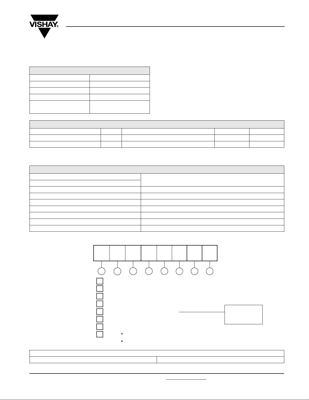
ORDERING INFORMATION TABLE
Device code
Dimensions http://www.vishay.com/doc?95152
Document Number: 93881 For technical questions, contact: die-wafer@vishay.com
Revision: 27-Mar-08 1
VS 180 L G 12 H S05 CB
51324678
1 - Vishay HPP device
2 - Chip dimension in mils
3 - Type of device: L = Fast recovery diode
4 - Passivation process: G = Glassivated MESA
5 - Voltage code x 100 = V
6
- Metallization: H = Silver (anode) - silver (cathode)
7 - Fast recovery type: S05 = 500 ns
8 - CB = Probed uncut die (wafer in box)
None = Probed die in chip carrier
LINKS TO RELATED DOCUMENTS
RRM
Available class
10 = 1000 V
12 = 1200 V
www.vishay.com
 Loading...