

Page 1

6121 Baker Road,
Suite 108
Minnetonka, MN 55345
www.chtechnology.com
Phone (952) 933-6190
Fax (952) 933-6223
1-800-274-4284
Thank you for downloading this document from C&H Technology, Inc.
Please contact the C&H Technology team for the following questions -
Technical
Application
Assembly
Availability
Pricing
Phone – 1-800-274-4284
E-Mail – sales@chtechnology.com
www.chtechnology.com - SPECIALISTS IN POWER ELECTRONIC COMPONENTS AND ASSEMBLIES - www.chtechnology.com
Page 2
www.vishay.com
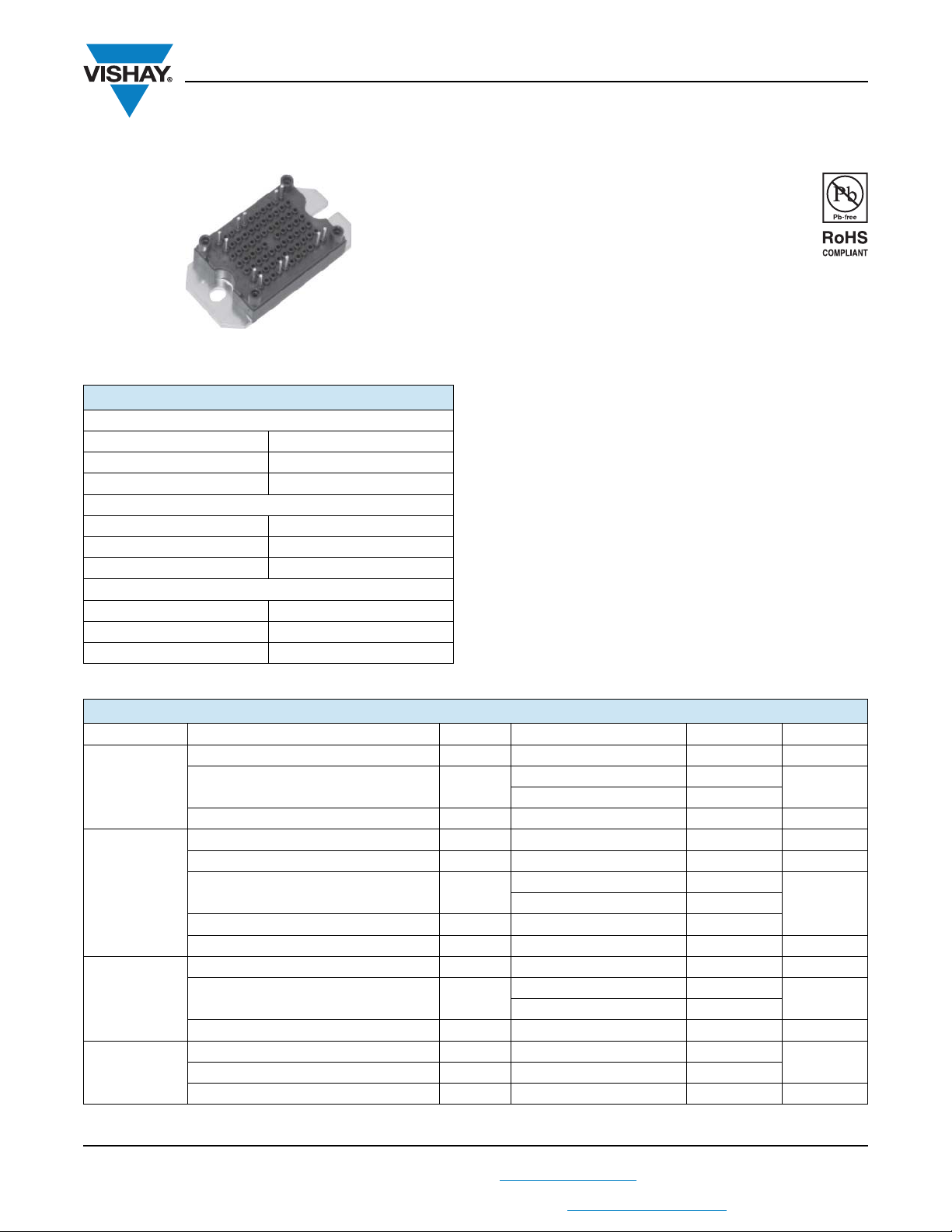
MTP
Primary MTP IGBT Power Module
PRODUCT SUMMARY
FRED Pt® AP DIODE, TJ = 150 °C
V
RRM
at 80 °C 11 A
I
F(DC)
at 25 °C at 60 A 2.08 V
V
F
IGBT, T
V
CES
at 25 °C at 60 A 1.98 V
V
CE(ON)
at 80°C 83 A
I
C
FRED Pt
I
F(DC)
at 25 °C at 60 A 2.06 V
V
F
®
CHOPPER DIODE, TJ = 150 °C
V
R
at 80 °C 17 A
= 150 °C
J
600 V
600 V
600 V
VS-100MT060WDF
Vishay Semiconductors
FEATURES
• Buck PFC stage with warp 2 IGBT and FRED Pt
hyperfast diode
• Integrated thermistor
• Isolated baseplate
• Compliant to RoHS Directive 2011/65/EU
• Very low stray inductance design for high speed operation
• Designed and qualified for industrial level
BENEFITS
• Lower conduction losses and switching losses
• Higher switching frequency up to 150 kHz
• Optimized for welding, UPS, and SMPS applications
• PCB solderable terminals
• Direct mounting to heatsink
®
ABSOLUTE MAXIMUM RATINGS
PARAMETER SYMBOL TEST CONDITIONS MAX. UNITS
FRED Pt
Antiparallel
Diode
IGBT
FRED Pt
Chopper Diode
Revision: 01-Mar-12
THIS DOCUMENT IS SUBJECT TO CHANGE WITHOUT NOTICE. THE PRODUCTS DESCRIBED HEREIN AND THIS DOCUMENT
Repetitive peak reverse voltage V
Maximum continuous forward current
= 150 °C maximum
T
J
Maximum power dissipation P
Collector to emitter voltage V
Gate to emitter voltage V
Maximum continuous collector current
= 15 V, TJ = 150 °C maximum
at V
GE
Clamped inductive load current I
Maximum power dissipation P
Repetitive peak reverse voltage V
Maximum continuous forward current
T
= 150 °C maximum
J
Maximum power dissipation P
Maximum operating junction temperature T
Storage temperature range T
Isolation voltage V
ARE SUBJECT TO SPECIFIC DISCLAIMERS, SET FORTH AT www.vishay.com/doc?91000
RRM
I
F(DC)
RRM
ISOL
CES
GE
I
C
LM
I
F
Stg
TC = 25 °C 17
T
= 80 °C 11
C
TC = 25 °C 25 W
D
TJ = 25 °C 600 V
I
max. ± 250 ns ± 20 V
GES
TC = 25 °C 121
= 80 °C 83
C
TC = 25 °C 462 W
D
TC = 25 °C 26
T
= 80 °C 17
C
TC = 25 °C 56 W
D
J
V
t = 1 s, TJ = 25 °C 3500 V
RMS
1
For technical questions, contact: indmodules@vishay.com
600 V
300
600 V
150
- 40 to + 150
Document Number: 93412
A
AT
A
°C
Page 3
www.vishay.com
ELECTRICAL SPECIFICATIONS (TJ = 25 °C unless otherwise noted)
PARAMETER SYMBOL TEST CONDITIONS MIN. TYP. MAX. UNITS
Blocking voltage BV
AP Diode
Forward voltage drop V
Collector to emitter
breakdown voltage
Temperature coefficient of
breakdown voltage
IGBT
Collector to emitter voltage V
Gate threshold voltage V
Collector to emitter
leakage current
Gate to emitter leakage I
Forward voltage drop V
FRED Pt
Chopper
Blocking voltage BV
Diode
Reverse leakage current I
RECOVERY PARAMETER
Peak reverse recovery current I
AP Diode
Reverse recovery time t
Reverse recovery charge Q
Peak reverse recovery current I
Reverse recovery time t
FRED Pt
Chopper
Diode
Reverse recovery charge Q
Peak reverse recovery current I
Reverse recovery time t
Reverse recovery charge Q
V
RRM
FM
BV
CES
BR(CES)
CE(ON)
GE(th)
I
CES
GES
FM
RM
RM
rr
rr
rr
rr
rr
rr
rr
rr
rr
0.5 mA 600 - - V
IF = 60 A - 2.08 2.43
I
= 60 A, TJ = 125 °C - 2.05 2.3
F
VGE = 0 V, IC = 0.5 mA 600 - - V
/TJIC = 0.5 mA (25 °C to 125 °C) - 0.6 - V/°C
VGE 15 V, IC = 60 A - 1.93 2.29
V
= 15 V, lC = 60 A, TJ = 125 °C - 2.36 2.80
GE
VCE = VGE, IC = 500 μA 2.9 - 6.0 V
VGE = 0 V, VCE = 600 V - - 100 μA
= 0 V, VCE = 600 V, TJ = 125 °C - - 2.0 mA
V
GE
VGE = ± 20 V - - ± 100 nA
IF = 60 A - 2.06 2.53
= 60 A, TJ = 125 °C - 1.83 2.26
F
0.5 mA 600 - -
V
= 600 V - - 75 μA
RRM
V
= 600 V, TJ = 125 °C - - 0.5 mA
RRM
IF = 60 A
dI/dt = 200 A/μs
= 200 V
V
R
IF = 60 A
dI/dt = 200 A/μs
= 200 V
V
R
IF = 60 A
dI/dt = 200 A/μs
V
= 200 V, TJ = 125 °C
R
VS-100MT060WDF
Vishay Semiconductors
V
V
VI
-6711A
- 120 160 ns
- 620 850 nC
-4.56.0A
-6785ns
- 130 250 nC
- 9.5 12.0 A
- 128 165 ns
- 601 900 nC
Revision: 01-Mar-12
2
Document Number: 93412
For technical questions, contact: indmodules@vishay.com
THIS DOCUMENT IS SUBJECT TO CHANGE WITHOUT NOTICE. THE PRODUCTS DESCRIBED HEREIN AND THIS DOCUMENT
ARE SUBJECT TO SPECIFIC DISCLAIMERS, SET FORTH AT www.vishay.com/doc?91000
Page 4
www.vishay.com
SWITCHING CHARACTERISTICS (TJ = 25 °C unless otherwise noted)
PARAMETER SYMBOL TEST CONDITIONS MIN. TYP. MAX. UNITS
PFC IGBT
Total gate charge Q
Gate to drain (Miller) charge Q
Turn-on switching loss E
Total switching loss E
Turn-on delay time t
Rise time t
Turn-off delay time t
Fall time t
Turn-on switching loss E
Total switching loss E
Turn-on delay time t
Rise time t
Turn-off delay time t
Fall time t
Input capacitance C
Reverse transfer capacitance C
gd
on
off
tot
d(on)
d(off)
on
off
tot
d(on)
d(off)
ies
oes
res
g
IC = 60 A
V
= 480 V
V
CC
= 15 V
GE
gs
IC = 100 A, VCC = 360 V, VGE = 15 V
R
= 5 , L = 500 μH, TJ = 25 °C
r
f
g
IC = 100 A, VCC = 360 V, VGE = 15 V
= 5 , L = 500 μH, TJ = 125 °C
R
r
f
g
VGE = 0 V
V
= 30 V
CC
f = 1 MHz
VS-100MT060WDF
Vishay Semiconductors
- 460 -
- 160 -
-70-
-0.2-
-0.96-
-1.16-
- 240 -
-47-
- 240 -
-66-
-0.33-
-1.45-
-1.78-
- 246 -
-50-
- 246 -
-71-
- 9500 -
- 780 -
- 120 -
nCGate to source charge Q
mJTurn-off switching loss E
ns
mJTurn-off switching loss E
ns
pFOutput capacitance C
THERMISTOR ELECTRICAL CHARACTERISTICS (TJ = 25 °C unless otherwise noted)
PARAMETER SYMBOL TEST CONDITIONS MIN. TYP. MAX. UNITS
Resistance R T
B value B T
= 25 °C - 30 000 -
J
= 25 °C/TJ = 85 °C - 4000 - K
J
THERMAL AND MECHANICAL SPECIFICATIONS
PARAMETER SYMBOL MIN. TYP. MAX. UNITS
AP FRED Pt Diode Junction to case diode thermal resistance
IGBT Junction to case IGBT thermal resistance - - 0.27
FRED Pt
Chopper Diode
Junction to case diode thermal resistance - - 2.25
Case to sink, flat, greased surface per module R
Mounting torque ± 10 % to heatsink
(1)
R
thJC
thCS
Approximate weight - 65 - g
Note
(1)
A mounting compound is recommended and the torque should be rechecked after a period of 3 hours to allow for the spread of the
compound.
--4.9
°C/W
-0.06-°C/W
--4Nm
Revision: 01-Mar-12
3
Document Number: 93412
For technical questions, contact: indmodules@vishay.com
THIS DOCUMENT IS SUBJECT TO CHANGE WITHOUT NOTICE. THE PRODUCTS DESCRIBED HEREIN AND THIS DOCUMENT
ARE SUBJECT TO SPECIFIC DISCLAIMERS, SET FORTH AT www.vishay.com/doc?91000
Page 5

www.vishay.com
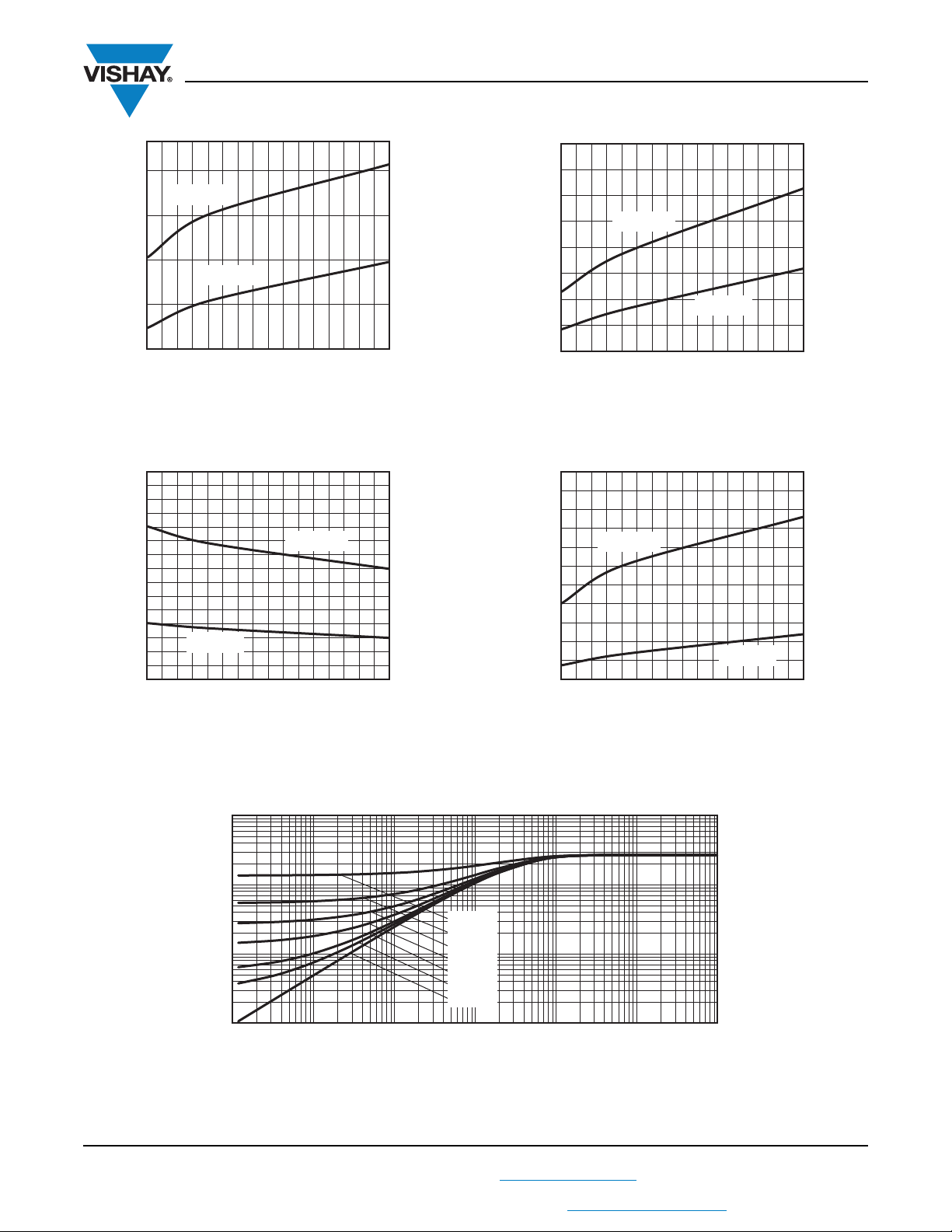
I
C
(A)
VCE (V)
1 10 100 1000
0.01
0.1
1
93412_02
1000
10
100
I
C
(A)
VCE (V)
012345
0
93412_03
250
50
150
100
200
VGE = 9 V
VGE = 12 V
VGE = 15 V
VGE = 18 V
I
C
(A)
VCE (V)
012345
0
93412_04
250
50
150
100
200
VGE = 9 V
VGE = 12 V
VGE = 15 V
VGE = 18 V
I
CES
(mA)
V
CES
(V)
100 600200 300 400 500
0.0001
0.001
93412_06
10
1
0.1
0.01
150 °C
25 °C
160
140
120
100
80
60
40
Maximum Allowable
Case Temperature (°C)
20
0
0
93412_01
IC - Continuous Collector Current (A)
Fig. 1 - Maximum IGBT Continuous Collector Current vs.
Case Temperature
80 100604020
VS-100MT060WDF
Vishay Semiconductors
140120
Fig. 4 - Typical IGBT Output Characteristics, T
250
200
= 125 °C
J
Fig. 2 - IGBT Reverse BIAS SOA T
= 150 °C, VGE = 15 V
J
TC = 125 °C
TC = 25 °C
(A)
C
I
150
100
50
0
5678910
93412_05
VGE (V)
Fig. 5 - Typical IGBT Transfer Characteristics, T
= 125 °C
J
Fig. 3 - Typical IGBT Output Characteristics, T
Revision: 01-Mar-12
THIS DOCUMENT IS SUBJECT TO CHANGE WITHOUT NOTICE. THE PRODUCTS DESCRIBED HEREIN AND THIS DOCUMENT
ARE SUBJECT TO SPECIFIC DISCLAIMERS, SET FORTH AT www.vishay.com/doc?91000
= 25 °C
J
Fig. 6 - Typical IGBT Zero Gate Voltage Collector Current
4
For technical questions, contact: indmodules@vishay.com
Document Number: 93412
Page 6

5.0
93412_09
IF - Continuous Forward Current (A)
Allowable Case Temperature (°C)
0
20
40
60
80
100
120
140
160
0 5 10 15 20
I
F
- Instantaneous Forward Drop (A)
VF - Forward Voltage Drop (V)
0.25 0.75 1.25 2.251.75 2.75 3.753.25
0
90
30
50
70
40
10
20
60
80
100
93412_10
TJ = 150 °C
TJ = 125 °C
TJ = 25 °C
I
R
(mA)
VR (V)
100 200 300 400 500 600
0.00001
0.001
0.0001
0.01
0.1
93412_12
TJ = 150 °C
TJ = 25 °C
www.vishay.com
VS-100MT060WDF
Vishay Semiconductors
TJ = 25 °C
TJ = 125 °C
IC (mA)
(V)
geth
V
93412_07
4.5
4.0
3.5
3.0
0.2 1.00.3 0.4 0.6 0.80.5 0.7 0.9
Fig. 7 - Typical IGBT Gate Thresold Voltage
100
90
80
70
60
50
40
30
20
10
- Instantaneous Forward Current (A)
F
I
93412_08
0
0.5 1.0 1.5 2.0 2.5 3.0
TJ = 150 °C
TJ = 125 °C
TJ = 25 °C
VF - Anode to Cathode
Forward Voltage Drop (V)
Fig. 8 - Typical Diode Forward Voltage Characteristics of
Antiparallel Diode, t
= 500 μs
p
Fig. 10 - Typical PFC Diode Forward Voltage
160
140
120
100
80
60
40
20
Allowable Case Temperature (°C)
0
0 5 10 15 20 25 30 35 40
93412_11
IF - Continuous Forward Current (A)
Fig. 11 - Maximum Continuous Forward Current vs.
Case Temperature PFC Diode
Revision: 01-Mar-12
Fig. 9 - Maximum Continuous Forward Current vs.
Case Temperature Antiparallel Diode
THIS DOCUMENT IS SUBJECT TO CHANGE WITHOUT NOTICE. THE PRODUCTS DESCRIBED HEREIN AND THIS DOCUMENT
ARE SUBJECT TO SPECIFIC DISCLAIMERS, SET FORTH AT www.vishay.com/doc?91000
Fig. 12 - Typical FRED Pt Chopper Diode Reverse Current vs.
5
For technical questions, contact: indmodules@vishay.com
Reverse Voltage
Document Number: 93412
Page 7

www.vishay.com
Energy (mJ)
IC (A)
020 608010040 120
0
93412_13
2.0
1.2
1.6
0.8
0.4
E
on
E
off
Switching Time (ns)
IC (A)
020 8040 10060 120
10
93412_15
1000
100
t
d(off)
t
d(on)
t
f
t
r
t
rr
(ns)
dIF/dt (A/μs)
100 200 300 400
93412_17
500
100
150
250
200
TJ = 25 °C
TJ = 125 °C
I
rr
(A)
dIF/dt (A/μs)
100 200 300 400
93412_18
500
0
25
20
10
15
5
TJ = 25 °C
TJ = 125 °C
VS-100MT060WDF
Vishay Semiconductors
TJ = 125 °C, VCC = 360 V, VGE = 15 V, L = 500 μH, Rg = 5
Fig. 13 - Typical IGBT Energy Loss vs. I
5
4
3
E
off
2
Energy (mJ)
1
E
on
C
1000
100
t
f
t
r
t
d(off)
t
d(on)
Switching Time (ns)
10
010 304020 50
93412_16
Rg (Ω)
Fig. 16 - Typical IGBT Switching Time vs. R
I
= 100 A, VCE = 360 V, VGE = 15 V, L = 500 μH
C
, TJ = 125 °C
g
93412_14
Revision: 01-Mar-12
0
0 1020304050
Rg (Ω)
Fig. 14 - Typical IGBT Energy Loss vs. R
I
= 100 A, VCC = 360 V, VGE = 15 V, L = 500 μH, Rg = 5
C
Fig. 15 - Typical IGBT Switching Time vs. I
TJ = 125 °C, VDD = 360 V, VGE = 15 V, L = 500 μH, Rg = 5
, TJ = 125 °C
g
C
Fig. 17 - Typical t
Fig. 18 - Typical I
6
Antiparallel Diode vs. dIF/dt
rr
V
= 200 V, IF = 60 A
rr
Antiparallel Diode vs. dIF/dt
rr
V
= 200 V, IF = 60 A
rr
Document Number: 93412
For technical questions, contact: indmodules@vishay.com
THIS DOCUMENT IS SUBJECT TO CHANGE WITHOUT NOTICE. THE PRODUCTS DESCRIBED HEREIN AND THIS DOCUMENT
ARE SUBJECT TO SPECIFIC DISCLAIMERS, SET FORTH AT www.vishay.com/doc?91000
Page 8
(nC)
t
rr
(ns)
dIF/dt (A/μs)
100 200 300 400
93412_20
500
30
80
180
130
TJ = 25 °C
TJ = 125 °C
I
rr
(A)
dIF/dt (A/μs)
100 200 300 400
93412_21
500
0
20
10
15
5
TJ = 25 °C
TJ = 125 °C
Q
rr
(nC)
dIF/dt (A/μs)
100 200 300 400
93412_22
500
0
1100
400
600
900
1000
200
300
500
700
800
100
TJ = 25 °C
TJ = 125 °C
0.001
0.01
0.1
1
0.00001
93412_23
0.0001 0.001 0.01 0.1 1
t1 - Rectangular Pulse Duration (s)
Z
thJC
- Thermal Impedance
Junction to Case (°C/W)
10
D = 0.50
D = 0.20
D = 0.10
D = 0.05
D = 0.02
D = 0.01
DC
rr
Q
93412_19
www.vishay.com
1500
TJ = 125 °C
1200
900
600
300
100 200 300 400
Fig. 19 - Typical Qrr Antiparallel Diode vs. dIF/dt
TJ = 25 °C
dIF/dt (A/μs)
V
= 200 V, IF = 60 A
rr
500
Vishay Semiconductors
Fig. 21 - Typical I
V
= 200 V, IF = 60 A
rr
VS-100MT060WDF
Chopper Diode vs. dIF/dt
rr
Revision: 01-Mar-12
Fig. 20 - Typical t
Chopper Diode vs. dIF/dt
rr
V
= 200 V, IF = 60 A
rr
Fig. 23 - Maximum Thermal Impedance Z
7
Fig. 22 - Typical Q
Characteristics (IGBT)
thJC
Chopper Diode vs. dIF/dt
rr
V
= 200 V, IF = 40 A
rr
Document Number: 93412
For technical questions, contact: indmodules@vishay.com
THIS DOCUMENT IS SUBJECT TO CHANGE WITHOUT NOTICE. THE PRODUCTS DESCRIBED HEREIN AND THIS DOCUMENT
ARE SUBJECT TO SPECIFIC DISCLAIMERS, SET FORTH AT www.vishay.com/doc?91000
Page 9
www.vishay.com
93412_24
Z
thJC
-
Thermal Impedance
Junction to Case (°C/W)
t1 - Rectangular Pulse Duration (s)
0.01
0.1
1
10
0.0001 0.001 0.01 0.1 1 10
D = 0.02
D = 0.01
DC
D = 0.05
D = 0.10
D = 0.20
D = 0.50
L
80 V
R
g
1000 V
D.U.T.
+
-
R
g
D.U.T.
R =
V
CC
I
CM
V
CC
+
-
VS-100MT060WDF
Vishay Semiconductors
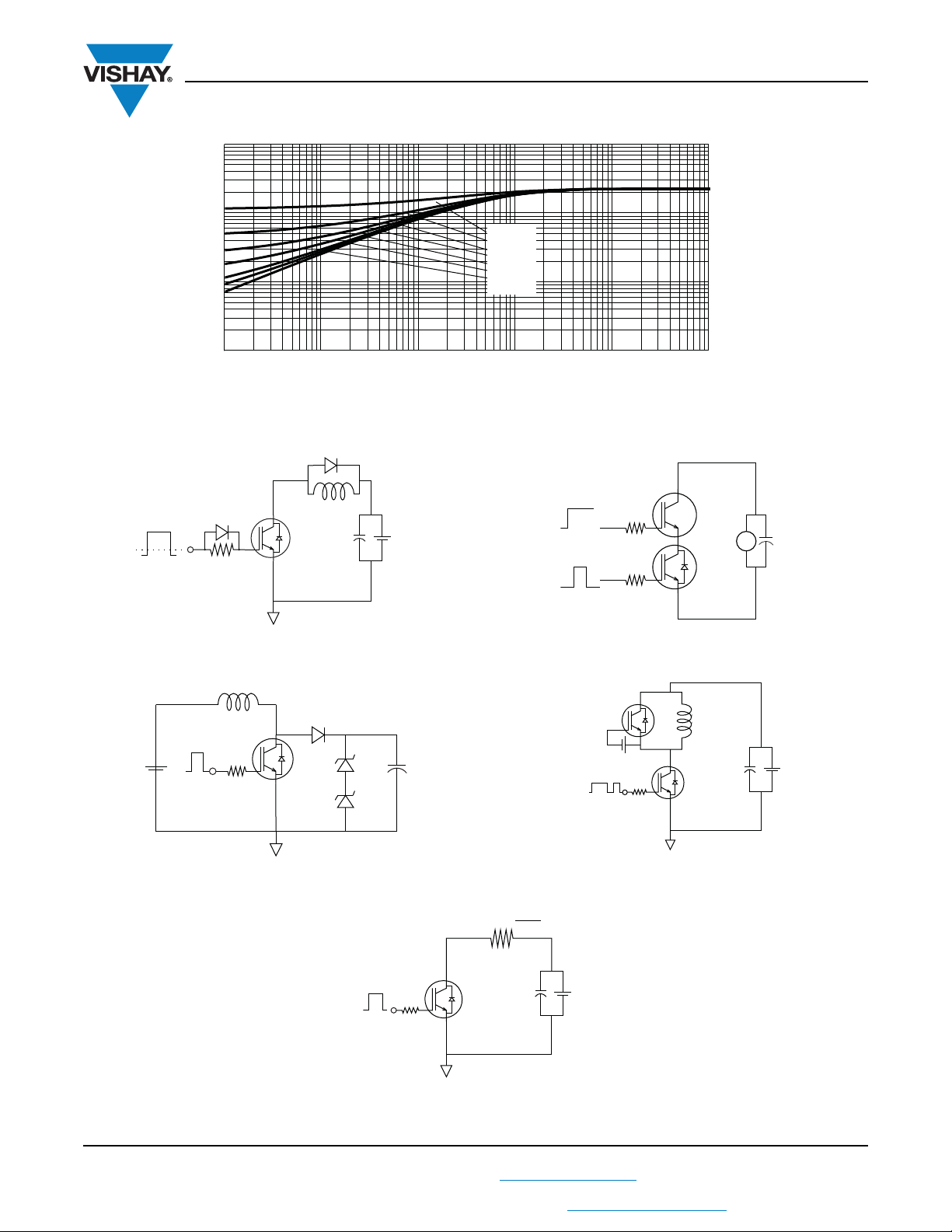
Fig. 24 - Maximum Thermal Impedance Z
0
1K
D.U.T.
Fig. C.T.1 - Gate Charge Circuit (Turn-Off)
Characteristics (PFC Diode)
thJC
Driver
L
V
CC
+
-
D.U.T.
D
+
C
900 V
-
Fig. C.T.3 - S.C. SOA Circuit
Diode clamp/
D.U.T.
-
- 5 V
+
R
g
L
D.U.T./
Driver
+
-
V
CC
Fig. C.T.2 - RBSOA Circuit
Revision: 01-Mar-12
Fig. C.T.5 - Resistive Load Circuit
For technical questions, contact: indmodules@vishay.com
THIS DOCUMENT IS SUBJECT TO CHANGE WITHOUT NOTICE. THE PRODUCTS DESCRIBED HEREIN AND THIS DOCUMENT
ARE SUBJECT TO SPECIFIC DISCLAIMERS, SET FORTH AT www.vishay.com/doc?91000
Fig. C.T.4 - Switching Loss Circuit
8
Document Number: 93412
Page 10

www.vishay.com
CIRCUIT CONFIGURATION
DIMENSIONS in millimeters
VS-100MT060WDF
Vishay Semiconductors
E1
F1
Q1
D1
A7
E6
E7
Th
G6
I1
L1
D2
A1
B1
Q4
G7
M7
D3
M2
M3
D4
19.8 ± 0.1
12 ± 0.3 12.1± 0.3
2.5 ± 0.1
0.8 Ra
1.3 7.4
45°
Ø 2.1(X4)
39.5 ± 0.3
Ø 1.1± 0.025
45 ± 0.1
63.5 ± 0.15
48.7± 0.3
BACDEF LG HI M
1
2
3
4
5
6
7
6
12
18
24
30
3.0
2.1
1.5
z detail
6
3
17± 0.3
7.6
22.8
15.2
X
5.2
R 2.6 (X2)
Use Self Tapping Screw
or M2.5 x X.
e.g. M2.5 x 6 or M2.5 x 8
according to Pcb
thickness used
21.1 ± 0.5
33.2 ± 0.3
31.8 ± 0.15
4.1
Diam. 5 (X4)
27.5 ± 0.3
PINS POSITION
WITH TOLERANCE
Ø 0.6
LINKS TO RELATED DOCUMENTS
Dimensions www.vishay.com/doc?95383
Revision: 01-Mar-12
9
Document Number: 93412
For technical questions, contact: indmodules@vishay.com
THIS DOCUMENT IS SUBJECT TO CHANGE WITHOUT NOTICE. THE PRODUCTS DESCRIBED HEREIN AND THIS DOCUMENT
ARE SUBJECT TO SPECIFIC DISCLAIMERS, SET FORTH AT www.vishay.com/doc?91000
Page 11

DIMENSIONS in millimeters
48.7 ± 0.3
A
1
2
3
4
5
6
7
BCDE GH I LM
19.8 ± 0.1
45°
Ø 2.1 (x 4)
7.4
22.8
15.2
7.6
5.2
7
1.3
6
12
18
24
30
20
R2.6 (x 2)
Ø 1 ± 0.025
F
Pins position
with tolerance
Ø 0.5
Ø 5 (x 4)
21.1
+ 0.5
- 0.2
22.8 ± 0.5
Ground pin
31.8 ± 0.15
33.2 ± 0.3
27.5 ± 0.3
4.1
39.5 ± 0.3 12 ± 0.312 ± 0.3
2.5 ± 0.1
17 ± 0.3
3
0.8 Ra
Ø 1.1 ± 0.025
45 ± 0.1
63.5 ± 0.15
1.5
Use self taping screw
or M2.5 x X.
e.g. M2.5 x 6 or M2.5 x 8
according to PCB thickness used
z detail
3.0
2.1
6
Outline Dimensions
Vishay Semiconductors
MTP - Full Pin
Document Number: 95383 For technical questions, contact: indmodules@vishay.com
Revision: 19-Nov-10 1
www.vishay.com
Page 12

Legal Disclaimer Notice
www.vishay.com
Vishay
Disclaimer
ALL PRODUCT, PRODUCT SPECIFICATIONS AND DATA ARE SUBJECT TO CHANGE WITHOUT NOTICE TO IMPROVE
RELIABILITY, FUNCTION OR DESIGN OR OTHERWISE.
Vishay Intertechnology, Inc., its affiliates, agents, and employees, and all persons acting on its or their behalf (collectively,
“Vishay”), disclaim any and all liability for any errors, inaccuracies or incompleteness contained in any datasheet or in any other
disclosure relating to any product.
Vishay makes no warranty, representation or guarantee regarding the suitability of the products for any particular purpose or
the continuing production of any product. To the maximum extent permitted by applicable law, Vishay disclaims (i) any and all
liability arising out of the application or use of any product, (ii) any and all liability, including without limitation special,
consequential or incidental damages, and (iii) any and all implied warranties, including warranties of fitness for particular
purpose, non-infringement and merchantability.
Statements regarding the suitability of products for certain types of applications are based on Vishay’s knowledge of typical
requirements that are often placed on Vishay products in generic applications. Such statements are not binding statements
about the suitability of products for a particular application. It is the customer’s responsibility to validate that a particular
product with the properties described in the product specification is suitable for use in a particular application. Parameters
provided in datasheets and/or specifications may vary in different applications and performance may vary over time. All
operating parameters, including typical parameters, must be validated for each customer application by the customer’s
technical experts. Product specifications do not expand or otherwise modify Vishay’s terms and conditions of purchase,
including but not limited to the warranty expressed therein.
Except as expressly indicated in writing, Vishay products are not designed for use in medical, life-saving, or life-sustaining
applications or for any other application in which the failure of the Vishay product could result in personal injury or death.
Customers using or selling Vishay products not expressly indicated for use in such applications do so at their own risk and agree
to fully indemnify and hold Vishay and its distributors harmless from and against any and all claims, liabilities, expenses and
damages arising or resulting in connection with such use or sale, including attorneys fees, even if such claim alleges that Vishay
or its distributor was negligent regarding the design or manufacture of the part. Please contact authorized Vishay personnel to
obtain written terms and conditions regarding products designed for such applications.
No license, express or implied, by estoppel or otherwise, to any intellectual property rights is granted by this document or by
any conduct of Vishay. Product names and markings noted herein may be trademarks of their respective owners.
Material Category Policy
Vishay Intertechnology, Inc. hereby certifies that all its products that are identified as RoHS-Compliant fulfill the
definitions and restrictions defined under Directive 2011/65/EU of The European Parliament and of the Council
of June 8, 2011 on the restriction of the use of certain hazardous substances in electrical and electronic equipment
(EEE) - recast, unless otherwise specified as non-compliant.
Please note that some Vishay documentation may still make reference to RoHS Directive 2002/95/EC. We confirm that
all the products identified as being compliant to Directive 2002/95/EC conform to Directive 2011/65/EU.
Revision: 12-Mar-12
1
Document Number: 91000
 Loading...