

Page 1

6121 Baker Road,
Suite 108
Minnetonka, MN 55345
www.chtechnology.com
Phone (952) 933-6190
Fax (952) 933-6223
1-800-274-4284
Thank you for downloading this document from C&H Technology, Inc.
Please contact the C&H Technology team for the following questions -
Technical
Application
Assembly
Availability
Pricing
Phone – 1-800-274-4284
E-Mail – sales@chtechnology.com
www.chtechnology.com - SPECIALISTS IN POWER ELECTRONIC COMPONENTS AND ASSEMBLIES - www.chtechnology.com
Page 2
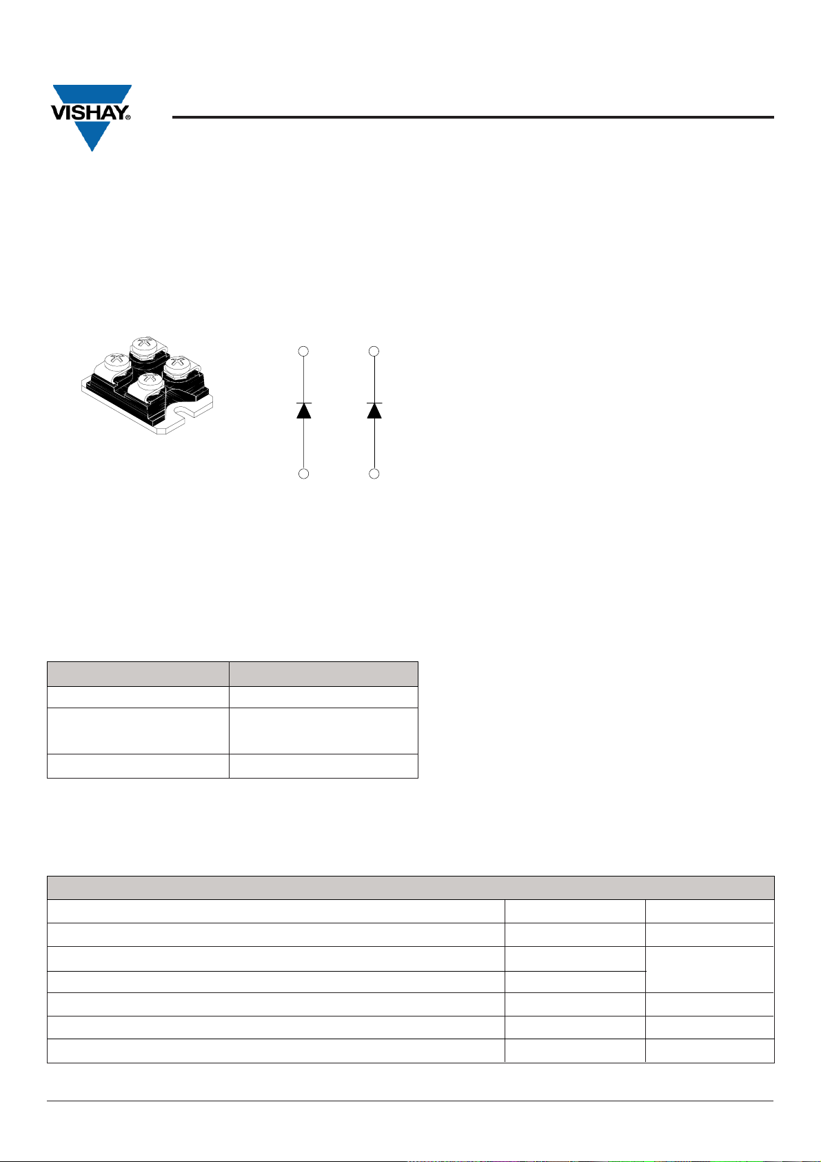
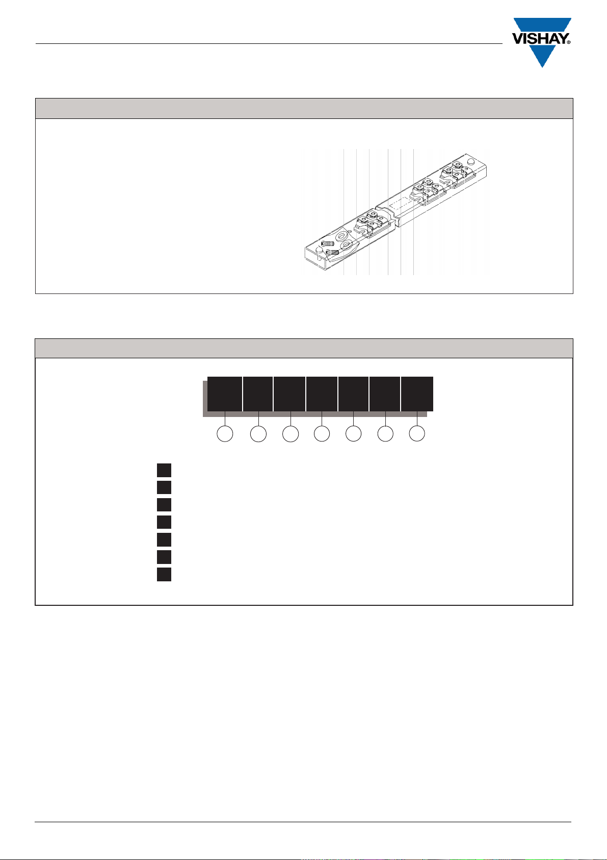
SOT-227
2
4
3
Vishay High Power Products
INSULATED ULTRAFAST
RECTIFIER MODULE
FEATURES
• Two Fully Independent Diodes
• Ceramic Fully Insulated Package (V
1
• Ultrafast Reverse Recovery
• Ultrasoft Reverse Recovery Current Shape
• Low Forward Voltage
• Optimized for Power Conversion: Welding and
Industrial SMPS Applications
• Industry Standard Outline
• Plug-in Compatible with other SOT-227 Packages
• Easy to Assemble
• Direct Mounting to Heatsink
• TOTALLY LEAD-FREE
UFL200FA60P
= 2500V AC)
ISOL
PRODUCT SUMMARY
t
rr
I
F(AV)
@ T
C
V
R
ABSOLUTE MAXIMUM RATINGS
PARAMETERS MAX UNITS
V
I
F
I
FSM
P
V
T
R
D
ISOL
J
Collector-to-Anode Voltage 600 V
Continuos Forward Current, per Diode @ TC = 85°C 144 A
Single Pulse Forward Current, per Diode @ TC = 25°C 1000
Maximum Power Dissipation, per Module @ TC = 85°C 360 W
Isolation Voltage, Any Terminal to Case, t = 1 min 2500 V
Operating Junction and Storage Temperatures -55 to 175 °C
102ns
200A
105°C
600V
DESCRIPTION
The UFL200FA60P insulated modules integrate two
state-of-the-art International Rectifier's Ultrafast
recovery rectifiers in the compact, industry standard
SOT-227 package. The planar structure of the diodes,
and the platinum doping life-time control, provide a
Ultrasoft recovery current shape, together with the
best overall performance, ruggedness and reliability
characteristics.
These devices are thus intended for high frequency
applications in which the switching energy is designed
not to be predominant portion of the total energy, such
as in the output rectification stage of Welding machines,
SMPS, DC-DC converters. Their extremely optimized
stored charge and low recovery current reduce both
over dissipation in the switching elements (and
snubbers) and EMI/ RFI.
Document Number: I27322
Revision: 30-Oct-07
www.vishay.com
1
Page 3
UFL200FA60P
Vishay Semiconductor Italy
ELECTRICAL CHARACTERISTICS @ TJ = 25°C (UNLESS OTHERWISE SPECIFIED)
PARAMETERS MIN TYP MAX UNITS TETS CONDITIONS
V
BR
Cathode Anode 600 - - V IR = 100μA
Breakdown Voltage
V
FM
Forward Voltage - 1.28 1.44 V IF = 100A
- 1.48 1.66 V IF = 200A
- 1.13 1.24 V IF = 100A, TJ = 125°C
- 1.37 1.55 V IF = 200A
I
RM
Reverse Leakage Current - 5 100 μAVR = VR Rated
- 0.2 1 mA TJ = 175°C, VR = VR Rated
C
T
Junction Capacitance - 80 - pF VR = 600V
DYNAMIC RECOVERY CHARACTERISTICS @ TJ = 25°C (UNLESS OTHERWISE SPECIFIED)
PARAMETERS MIN TYP MAX UNITS TETS CONDITIONS
t
rr
I
RRM
Reverse Recovery Time 102 141 ns TJ = 25°C
- 210 293 TJ = 125°C
Peak Recovery Current - 9 12 A TJ = 25°C
I
= 50A
F
VR = 200V
diF /dt = 200A/μs
-2125 TJ = 125°C
Q
rr
Reverse Recovery Charge - 443 744 nC TJ = 25°C
- 2086 3355 TJ = 125°C
THERMAL-MECHANICAL SPECIFICATIONS
PARAMETERS MIN TYP MAX Units
R
thJC
Junction to Case, Single Leg Conducting 0.5 °C/W
Both Leg Conducting 0.25 K/W
R
thCS
Case to Heat Sink, Flat, Greased Surface 0.05
Wt Weight 30 g
T Mounting Torque 1.3 (N•m)
www.vishay.com
2
Document Number: I27322
Revision 30-Oct-07
Page 4
UFL200FA60P
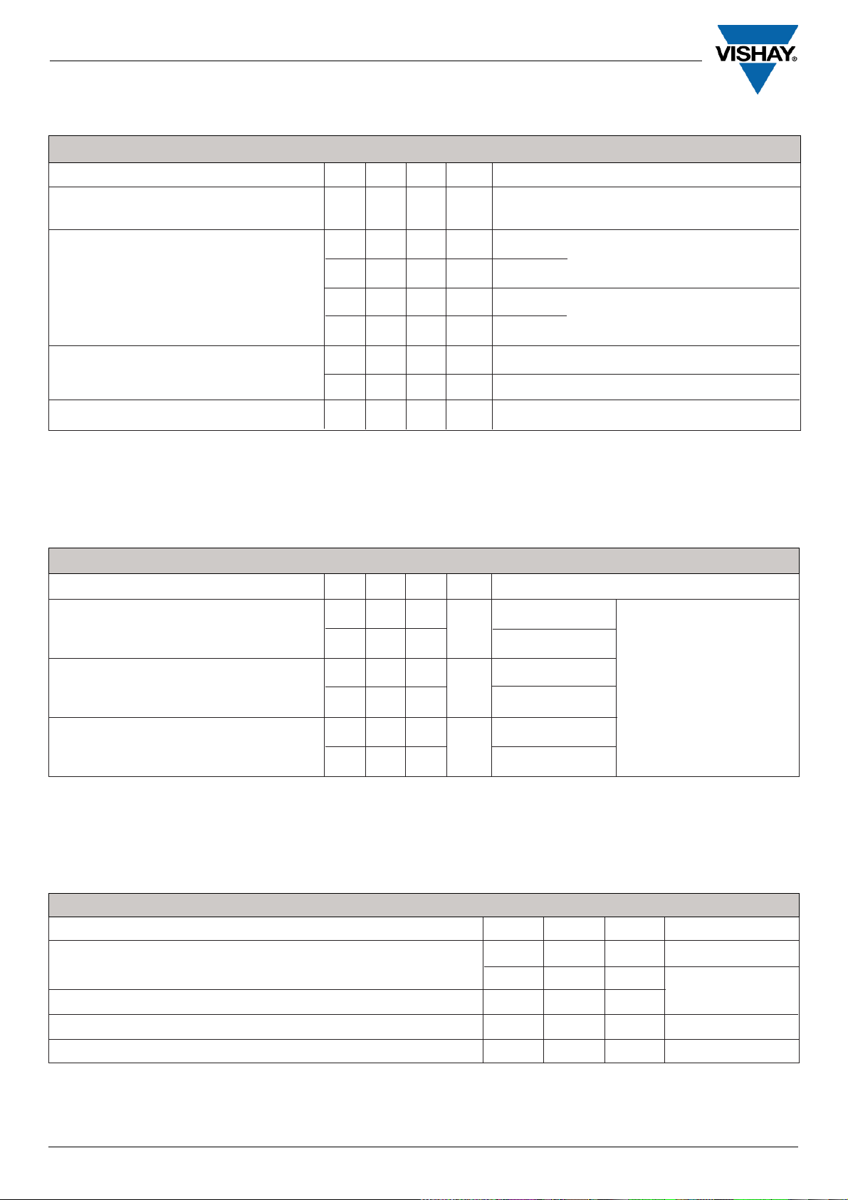
10
100
1000
10000
10 100 1000
T = 25˚C
J
0
1
0.0001 0.001 0.01 0.1 1 10
Vishay Semiconductor Italy
1000
(A)
F
100
Tj = 175°C
10
Tj = 125°C
Instantaneous Forward Current - I
1000
175°C
100
( μA)
R
10
1
0.1
Reverse Current - I
0.01
0.001
100 200 300 400 500 600
Reverse Voltage - VR (V)
(pF)
T
125C
25°C
Tj = 25°C
1
0.0 0.5 1.0 1.5 2.0 2.5
Forward Voltage Drop - VF (V)
Fig. 1 - Typical Forward Voltage Drop Characteristics
(per diode)
(°C/W)
thJC
0.1
Single Pulse
(Thermal Resistance)
Thermal Impedance Z
Junction Capacitance - C
Reverse Voltage - VR (V)
Fig. 3 - Typical Junction Capacitance
Vs. Reverse Voltage
P
DM
t
1
t
2
Notes:
1. Duty factor D = t1/ t2
2. Peak Tj = Pdm x ZthJC + Tc
.01
t 1, Rectangular Pulse Duration (Seconds)
Fig. 4 - Max. Thermal Impedance Z
Document Number: I27322
Revision 30-Oct-07
Characteristics (per diode)
thJC
www.vishay.com
3
Page 5
UFL200FA60P
Vishay Semiconductor Italy
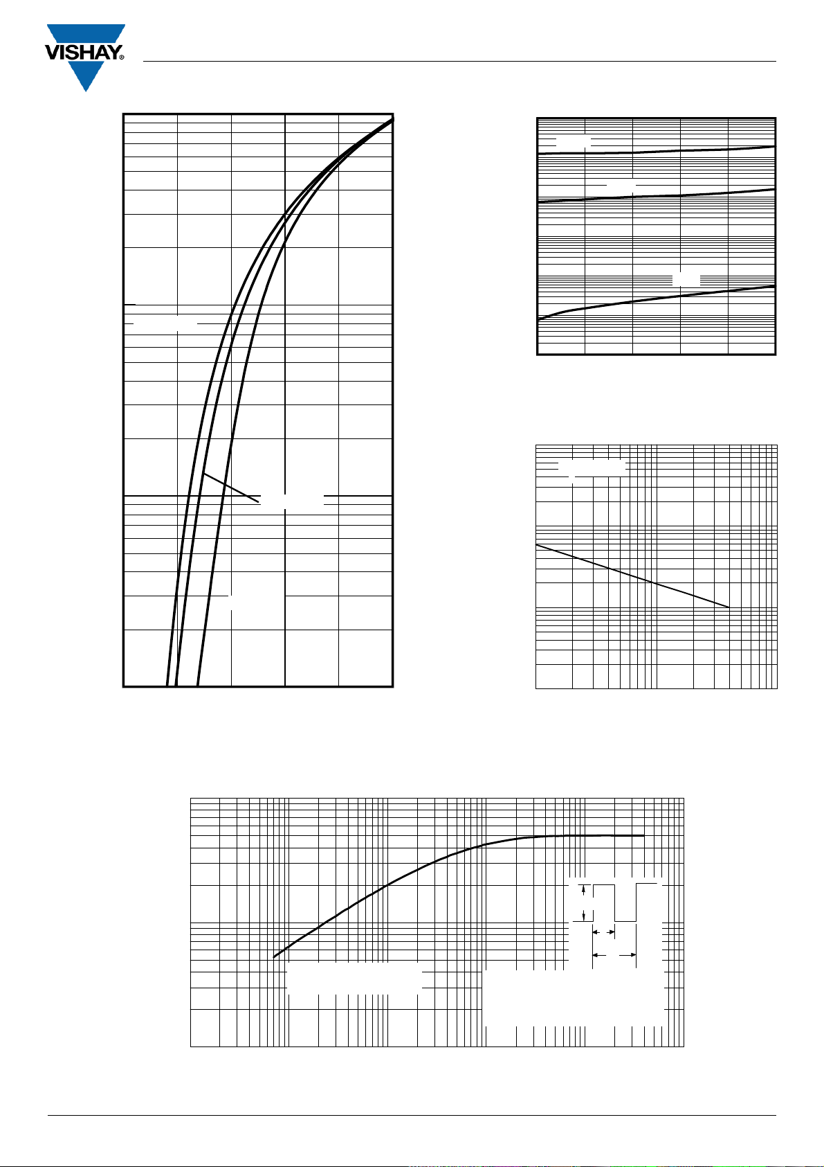
200
150
100
50
Square wave (D=0.50)
80% rated Vr applied
Allowable Case Temperature (°C)
see note
DC
0
0 50 100 150 200 250
Average Forward Current - I
Fig. 5 - Max. Allowable Case Temperature
Vs. Average Forward Current (per leg)
250
Vr = 200V
F(AV)
(A)
180
150
120
RMS Limit
90
60
30
Average Power Loss ( W )
0
DC
D = 0.01
D = 0.02
D = 0.05
D = 0.1
D = 0.2
0 25 50 75 100 125 150
Average Forward Current - I
F(AV)
(A)
Fig. 6 - Forward Power Loss Characteristics
(per leg)
3500
Vr = 200V
3000
200
150
If = 50A, 125°C
trr ( ns )
di
/dt (A/μs )
F
If = 50A, 25°C
100
50
100 1000
Fig. 7 - Typical Reverse Recovery time vs. di
2500
2000
1500
Qrr ( nC )
1000
500
0
If = 50A, 125°C
If = 50A, 25°C
100 1000
di F /dt (A/μs )
/dt
F
Fig. 8 - Typical Stored Charge vs. di
/dt
F
www.vishay.com
4
Document Number: I27322
Revision 30-Oct-07
Page 6
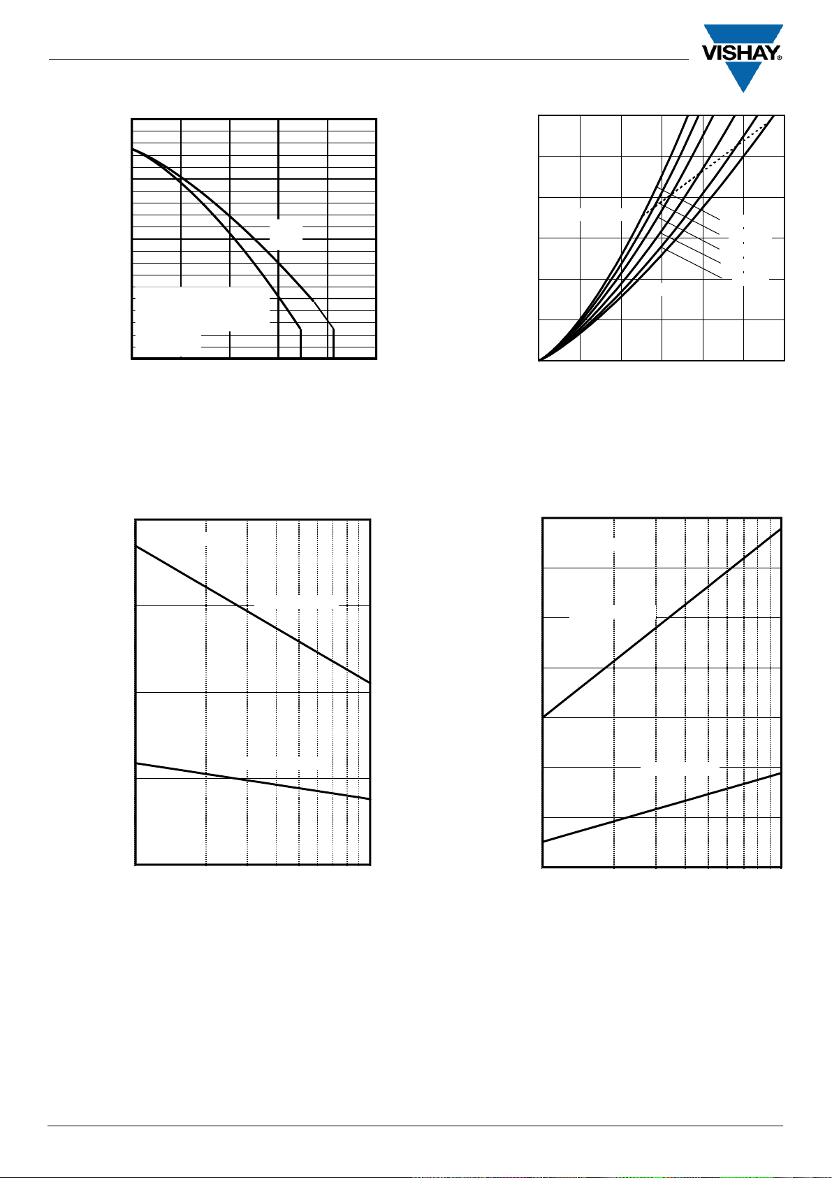
50
40
30
Irr ( A )
20
10
UFL200FA60P
Vishay Semiconductor Italy
Vr = 200V
If = 50A, 125°C
If = 50A, 25°C
dif/dt
ADJUST
V = 200V
L = 70µH
G
R
0
100 1000
di F /dt (A/μs )
Fig. 9 - Typical Stored Current vs. di
0
Ω
0.01
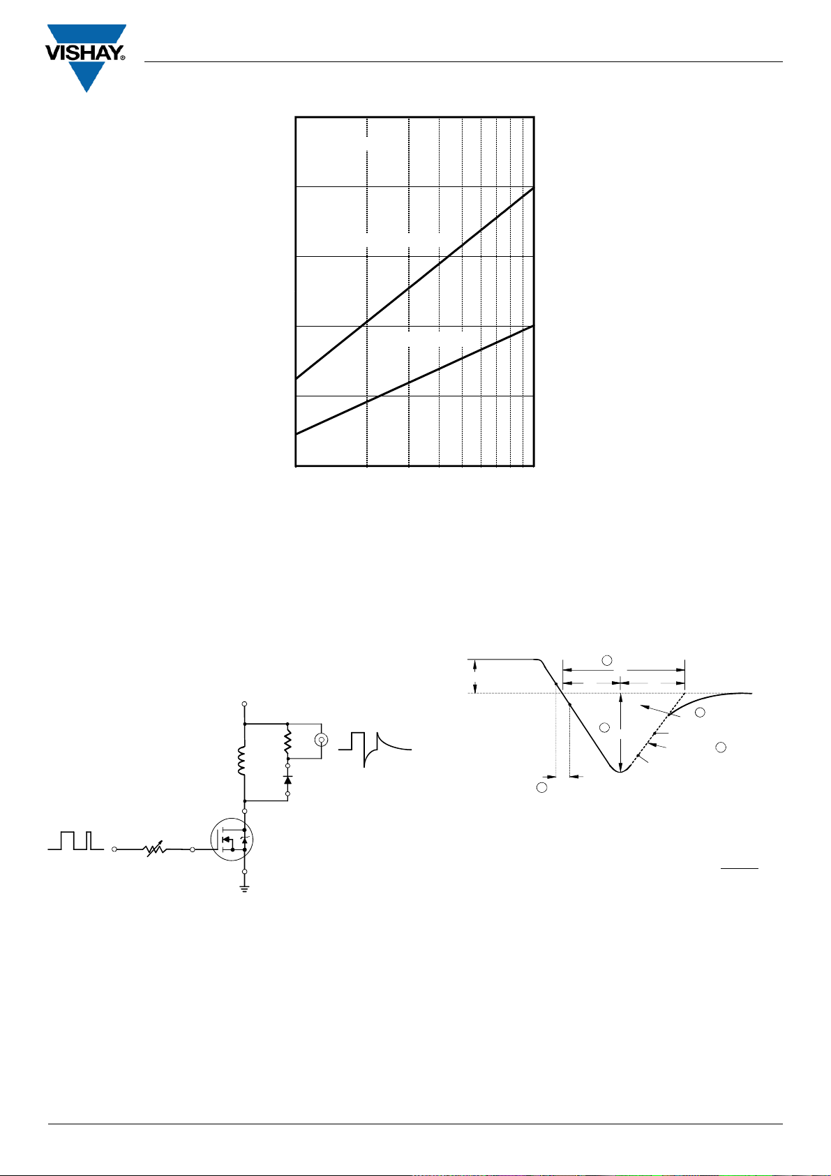
D.U.T.
D
IRFP250
S
1. diF/dt - Rate of change of current through
zero crossing
2. I
- Peak reverse recovery current
RRM
- Reverse recovery time measured from
3. t
rr
zero crossing point of negative going I
point where a line passing through 0.75 I
and 0.50 I
RRM
/dt
F
I
F
1
di /dt
f
F
extrapolated to zero current
RRM
3
t
rr
t
a
2
to
t
b
Q
I
RRM
0.75
4. Qrr - Area under curve defined by
t
and I
rr
5. di
(rec) M
portion of t
rr
0.5
I
RRM
di(rec)M/dt
I
RRM
RRM
/ dt - Peak rate of change
of current during t
rr
4
5
t rr x I
Q
RRM
=
rr
2
b
Fig. 10 - Reverse Recovery Parameter Test
Circuit
Document Number: I27322
Revision 30-Oct-07
Fig. 11 - Reverse Recovery Waveform and Defini-
tions
www.vishay.com
5
Page 7
UFL200FA60P
Vishay Semiconductor Italy
SOT-227 PACKAGE DETAILS
Tube
QUANTITY PER TUBE IS 10
M4 SCREW AND WASHER INCLUDED
ORDERING INFORMATION TABLE
Device Code
1 - ULTRAFAST RECTIFIER
2 - Ultrafast Pt low V
3 - Current Rating (200 = 200A)
4 - Circuit Configuration (2 separate Diodes, parallel pin-out)
5 - Package Indicator (SOT-227 Standard Isolated Base)
6 - Voltage Rating (60 = 600V)
7 - P = Lead-Free
UF L 200 F A 60 P
1 5
24
F
63
7
www.vishay.com
6
Document Number: I27322
Revision 30-Oct-07
Page 8

LEAD ASSIGNMENTS
 Loading...