


6121 Baker Road,
Suite 108
Minnetonka, MN 55345
www.chtechnology.com
Phone (952) 933-6190
Fax (952) 933-6223
1-800-274-4284
Thank you for downloading this document from C&H Technology, Inc.
Please contact the C&H Technology team for the following questions -
Technical
Application
Assembly
Availability
Pricing
Phone – 1-800-274-4284
E-Mail – sales@chtechnology.com
www.chtechnology.com - SPECIALISTS IN POWER ELECTRONIC COMPONENTS AND ASSEMBLIES - www.chtechnology.com

TDK4_ _3002
r
Phase Control Thyristo
Powerex, Inc., 173 P avilion Ln, Youngwood, PA 15697-1800 (724)925-7272 www.pwrx.com 3070 Amperes 4500 Volts
The TDK4 is a high voltage, high current
disc pack SCR employing a high di/dt
gate structure. This gate design allows
the SCR to be reliably operated at high
di/dt and dv/dt conditions in various
phase control applications.
FEATURES:
Low On-State Voltage
High di/dt Capability
High dv/dt Capability
Hermetic Ceramic Package
Excellent Surge and I
APPLICATIONS:
DC Power Supplies
ORDERING INFORMATION Motor Controls
Select the complete 12 digit Part Number using the table below.
EXAMPLE: TDK4443002DH is a 4400V-3070A SCR with 300ma
IGT and 12 inch gate and cathode potential leads.
PART
Voltage
Rating
V
DRM-VRRM
Voltage
Code
Current
Rating
I
tavg
Current
Code Turn-Off Gate Leads
Tq
I
GT
TDK4 4500 45 3070 30 0 2
4400 44
4200 42
400us 300ma 12"
4000 40 (typ.) (max)
3600 36
2
t Ratings
Revised: 1/6/2009
Page 1

TDK4_ _3002
r
Phase Control Thyristo
Powerex, Inc., 173 P avilion Ln, Youngwood, PA 15697-1800 (724)925-7272 www.pwrx.com 3070 Amperes 4500 Volts
Absolute Maximum Ratings
Characteristic Symbol Rating Units
Repetitive Peak Voltage
Average On-State Current, T
RMS On-State Current, T
Average On-State Current, T
RMS On-State Current, T
Peak One Cycle Surge Current, 60Hz, V
Peak One Cycle Surge Current, 50Hz, V
Fuse Coordination I
Fuse Coordination I
Critical Rate-of-Rise of On-State Current di/dt 100 A/us
Repetitive from .67•VDRM
Critical Rate-of-Rise of On-State Current di/dt 150 A/us
Non-Repetitive from .67•VDRM
Peak Gate Power, 100us
Average Gate Power
†
=70°C
C
=70°C
C
=55°C
C
=55°C
C
=0V I
R
=0V I
R
2
t, 60Hz I2t
2
t, 50Hz I2t
V
DRM-VRRM
I
T(Avg.)
I
T(RMS)
I
T(Avg.)
I
T(RMS)
TSM
TSM
P
GM
P
G(avg)
4000 - 4500 Volts
3070 A
4822 A
3430 A
5388 A
56,000 A
52,797 A
1.31E+07
1.39E+07
A2s
A2s
16 Watts
5 Watts
Operating Temperature Tj -40 to+125 °C
Storage Temperature
Approximate Weight 6.5 lb
Mounting Force 18,000 - 25,000 lbs
†
Ratings apply for operation at rated load force.
Information presented is based upon manufacturers testing and
projected capabilities. This information is subject to change
without notice. The manufacturer makes no claim as to suitability
for use, reliability, capability or future availability of this product.
T
Stg.
-40 to+150 °C
2.95 Kg
80 - 110 KNewtons
Page 2

TDK4_ _3002
r
R
titi
R
titi
A
G
40V
20Ω
Phase Control Thyristo
Powerex, Inc., 173 P avilion Ln, Youngwood, PA 15697-1800 (724)925-7272 www.pwrx.com 3070 Amperes 4500 Volts
Electrical Characteristics,
Characteristic Symbol Test Conditions min typ max Units
epe
ve Peak Forward
Leakage Current
epe
ve Peak Reverse
Leakage Current
Peak On-State Voltage
V
Model, Low Level V
TM
+
r•
VTM = V
I
O
TM
Tj=25°C unless otherwise specified
I
DRM
I
RRM
V
Tj=125°C, V
Tj=125°C, V
Tj=125°C, ITM=4000
TM
Tj=125°C 0.991 V
0
15%
r
ITM- π•I
DRM
RRM
TM
=Rated
=Rated
Rating
300 ma
300 ma
1.77 V
0.196
mΩ
VTM Model, High Level V
+
r•
I
O
TM
½
VTM Model,
V
TM
VTM = V
4-Term A Tj=125°C 0.132
= A + B•Ln(ITM) +
C•(I
) + D•(ITM)
TM
B
C 2.57E-04
Tj=125°C 0.772 V
0
r
π•I
15%ITM - I
TM
- I
TSM
TSM
0.218
0.181
mΩ
D -1.41E-02
Turn-On Delay Time
t
d
VD = 0.5•V
ate Drive:
DRM
3us
-
Turn-Off Time (typ) tq Tj=125°C 600 us
dv/dt
(Crit)
Gate Trigger Current
Gate Trigger Voltage
Peak Reverse Gate Voltage
dv/dt = 20V/us to 80% V
dv/dt Tj=125°C Exp. Waveform 2000 V/us
=67% Rated
V
D
Tj=25°C VD = 12V
GT
V
I
GT
V
GRM
DRM
40 100 300 ma
0.8 2.0 4.0 V
5V
Thermal Characteristics
Rating
Characteristic Symbol Test Conditions min typ max Units
Thermal Resistance
Junction to Case
Case to Sink
Thermal Impedance Model
ZΘjc(t) =
Σ(A(N)•(1-exp(-t/
RΘ
RΘ
ZΘ
Tau(N
Double side cooled 0.0055 0.007 °C/Watt
jc
Double side cooled 0.0015 0.002 °C/Watt
cs
Double side cooled
jc
))))
where:
N =
A(N) =
Tau(N) =
123 4
1.43E-04 9.38E-04 2.42E-03 3.50E-03
2.62E-03 2.31E-02 3.05E-01 3.30E+00
Page 3
TDK4_ _3002
r
W
Phase Control Thyristo
Powerex, Inc., 173 P avilion Ln, Youngwood, PA 15697-1800 (724)925-7272 www.pwrx.com 3070 Amperes 4500 Volts
Maximum On-State Voltage Drop
4.00
Tj = 125°C
3.00
2.00
VTM (V)
1.00
0.00
100 1000 10000
ITM (A)
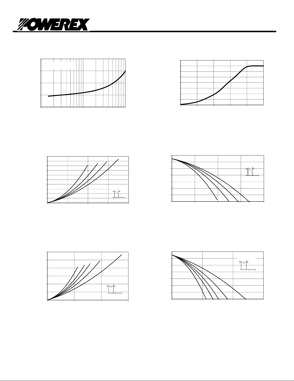
Maximum On-State Power Dissipation
Sinusoidal Waveform
90°
60°
Iavg (A)
atts)
Pavg (
10000
9000
8000
7000
6000
5000
4000
3000
2000
1000
0
0 1000 2000 3000 4000
120°
CONDUCTION ANGLE
0° 180° 360°
180°
MAXIMUM TRA N SIENT THERMAL
IMPEDANCE
8.E-03
7.E-03
6.E-03
5.E-03
4.E-03
3.E-03
2.E-03
1.E-03
0.E+00
0.001 0.01 0.1 1 10
Thermal Impedance (°C/Watt)
Maximum Allowable Case Temperature
Sinusoidal Waveform
°C)
Tc (
130
120
110
100
90
80
70
60
0 1000 2000 3000 4000
Time (sec)
60°
Iavg (A)
90°
CONDUCTION ANGLE
120°
0° 180° 360°
180°
Pavg (Watts)
Maximum On-State Power Dissipation
12000
10000
8000
6000
4000
2000
0
0 2000 4000 6000
Square Waveform
120°
90°
60°
Iavg (A)
180°
CONDUCTION ANGLE
360°
0° 180° 360°
Page 4
Maximum Allowable Case Temperature
130
120
110
100
90
Tc (°C)
80
70
60
0 2000 4000 6000
Square Waveform
60°
90°
120°
180°
Iavg (A)
CONDUCTION ANGLE
0° 180° 360°
360°
 Loading...