

Page 1

6121 Baker Road,
Suite 108
Minnetonka, MN 55345
www.chtechnology.com
Phone (952) 933-6190
Fax (952) 933-6223
1-800-274-4284
Thank you for downloading this document from C&H Technology, Inc.
Please contact the C&H Technology team for the following questions -
Technical
Application
Assembly
Availability
Pricing
Phone – 1-800-274-4284
E-Mail – sales@chtechnology.com
www.chtechnology.com - SPECIALISTS IN POWER ELECTRONIC COMPONENTS AND ASSEMBLIES - www.chtechnology.com
Page 2
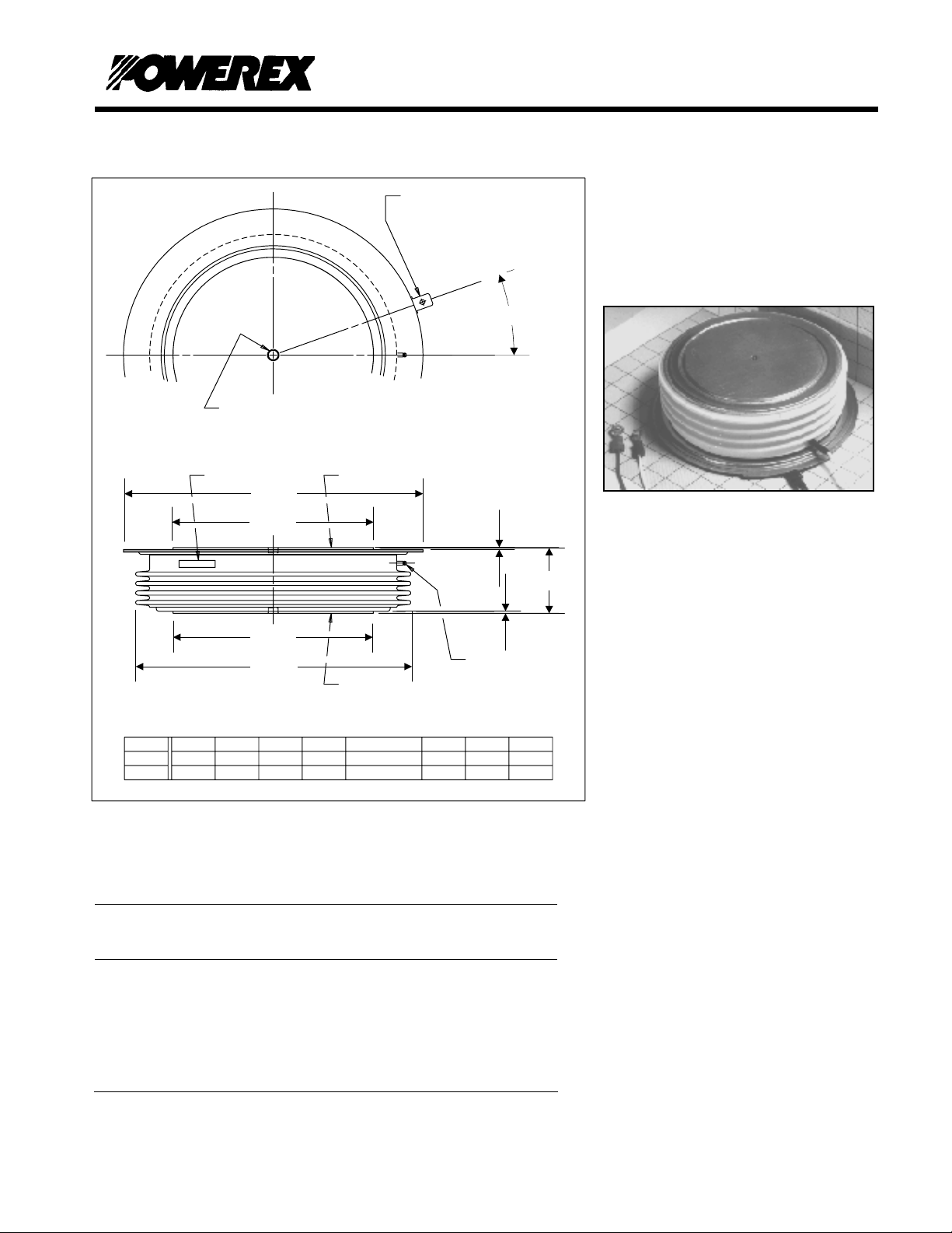
TBS7
3200A
Powerex, Inc., 173 Pavilion Ln, Youngwood, PA 15697 (412)925-7272 WWW.PWRX.COM
Phase Control Thyristor
3200 Amperes/Up to 1600 Volts
]
CATHODE POTENTIAL TERMINAL
FOR .187 INCH / 4.75 MM NOM.
PUSH-ON TYPE TERMINAL
Description:
Powerex Silicon Controlled Rectifiers (SCR) are
designed for phase control applications. These
are all-diffused, hermetic Pow-R-Disc devices
employing the field-proven amplifying gate.
H
]
F DIA. TYP.
G DEEP TYP.
MARKING CATHODE
B DIA.
A DIA.
A DIA.
C DIA.
ANODE
CASE NUMBER
NOMINAL DIMENSIONS
INCHES
MM
TBS
ABCD E FGHSYM.
2.88
73.2
4.36
110.7
ALL DIMENSIONS ARE REFERENCE
STRIKE DISTANCE = .62 INCH / 15.7 MM MIN.
CREEPAGE DISTANCE = 1.00 INCH / 25.4 MM MIN.
3.95
100.3
.030
0.76
1.010/1.080
25.65/27.43
.140
3.56
Ordering Information
Select the complete 12 digit device part number from the table below.
Type Voltage
V
DRM
V
RRM
TBS7 12
Current
I
T(av)
32 0 3 DH
Turn-Off
tq
Gate
Current
I
GT
14
16
1200 V
1400 V
1600 V
3200 A
350 µs
typical
200 mA 12"
D
D
GATE TERMINAL
FOR .058 INCH /
1.47 MM DIA. NOM.
PIN RECEPTACLE
O
20
.080
2.03
O
20
Lead
Code
Features:
E
Low On-State Voltage
High di/dt Capability
High dv/dt Capability
Excellent Surge and I
2
t Ratings
Applications:
Power Supplies
Battery Chargers
Motor Controllers
TBS716P13.DOC.12/10/97
Page 3

TBS7
3200A
Powerex, Inc., 173 Pavilion Ln, Youngwood, PA 15697 (412)925-7272 WWW.PWRX.COM
Phase Control Thyristor
3200 Amperes/Up to 1600 Volts
Absolute Maximum Ratings
Characteristics
Non-repetitive Transient Peak Reverse Voltage V
RMS On-State Current I
Average Current 180° Sine Wave, TC=76°C
Peak One Cycle Surge On-State Current (Non-Repetitive)
I
I
Symbol
V
RSM
5025 A
T(RMS)
3200 A
T(AV)
44,000 A
TSM
+100V V
RRM
Units
60Hz
Peak One Cycle Surge On-State Current (Non-Repetitive)
I
40500 A
TSM
50Hz
Critical Rate-of-Rise of On-State Current (Non-Repetitive) di/dt 300
Critical Rate-of-Rise of On-State Current (Repetitive) di/dt 100
I2t for Fusing for One Cycle, 60 Hz I2t 8.07x10⁶ A
A/µs
A/µs
2
s
Peak Gate Power Dissipation PGM 250 W
Average Gate Power Dissipation P
35 W
G(av)
Operating Temperature TJ
Storage Temperature T
STG
-40 to 125°C °C
-40 to 150°C °C
Mounting Force 6000 to 10000
26.6 to 44.4
TBS716P13.DOC.1/19/2006
Information presented is based upon manufacturers testing and projected
capabilities. This information is subject to change without notice. The
manufacturer makes no claim as to suitability for use, reliability, capability or
future availability of this product.
lb.
kN
Page 4

TBS7
3200A
Powerex, Inc., 173 Pavilion Ln, Youngwood, PA 15697 (412)925-7272 WWW.PWRX.COM
Phase Control Thyristor
3200 Amperes/Up to 1600 Volts
Electrical Characteristics, TJ=25°C unless otherwise specified
Characteristics Symbol Test Conditions Min. Typ. Max. Units
Repetitive Peak Reverse Leakage
Current
Repetitive Peak Forward Leakage
Current
Peak On-State Voltage VTM
I
I
RRM
DRM
T
=125°C, VR=V
J
T
=125°C, VD=V
J
T
=25°C, ITM=3000A
J
RRM
DRM
150 mA
150 mA
1.25 V
Duty Cycle < 0.01%
Threshold Voltage, Low-level V
Slope Resistance, Low-level rT1 0.0889
Threshold Voltage, High-level
Slope Resistance, High-level rT2 0.0735
ABCD V
Modeling Coefficients
TM
Typical Delay Time td I
V
(TO)1
(TO)2
A
B
C
D
T
=125°C, for 500A≤ITM<10,000A
J
0.776 V
mΩ
T
=125°C, for ITM<10,0000A
J
1.032 V
mΩ
TJ=125°C, for 500A≤ITM<60,000A
0.7393
-0.01883
0.05747
=1000A, VD=0.5V
TM
3
DRM
0.005836
V
-
mΩ
−
µs
Maximum Turn-Off Time tq
Minimum Critical dv/dt Expodential to V
DRM
dv/dt
Gate Trigger Current IGT
Gate Trigger Voltage VGT
Non-Triggering Gate Voltage V
Peak Forward Gate Current I
Peak Reverse Gate Voltage V
T
=125°C, IT=1000A, diR/dt=25A/µs
J
dv/dt=20V/µs linear to 80% V
T
=125°C
J
T
=25°C, VD=12V
J
T
=25°C, VD=12V
J
GDM
4A
GTM
10 V
GRM
T
=125°C, VD=V
J
DRM
DRM
350
300
µs
V/µs
200 mA
4.0 V
0.5 V
Thermal Characteristics
Characteristics Symbol Min. Typ. Max. Units
Maximum Thermal Resistance, Double
Sided Cooling
Junction to Case
Case to Sink
R
ΘJC
R
ΘCS
.010
.002
TBS716P13.DOC.12/10/97
°C/W
°C/W
 Loading...